STA575
100+100W STEREO
■
■
POWER AMPLIFIER
MONOCHIP BRIDGE STEREO AMPLIFIER
ON BASH ® ARCHITECTURE
80+80W OUTPUT POWER @ RL = 4/8 Ω,
THD = 0.5%
100+100W OUTPUT POWER @ RL = 4/8 Ω,
THD = 10%
HIGH DYNAMIC PREAMPLIFIER INPUT
STAGES
EXTERNAL PROGRAMMABLE FEEDBACK
TYPE COMPRESSORS
AC COUPLED INPUT TO CLASS AB BRIDGE
OUTPUT AMPLIFIER
PRECISION RECTIFIERS TO DRIVE THE
DIGITAL CONVERTER
ON-OFF SEQUENCE/ TIMER WITH MUTE
AND STANDBY
PROPORTIONAL OVER POWER OUTPUT
CURRENT TO LIMIT THE DIGITAL
CONVERTER
ABSOLUTE POWER BRIDGE OUTPUT
)
s
(
t
c
u
d
o
)
r
s
(
P
t
c
e
t
u
e
d
l
o
o
r
s
P
b
e
O
t
e
l
)
o
s
(
s
t
b
c
u
O
d
o
)
r
s
P
(
t
c
e
t
u
e
l
d
o
o
r
s
P
b
O
e
t
e
l
o
s
b
O
■
■
■
■
■
■
■
■
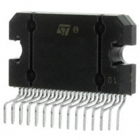
FLEXIWATT27
■
■
■
■
■
TRANSISTOR POWER PROTECTION
ABSOLUTE OUTPUT CURRENT LIMIT
INTEGRATED THERMAL PROTECTION
POWER SUPPLY OVER VOLTAGE
PROTECTION
FLEXIWATT POWER PACKAGE WITH 27 PIN
BASH® LICENCE REQUIRED
DESCRIPTION
The STA575 is a fully integrated power module designed to implement a BASH® amplifier when used
in conjunction with STABP01 digital processor.
BLOCK DIAGRAM
+VS
GND
-VS
OUT_ PRE1
TRK_1
PWR_INP1
ABSOLUTE
VALUE
BLOCK
+
-
CD+1
+2
∆G
IN_PRE1
OUT1+
-1
OUT1-
COMPRESSOR
OUTPUT BRIDGE
CD-1
V/l
ATT_REL1
CD+
PEAK/2
DETECTOR
S1
Ict
VOLTAGE
PROTECTION
Ict
THERMAL
PROTECTION
SOA
DETECTOR
PROT.
TURNON/OFF
SEQUENCE
STBY/MUTE
TRK_OUT
THRESH
PEAK/2
DETECTOR
S1
ATT_REL2
V/l
CD+2
+2
COMPRESSOR
-1
-
ABSOLUTE
VALUE
BLOCK
+
OUT_ PRE2
July 2003
OUT2+
∆G
IN_PRE2
TRK_2
OUT2-
OUTPUT BRIDGE
PWR_INP2
CD-2
D01AU1263
1/20
�STA575
DESCRIPTION (continued)
Notice that normally only one Digital Converter is needed to supply a stereo or multi-channel amplifier system,
therefore most of the functions implemented in the circuit have summing outputs
The signal circuits are biased by fixed negative and positive voltages referred to Ground. Instead the final stages of the output amplifiers are supplied by two external voltages that are following the audio signal . In this way
the headroom for the output transistors is kept at minimum level to obtain a high efficiency power amplifier.
The Compressor circuits, one for each channel, performs a particular transfer behavior to avoid the dynamic
restriction that an adaptive system like this requires. To have a high flexibility the attack / release time and the
threshold levels are externally programmable. The tracking signal for the external digital converter is generated
from the Absolute Value block that rectifies the audio signal present at the compressor output. The outputs of
these blocks are decoupled by a diode to permit an easy sum of this signal for the multichannel application. The
output power bridges have a dedicated input pin to perform an AC decoupling to cancel the compressor output
DC offset. The gain of the stage is equal to 4 (+12dB). A sophisticated circuit performs the output transistor power detector that , with the digital converter, reduces the power supply voltage . Moreover, a maximum current
output limiting and the over temperature sensor have been added to protect the circuit itself. The external voltage applied to the STBY/MUTE pin forces the two amplifiers in the proper condition to guarantee a silent turnon and turn-off.
)
s
(
t
c
u
d
o
)
r
s
(
P
t
c
e
t
u
e
d
l
o
o
r
s
P
b
e
O
t
e
l
)
o
s
(
s
t
b
c
u
O
d
o
)
r
s
P
(
t
c
e
t
u
e
l
d
o
o
r
s
P
b
O
e
t
e
l
o
s
b
O
ABSOLUTE MAXIMUM RATINGS
Symbol
Parameter
Value
Unit
+Vs
Positive supply voltage referred to pin 13 (GND)
30
V
-Vs
Negative supply voltage referred to pin 13 (GND)
-24
V
VCD+
Positive supply voltage tracking rail referred to pin 13 (GND)
22
V
VCD+
Positive supply voltage operated to Vs+(1)
0.3
V
VCD-
Negative supply voltage referred to -Vs (1)
-0.3
V
VCD-
Negative supply voltage tracking rail referred to pin 13 (GND)
-22
V
VAtt_Rel1
VAtt_Rel2
Pin 3, 25 Negative & Positive maximum voltage referred to GND
(pin 13)
-0.5 to +20
V
VPwr_Imp1
VPwr_Imp2
VTrk_1
VTrk_2
Pin 7, 21, 18, 10 Negative & Positive maximum voltage referred to
GND (pin 13)
-20 to +20
V
VIn_pre1
VIn_pre2
Pin 8, 20 Negative & Positive maximum voltage referred to GND
(pin 13)
-0.5 to +0.5
V
Vthreshold
Pin 17 Negative & Positive maximum voltage referred to GND (pin
13)
-7 to +0.5
V
Pin 11 maximum input current (Internal voltage clamp at 5V)
500
µA
Pin 11 negative maximum voltage referred to GND (pin 13)
-0.5
V
Output current
7.7
A
Istb-max
Vstbymute
Iout
Note 1: VCD- must not be more negative than -Vs and VCD+ must not be more positive than +VS
Note 2: All pins withstand ±2KV ESD but not pin 11
2/20
�STA575
THERMAL DATA
Symbol
Tj
Parameter
Value
Unit
150
°C
1
°C/W
Value
Unit
+20 to +28
V
Max Junction temperature
Rth j_case Thermal Resistance Junction to case .............................. ..max
OPERATING RANGE
Symbol
+Vs
Parameter
Positive supply voltage
)
s
(
t
c
u
d
o
)
r
s
(
P
t
c
e
t
u
e
d
l
o
o
r
s
P
b
e
O
t
e
l
)
o
s
(
s
t
b
c
u
O
d
o
)
r
s
P
(
t
c
e
t
u
e
l
d
o
o
r
s
P
b
O
e
t
e
l
o
s
b
O
-Vs
Negative supply voltage
-10 to -23
V
5V ≤ (Vs+ - VCD+) ≤ 10V
V
∆Vs+
Delta positive supply voltage
VCD+
Positive supply voltage tracking rail
+3 to 20.7
V
VCD-
Negative supply voltage tracking rail
-20.7 to -3
V
Current at pin In_Pre1, In_Pre2, related to compressor behaviour
-1 to +1
mA peak
Voltage at pin Threshold
-5 to 0
V
Ambient Temperature Range
0 to 70
°C
200
µA
Iin_Max
Vtrheshold
Tamb
Isb_max
Pin 11 maximum input current (Internal voltage clmp at 5V)
PIN CONNECTION
CD-2
OUT2+
ATT_REL2
CD+2
OUT2-
IN_PRE2
PWR_INP2
TRK_2
OUT_PRE2
TRK_OUT
THRESHOLD
+VS
CD+
GND
PROTECTION
TRK_1
STBY/MUTE
IN_PRE1
OUT_PRE1
CD+1
PWR_INP1
OUT1-
OUT1+
ATT-REL1
-VS
CD-1
-Vs
27
1
D01AU1251
Note: Slug connected to pins n. 1 and 27
3/20
�STA575
PIN FUNCTION
N°
Name
Description
1
-Vs
2
CD-1
3
Att_Rel1
4
Out1+
Channel 1 speaker positive output
5
Out1-
Channel 1 speaker negative output
6
CD+1
Channel 1 positive power supply
7
Pwr_Inp1
8
In_pre1
9
Out_pre1
10
Trk_1
11
Stby/mute
Standby/mute input voltage control
12
Protection
Protection signal for STABP01 digital processor
13
Gnd
Analog Ground
14
+Vs
Positive Bias Supply
15
CD+
Time varying tracking rail positive power supply
16
Trk_out
Reference output for STABP01 digital processor
17
Threshold
18
Trk_2
19
Out_pre2
20
In_pre2
21
Pwr_Inp2
22
CD+2
Channel 2 positive power supply
23
Out2-
Channel 2 speaker negative output
24
Out2+
Channel 2 speaker positive output
25
Att_Rel2
26
CD-2
27
-Vs
Negative Bias Supply
Channel 1 Time varying tracking rail negative power supply
Attack release rate for channel 1
)
s
(
t
c
u
d
o
)
r
s
(
P
t
c
e
t
u
e
d
l
o
o
r
s
P
b
e
O
t
e
l
)
o
s
(
s
t
b
c
u
O
d
o
)
r
s
P
(
t
c
e
t
u
e
l
d
o
o
r
s
P
b
O
e
t
e
l
o
s
b
O
4/20
Input to channel 1 power stage
Pre-amp input for channel 1 (virtual ground)
Output channel 1 pre-amp
Absolute value block input for channel 1
Compressor threshold input
Absolute value block input for channel 2
Output channel 2 pre-amp
Pre-amp input for channel 2 (virtual ground)
Input to channel 2 power stage
Attack release rate for channel 2
Channel 2 Time varying tracking rail negative power supply
Negative Bias Supply
�STA575
ELECTRICAL CHARACTERISTCS (Test Condition: Vs+ = 28V, Vs- = -23V, V CD+ = 20V, VCD- = -20V, RL =
8Ω, external components at the nominal value f = 1KHz, Tamb = 25°C unless otherwise specified
Symbol
Parameter
Test Condition
Min.
Typ.
Max.
Unit
9
11
13
Vpeak
0.8
mA
0.65
12
V
V
V
-1
V
PREAMPLIFIER AND COMPRESSOR
Vout clamp Maximum Voltage at Out_pre pin
Iin
Audio input current
Vcontrol
Voltage at Attack_Release pin
Attenuation = 0dB
Attenuation = 6dB
Attenuation = 26dB
0.35
6
0
0.5
9
Th
Input voltage range for the
compression
Zth
Input impedance of Threshold pin
Voffset
Output Offset at Out_pre pin with:
VCRT= 0V; Attenuation = 0dB
VCRT= 0.5V; Attenuation = 6dB
VCRT= 9V; Attenuation = 26dB
THD
Distortion at Out_pre:
VCRT= 0V; Attenuation = 0dB
VCRT= 0.5V; Attenuation = 6dB
VCRT= 9V; Attenuation = 26dB
0.01
EN
Noise at Out_pre pin :
VCRT= 0V; Attenuation = 0dB
VCRT= 0.5V; Attenuation = 6dB
VCRT= 9V; Attenuation = 26dB
10(2)
50
60
Ict
Attack time current at pin
Attack_release
VComp_
-5
)
s
(
t
c
u
d
o
)
r
s
(
P
t
c
e
t
u
e
d
l
o
o
r
s
P
b
e
O
t
e
l
)
o
s
(
s
t
b
c
u
O
d
o
)
r
s
P
(
t
c
e
t
u
e
l
d
o
o
r
s
P
b
O
e
t
e
l
o
s
b
O
100
KΩ
-15
-250
-1000
15
250
450
mV
mV
mV
0.1
0.5
2
%
%
%
µV
µV
µV
0.5
1.5
3
mA
Tracking reference voltage gain
13
14
15
V
Vtrk_out
Tracking ref. output voltage
0
20
Itrk_out
Current capability
5
6
Ztrk_in
Input impedance (TRK1/2)
1. This value is due to the thermal noise of the external resistors Rr and Ri.
TRACKING PARAMETERS
Gtrk
V
7
1
mA
MΩ
OUTPUT BRIDGE
Gout
Half Output bridge gain
5.5
6
6.5
dB
Gch
Output bridge differential gain
11
12
13
dB
∆Gch
Output bridges gain mismatch
-0.5
0.5
dB
Pout
Continuous Output Power
THD
Total harmonic distortion of the
output bridge
THD = 0.5%
THD = 10%
75
95
80
100
W
W
THD = 10%; RL= 4Ω; VCD+ = 16V;
VCD- = -16V; VS+ = 22V; VS- = -22V
90
100
W
Po = 5W
0.01
f = 20Hz to 20KHz; Po = 50W
VOff
Output bridge D.C. offset
-70
0.1
%
0.2
%
70
mV
5/20
�STA575
ELECTRICAL CHARACTERISTCS (continued)
Symbol
EN
Parameter
Noise at Output bridge pins
Test Condition
Min.
f = 20Hz to 20KHz; Rg = 50Ω
Typ.
Max.
Unit
µV
12
Zbr_in
Input impedance
Rdson
Output power Rdson
OLG
Open Loop Voltage Gain
100
dB
GB
Unity Gain Bandwidth
1.4
MHz
SR
Slew Rate
8
V/µs
100
IO = 1A
140
180
KΩ
200
400
mΩ
)
s
(
t
c
u
d
o
)
r
s
(
P
t
c
e
t
u
e
d
l
o
o
r
s
P
b
e
O
t
e
l
)
o
s
(
s
t
b
c
u
O
d
o
)
r
s
P
(
t
c
e
t
u
e
l
d
o
o
r
s
P
b
O
e
t
e
l
o
s
b
O
PROTECTION
Vstby
Stby voltage range
0
0.8
V
Vmute
Mute voltage range
1.6
2.5
V
Vplay
Play voltage range
4
5
V
Th1
First Over temperature threshold
130
°C
Th2
Second Over temperature
threshold
150
°C
Unbal.
Ground
Upper Unbalancing ground
threshold
Referred to (CD+ - CD-)/2
5
V
Unbal.
Ground
Lower Unbalancing ground
threshold
Referred to (CD+ - CD-)/2
-5
V
Under voltage threshold
|Vs+| + |Vs-|
18
20
22
V
Pd_reg.
Power dissipation threshold for
system regulation
Iprot = 50µA; @ Vds = 10V
26
32
39
W
Pd_max
Switch off power dissipation
threshold
@ Vds = 10V
60
W
Iprot
Protection current slope
for Pd > Pdreg
400
µA/W
Ilct
Limiting Current threshold
UVth
I+Vs
I-Vs
Positive supply current
Negative supply current
6.3
7
7.5
A
Stby (Vstby/mute pin = 0V)
Mute (Vstby/mute pin = 2.5V)
Play (Vstby/mute pin = 5V no signal)
20
20
5
35
35
7
50
50
mA
mA
mA
Stby (Vstby/mute pin = 0V)
Mute (Vstby/mute pin = 2.5V)
Play (Vstby/mute pin = 5V no signal)
20
20
5
35
35
7
50
50
mA
mA
mA
ICD+
Positive traking rail supply current
Stby (Vstby/mute pin = 0V)
Mute (Vstby/mute pin = 2.5V)
Play (Vstby/mute pin = 5V no signal)
50
60
60
100
110
110
200
180
180
µA
mA
mA
ICD-
Negative traking rail supply current Stby (Vstby/mute pin = 0V)
Mute (Vstby/mute pin = 2.5V)
Play (Vstby/mute pin = 5V no signal)
50
60
60
100
110
110
200
180
180
µA
mA
mA
6/20
�STA575
FUNCTIONAL DESCRIPTION
The circuit contains all the blocks to build a stereo amplifier. Each single channel is based on the Output Bridge
Power Amplifier, and its protection circuit. Moreover, the compression function and a signal rectifier are added
to complete the circuit.
The operation modes are driven by The Turn-on/off sequence block. In fact the IC can be set in three states by
the Stby/mute pin:
Standby ( Vpin < 0.8V), Mute (1.6V < Vpin < 2.5V), and Play (Vpin > 4V).
In the Standby mode all the circuits involved in the signal path are in off condition, instead
in Mute mode the circuits are biased but the Speakers Outputs are forced to ground potential.
These voltages can be get by the external RC network connected to Stby/Mute pin.
The same block is used to force quickly the I.C. In standby mode or in mute mode when the I.C. dangerous
condition has been detected. The RC network in these cases is used to delay the Normal operation restore.
)
s
(
t
c
u
d
o
)
r
s
(
P
t
c
e
t
u
e
d
l
o
o
r
s
P
b
e
O
t
e
l
)
o
s
(
s
t
b
c
u
O
d
o
)
r
s
P
(
t
c
e
t
u
e
l
d
o
o
r
s
P
b
O
e
t
e
l
o
s
b
O
The protection of the I.C. are implemented by the Over Temperature, Unbalance Ground, Output Short circuit,
Under voltage, and output transistor Power sensing as shown in the following table:
Table 1. Protection Implementation
Fault Type
Condition
Protection strategy
Action time
Release time
Chip Over
temperature
Tj > 130 °C
Mute
Fast
Slow Related to
Turn_on sequence
Chip Over
temperature
Tj > 150 °C
Standby
Fast
Slow, Related to
Turn_on sequence
Unbalancing
Ground
|Vgnd| > ((CD+) (CD-))/2 + 5V
Standby
Fast
Slow, Related to
Turn_on sequence
Short circuit
Iout > 7A
Standby
Fast
Slow, related to
Turn_on sequence
Under Voltage
|Vs+| + |Vs-|< 20V
Standby
Fast
Slow, related to
Turn_on sequence
Extra power
dissipation
at output transistor
Pd tr. > 32W
Reducing DIGITAL
CONVERTER output
voltage.
Related to the
DIGITAL
CONVERTER
Related to the
DIGITAL
CONVERTER
Maximum power
dissipation
at output transistor
Pd tr. > 60W
Standby
Fast
Slow, related to
Turn_on sequence
See the POWER PROTECTION paragraph for the details
Compression
An other important function implemented, to avoid high power dissipation and clipping distortion, is the Compression of the signal input. In fact the preamplifier stage performs a voltage gain equal to 5, fixed by Ri and Rr
external resistor, but in case of high input signal or low power supply voltage, its gain could be reduced of 26dB.
This function is obtained with a feedback type compressor that , in practice, reduces the impedance of the external feedback network. The behavior of compression it's internally fixed but depends from the Audio input voltage signal level, and from the Threshold voltage applied to the Threshold pin. The attack and release time are
programmable by the external RC network connected to the Att_Rel pins.
The constraints of the circuit in the typical application are the following:
Vthreshold range
= -5 to 0
Vin peak max
= 8V
Vout peak max
= 10V
7/20
�STA575
Gain without compression (G)
=5
Max Attenuation ratio
= 26 dB
The following graph gives the representation of the Compressor activation status related to the Vthreshold and
the input voltage. The delimitation line between the two fields, compression or not, is expressed by the formula :
2 ⋅ ( Vth resho ld + 200 mV )
-------------------------------------------------------------------------G
Where G is the preamplifier gain without compression.
In the compression region the gain of the preamplifier will be reduced
(G = 2·Vthreshold/Vin) to maintain at steady state the output voltage equal 2*|Vthreshold| .
)
s
(
t
c
u
d
o
)
r
s
(
P
t
c
e
t
u
e
d
l
o
o
r
s
P
b
e
O
t
e
l
)
o
s
(
s
t
b
c
u
O
d
o
)
r
s
P
(
t
c
e
t
u
e
l
d
o
o
r
s
P
b
O
e
t
e
l
o
s
b
O
Instead in the other region the compressor will be off (G = 5).
The delimitation line between the two fields can be related to the output voltage of the preamplifier: in this case
the formula is :
V out = 2 ⋅ ( Vthre sho ld + 200mV )
Figure 1. Compressor activation field
VIN PEAK
8
6
COMPRESSION
G ---------------------I in_max
8/20
�STA575
Figure 2. Compressor attenuation vs. input amplitude
Attenuation(dB)
0
-6
|Vth
-12
=5|
|Vth
)
s
(
t
c
u
d
o
)
r
s
(
P
t
c
e
t
u
e
d
l
o
o
r
s
P
b
e
O
t
e
l
)
o
s
(
s
t
b
c
u
O
d
o
)
r
s
P
(
t
c
e
t
u
e
l
d
o
o
r
s
P
b
O
e
t
e
l
o
s
b
O
-18
|Vt
=2.
5|
h=
1|
-24
D01AU1265
1
2
3
4
5
6
7
8
|Vinpk|
ABSOLUTE VALUE BLOCK
The absolute value block rectifies the signal after the compression to extract the control voltage for the external
digital converter. The output voltage swing is internally limited, the gain is internally fixed to 14.
The input impedance of the rectifier is very high , to allow the appropriate filtering of the audio signal before the
rectification (between Out_pre and Trk pins).
OUTPUT BRIDGE
The Output bridge amplifier makes the single-ended to Differential conversion of the Audio signal using two
power amplifiers, one in non-inverting configuration with gain equal to 2 and the other in inverting configuration
with unity gain. To guarantee the high input impedance at the input pins, Pwr_Inp1 and Pwr_Inp2, the second
amplifier stages are driven by the output of the first stages respectively.
POWER PROTECTION
To protect the output transistors of the power bridge a power detector is implemented (fig 3).
The current flowing in the power bridge and trough the series resistor Rsense is measured reading the voltage
drop between CD+1 and CD+. In the same time the voltage drop on the relevant power (Vds) is internally measured. These two voltages are converted in current and multiplied: the resulting current , Ipd, is proportional to
the instantaneous dissipated power on the relevant output transistor. The current Ipd is compared with the reference current Ipda, if bigger (dissipated power > 32W) a current, Iprot, is supplied to the Protection pin. The
aim of the current Iprot is to reduce the reference voltage for the digital converter supplying the power stage of
the chip, and than to reduce the dissipated power. The response time of the system must be less than 200µSec
to have an effective protection. As further protection, when Ipd reaches an higher threshold (when the dissipated
value is higher then 60W) the chip is shut down, forcing low the Stby/Mute pin, and the turn on sequence is
restarted.
9/20
�STA575
Figure 3. Power Protection Block Diagram
RSENSE
CD+
CD+1
ILOAD
V/I
OC1
ILIM
TO TURN-ON/OFF
SEQUENCE
CURRENT COMP
)
s
(
t
c
u
d
o
)
r
s
(
P
t
c
e
t
u
e
d
l
o
o
r
s
P
b
e
O
t
e
l
)
o
s
(
s
t
b
c
u
O
d
o
)
r
s
P
(
t
c
e
t
u
e
l
d
o
o
r
s
P
b
O
e
t
e
l
o
s
b
O
MULTIPLIER
X
PDP1
IPD
V/I
IPDP
I_PD
CURRENT COMP
IPD
OPA
TO TURN-ON/OFF
SEQUENCE
IPROT
TO PROT PAD
OPA
IPDA
OUT1+
CD-
D01AU1266
OUT1-
In fig. 3 there is the power protection strategy pictures. Under the curve of the 32W power, the chip is in normal
operation, over 60W the chip is forced in Standby. This last status would be reached if the digital converter does
not respond quikly enough reducing the stress to less than 60W.
The fig.4 gives the protection current, Iprot, behavior. The current sourced by the pin Prot follows the formula:
–4
( Pd – Pd_av _th ) ⋅ 5 ⋅ 10
Iprot ≡ -----------------------------------------------------------------1.25V
for Pd < Pd_av_th the Iprot = 0
Independently of the output voltage, the chip is also shut down in the folowing conditions:
When the currentthrough the sensing resistor, R sense, reaches 7A (Voltage drop (CD+) - (CD+1) = 700mV).
When the average junction temperature of the chip reaches 150°C.
When the ground potential differ from more than 5V from the half of the power supply voltage, ((CD+)-(CD-))/2
When the sum of the supply voltage |Vs+| + |Vs-|