STA8088FG
Fully Integrated GPS/Galileo/Glonass/QZSS Receiver
with embedded RF and in-package Flash
Data brief preliminary data
Features
■
STMicroelectronics® 3rd generation positioning
receiver with 32 Tracking channels and 2 fast
acquisition channels compatible with GPS,
Galileo and Glonass systems
■
Embedded RF Front-End with separate
GPS/Galieo/QZSS and Glonass IF outputs
■
Embedded low noise amplifier
■
-162 dBm indoor sensitivity (tracking mode)
■
Fast TTFF < 1 s in Hot start and 35 s in Cold
Start
■
High performance ARM946 MCU (up to
208 MHz)
■
256 Kbyte embedded SRAM
■
In-Package SQI Flash Memory (16 Mbits)
■
Real Time Clock (RTC) circuit
■
32-bit Watch-dog timer
■
3 UARTs
■
1 I2C master/slave interface
■
1 Synchronous Serial Port (SSP, Motorola-SPI
supported) or 1 External SQI Flash interface
■
USB2.0 dual-role full speed (12 MHz) with
integrated physical layer transceiver
■
2 Controller Area Network (CAN)
■
2 channels ADC (10 bits)
■
3 Embedded 1.8 V voltage regulators
■
I/O level selectable 1.8 V or 3.3 V
■
Operating Condition:
– VDD12: 1.2 V ±10%
– VDD18/RF18: 1.8 V ±5%
– VLPVR 1.62 V to 3.6 V
– VddIO: 1.8 V ±5%; 3.3 V ±10%
September 2013
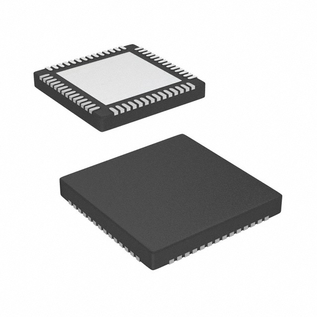
VFQFPN56
(7x7x0.85mm)
■
Package:
– VFQFPN56 (7 x 7 x 0.85 mm) 0.4 mm
pitch
■
Ambient temperature range: -40/+85°C
Description
STA8088FG is a single die standalone positioning
receiver IC working on multiple constellations
(GPS/Galileo/Glonass/QZSS).
The minimum BOM make STA8088FG the ideal
solution for low-cost and small footprint products
such handheld computers, cameras, data
loggers, and sports accessories.
The device is offered with a complete GNSS
firmware which performs all GNSS operations
including tracking, acquisition, navigation and
data output with no need of external memories
Doc ID 022731 Rev 3
This is preliminary information on a new product now in development or undergoing evaluation. Details are subject to
change without notice. For further information contact your local STMicroelectronics sales office.
1/17
www.st.com
1
�Contents
STA8088FG
Contents
1
Overview . . . . . . . . . . . . . . . . . . . . . . . . . . . . . . . . . . . . . . . . . . . . . . . . . . 5
2
Pin description . . . . . . . . . . . . . . . . . . . . . . . . . . . . . . . . . . . . . . . . . . . . . 6
3
2.1
Block diagram . . . . . . . . . . . . . . . . . . . . . . . . . . . . . . . . . . . . . . . . . . . . . . . 6
2.2
VFQFPN56 pin configuration
2.3
Power supply pins . . . . . . . . . . . . . . . . . . . . . . . . . . . . . . . . . . . . . . . . . . . 8
2.4
Main function pins . . . . . . . . . . . . . . . . . . . . . . . . . . . . . . . . . . . . . . . . . . . 9
2.5
Test/emulated dedicated pins . . . . . . . . . . . . . . . . . . . . . . . . . . . . . . . . . 10
2.6
RF front-end pins . . . . . . . . . . . . . . . . . . . . . . . . . . . . . . . . . . . . . . . . . . . 10
2.7
Port 0 pins . . . . . . . . . . . . . . . . . . . . . . . . . . . . . . . . . . . . . . . . . . . . . . . . 10
2.8
Port 1 pins . . . . . . . . . . . . . . . . . . . . . . . . . . . . . . . . . . . . . . . . . . . . . . . . 11
.................................. 7
Package and packing information . . . . . . . . . . . . . . . . . . . . . . . . . . . . . 13
3.1
ECOPACK® packages . . . . . . . . . . . . . . . . . . . . . . . . . . . . . . . . . . . . . . . 13
3.2
VFQFPN56 7 x 7 x 0.85 mm package information . . . . . . . . . . . . . . . . . . 13
4
Ordering information . . . . . . . . . . . . . . . . . . . . . . . . . . . . . . . . . . . . . . . 15
5
Revision history . . . . . . . . . . . . . . . . . . . . . . . . . . . . . . . . . . . . . . . . . . . 16
2/17
Doc ID 022731 Rev 3
�STA8088FG
List of tables
List of tables
Table 1.
Table 2.
Table 3.
Table 4.
Table 5.
Table 6.
Table 7.
Table 8.
Power supply pins. . . . . . . . . . . . . . . . . . . . . . . . . . . . . . . . . . . . . . . . . . . . . . . . . . . . . . . . . 8
Main function pins . . . . . . . . . . . . . . . . . . . . . . . . . . . . . . . . . . . . . . . . . . . . . . . . . . . . . . . . . 9
Test/emulated dedicated pins . . . . . . . . . . . . . . . . . . . . . . . . . . . . . . . . . . . . . . . . . . . . . . . 10
RF front-end pins . . . . . . . . . . . . . . . . . . . . . . . . . . . . . . . . . . . . . . . . . . . . . . . . . . . . . . . . 10
Port 0 pins. . . . . . . . . . . . . . . . . . . . . . . . . . . . . . . . . . . . . . . . . . . . . . . . . . . . . . . . . . . . . . 11
Port 1 pins . . . . . . . . . . . . . . . . . . . . . . . . . . . . . . . . . . . . . . . . . . . . . . . . . . . . . . . . . . . . . 11
VFQFPN56 package dimensions . . . . . . . . . . . . . . . . . . . . . . . . . . . . . . . . . . . . . . . . . . . . 13
Document revision history . . . . . . . . . . . . . . . . . . . . . . . . . . . . . . . . . . . . . . . . . . . . . . . . . 16
Doc ID 022731 Rev 3
3/17
�List of figures
STA8088FG
List of figures
Figure 1.
Figure 2.
Figure 3.
Figure 4.
Figure 5.
4/17
STA8088FG system block diagram . . . . . . . . . . . . . . . . . . . . . . . . . . . . . . . . . . . . . . . . . . . 6
VFQFPN56 connection diagram - with CAN (bottom view) . . . . . . . . . . . . . . . . . . . . . . . . . 7
VFQFPN56 connection diagram - no CAN (bottom view). . . . . . . . . . . . . . . . . . . . . . . . . . . 8
VFQFPN56 7 x 7 x 0.85 mm package dimension. . . . . . . . . . . . . . . . . . . . . . . . . . . . . . . . 14
Ordering information scheme . . . . . . . . . . . . . . . . . . . . . . . . . . . . . . . . . . . . . . . . . . . . . . . 15
Doc ID 022731 Rev 3
�STA8088FG
1
Overview
Overview
STA8088FG is a highly integrated System-On-Chip device designed for positioning systems
applications.
The low power consumption and minimum BOM make STA8088FG the ideal solution for
low-cost and battery-operated portable products such handheld, computers, cameras, data
loggers and sports accessories, as well as automotive application.
It combines a high performance ARM946 microprocessor with embedded enhanced
peripherals and I/O capabilities with ST next generation triple-constellation positioning
engine. The RF front-end and base band processor are able to support GPS/Galileo and
Glonass navigation systems. The device is offered with a complete firmware which performs
all positioning operations including tracking, acquisition, navigation and data output with no
need of external memories.
It also provides clock generation via PLL, backup logic with real time clock and it supports
USB2.0 standard at full speed, (12 Mbps) with on-chip PHY.
STA8088FG is software compatible with the ARM processor family. The device is power
supplied with 1.8V and uses three on-chip voltage regulators to internally supply the RF
front-end, core logic and the backup logic. In order to reduce the power consumption the
chip can be directly powered with 1.2 V bypassing the embedded voltage regulators which
will be put in power down mode.
I/O lines are compatible with 1.8 V and 3.3 V.
The chip, using STMicroelectronics CMOSRF Technology, is housed in a VFQFPN-56
(7 x 7 x 0.85 mm) package with stacked 16 Mbit Flash memory.
Doc ID 022731 Rev 3
5/17
�Pin description
STA8088FG
2
Pin description
2.1
Block diagram
Figure 1.
STA8088FG system block diagram
CLOCK_GEN
G3RF IP
G3 Base Band
32 Trk
Channels
APB
Bridge
2 Fast Acq
Channel
GALGPS IF
ADC
GALGPS
LNA
Section
Glonass IF
ADC
GLONASS
RF
Section
OSCI
26MHz
CKX2
1.8V �1.2V
DCREG
Mux
Acq
RAMs
PLL
PG_650x
SPI IF
FRC_DPLL
AHB
RIOSC47
SQI
IF
USB
IF
IOs
CAN0
ROM
16KB
APB
Bridge2
UART
Rx-Tx
CAN1
UART1
Rx - Tx
UART2
Rx - Tx
SSP
I2C
JTAG
APB
WD
EFT
GPIO
MTU
ADC
REGMAP
THSENS
VIC
BK_domain
Test controller
SARADC
I/D SWITCHABLE TCM
8x16KB
64KHIGH SPEED D – TCM 8
I-Cache
16KB
ARM 946
D-Cache
8KB
HIGH SPEED I - TCM
64KB
RAM 8KB
APB
Bridge1
SYS CTRL
AD10SA1M_18
PWR, RST & CLK
CTRL
DC_LN_1V8TO1V2
APB
HPREG
OSCI32
OSCI32_LJ_1V8
ISO
CELL
RTC
LPREG
DCREG
OSCI32
BKREG
GAPGCFT00542
6/17
Doc ID 022731 Rev 3
�STA8088FG
Pin description
'0)/���0����
6$$��?-62�
53"?$0�5!24�?48
53"?$-�5!24�?2 8
4$/
#!.�48
6$$?)/2�
4$)
#!.�28
)�#?3$�#!.�48 �0���
4#+
VFQFPN56 connection diagram - with CAN (bottom view)
6$$?)/2�
Figure 2.
6$$?)/2�
VFQFPN56 pin configuration
330?$/�0���
2.2
��
��
��
��
��
��
��
��
��
��
��
��
��
��
330?$)�0���
��
�
)�#?3#,+�#!.�28 �0���
330?#,+�0���
��
�
4-3
330?#3.�0���
��
�
4234N
5!24�?48�"//4?� �0���
��
�
6$$��?-62�
5!24�?28 �0���
��
�
40?)&?0
5!24�?48�"//4?� �0���
��
�
40?)&?.
5!24�?28�0���
��
�
62&��?2&!$#
'0)/�0���
��
�
62&��?,.!
6$$?)/2�
��
�
,.!?).
!$#?).�
��
��
'.$?,.!
!$#?).�
��
��
,.!?/54
6$$��?-62�
��
��
62&��/54?2&62
6$$��?-62�
��
��
62&��?2&62
6$$?,062
��
��
62&��?2&!
��
��
��
��
��
��
��
��
��
��
��
��
��
��
24#?84/
24#?84)
7!+%50
234N
34$"9N
34$"9/54
6$$��?-62�
6$$��?,062
84!,?/54
84!,?).
62&��?2&6#/
62&��?)&
62&��?-)8
2&!?).
%0
Doc ID 022731 Rev 3
("1($'5�����
7/17
�Pin description
6$$?)/2�
'0)/���0����
6$$��?-62�
53"?$0�5!24�?48
53"?$-�5!24�?2 8
4$/
.�#�
6$$?)/2�
4$)
.�#�
)�#?3$ �0���
4#+
��
��
��
��
��
��
��
��
��
��
��
��
��
��
6$$?)/2�
VFQFPN56 connection diagram - no CAN (bottom view)
330?$/�0���
Figure 3.
STA8088FG
330?$)�0���
��
�
)�#?3#,+ �0���
330?#,+�0���
��
�
4-3
330?#3.�0���
��
�
4234N
5!24�?48�"//4?��0���
��
�
6$$��?-62�
5!24�?28 �0���
��
�
40?)&?0
5!24�?48�"//4?� �0���
��
�
40?)&?.
5!24�?28 �0���
��
�
62&��?2&!$#
'0)/�0���
��
�
62&��?,.!
6$$?)/2�
��
�
,.!?).
!$#?).�
��
��
'.$?,.!
!$#?).�
��
��
,.!?/54
6$$��?-62�
��
��
62&��/54?2&62
6$$��?-62�
��
��
62&��?2&62
6$$?,062
��
��
62&��?2&!
��
��
��
��
��
��
��
��
��
��
��
��
��
��
24#?84/
24#?84)
7!+%50
234N
34$"9N
34$"9/54
6$$��?-62�
6$$��?,062
84!,?/54
84!,?).
62&��?2&6#/
62&��?)&
62&��?-)8
2&!?).
%0
2.3
Power supply pins
Table 1.
Power supply pins
("1($'5�����
Symbol
I/O
VDD18_MVR[1,2]
Pwr
Digital supply voltage for main voltage regulator (1.8 V)
VDD12_MVR[1,2,3]
Pwr
Digital supply voltage for core circuitry (1.2 V). When using the MVR,
this pin shall not be driven by an external voltage supply, but a
capacitance shall be connected between these pins and GND to
guarantee on-chip voltage stability.
VDD_LPVR
Pwr
Digital supply voltage for low power voltage regulator (1.62 - 3.6 V)
8/17
Functions
Doc ID 022731 Rev 3
VFQFN56
31,4
22,47,30
29
�STA8088FG
Table 1.
Pin description
Power supply pins (continued)
Symbol
I/O
Functions
VFQFN56
VDD12_LPVR
Pwr
Digital supply voltage for backup logic (1.2 V). When using the LPVR,
this pin shall not be driven by an external voltage supply, but a
capacitance shall be connected between these pins and GND to
guarantee on-chip voltage stability.
21
VDD_IOR1
Pwr
Digital supply voltage for I/O ring 1 (1.8 or 3.3 V)
44
VDD_IOR3
Pwr
Digital supply voltage for I/O ring 3 (1.8 V)
45
VDD_IOR4
Pwr
Digital supply voltage for I/O ring 4 (1.8 V)
34
VDD_IOR5
Pwr
Digital supply voltage for I/O ring 5 (3.3 V)
52
VRF18_RFVR
Pwr
Analog supply voltage for RF voltage regulator (1.8 V)
13
VRF12OUT_RFVR
Pwr
RF voltage regulator 1.2 V output
12
VRF12_LNA
Pwr
Analog supply voltage for LNA (1.2 V)
8
VRF12_RFA
Pwr
Analog supply voltage for RFA (1.2 V)
14
VRF12_MIX
Pwr
Analog supply voltage for Mixer (1.2 V)
16
VRF12_IF
Pwr
Analog supply voltage for IF (1.2 V)
17
VRF12_RFVCO
Pwr
Analog supply voltage for VCO (1.2 V)
18
VRF12_RFADC
Pwr
Analog supply voltage for RF ADC (1.2 V)
7
GND_LNA
GND
Analog supply ground for LNA
10
GND
GND
Analog and digital supply ground
EP
2.4
Main function pins
Table 2.
Main function pins
Symbol
I/O voltage
I/O
Functions
VFQFPN56
STDBYn
1.2V
I
When low, the chip is forced in Standby Mode - All
pins in high impedance except the ones powered
by Backup supply
24
STDBYOUT
1.2V
O
When low, indicates the chip is in Standby Mode.
23
RSTn
1.2V
I
Reset Input with Schmitt-Trigger characteristics
and noise filter.
25
WAKEUP
1.2V
I
WAKEUP from STANDBY mode
26
RTC_XTI
1.5V (Max)
I
Input of the 32 KHz oscillator amplifier circuit and
input of the internal real time clock circuit.
27
RTC_XTO
1.5V (Max)
O
Output of the oscillator amplifier circuit.
28
ADC_IN[1,5]
1.4V – 0
Typ Range
I
ADC Analog input [1,5]
32,33
USB_DP/UART1_TX
VDD_IOR5
USB/O USB D+ signal / UART 1 Tx data
48
USB_DM/UART1_RX
VDD_IOR5
USB/I
49
USB D- signal / UART 1 Rx data
Doc ID 022731 Rev 3
9/17
�Pin description
Table 2.
STA8088FG
Main function pins (continued)
Symbol
I/O voltage
I/O
Functions
VFQFPN56
CAN0TX(1)
VDD_IOR5
O
CAN0 - transmit data output
51
CAN0RX(1)
VDD_IOR5
I
CAN0 - receive data input
54
1. Only for STA8088FGB (see Figure 5: Ordering information scheme).
2.5
Test/emulated dedicated pins
Table 3.
Test/emulated dedicated pins
Symbol
I/O voltage
I/O
Functions
TDO
VDD_IOR5
O
JTAG test data out
50
TDI
VDD_IOR5
I
JTAG test data in
53
TCK
VDD_IOR5
I
JTAG test clock
56
TMS
VDD_IOR5
I
JTAG test mode select
2
TRSTn
VDD_IOR5
I
JTAG test circuit reset
3
TP_IF_P
VRF12_IF
O
Diff. test point for IF – positive
5
TP_IF_N
VRF12_IF
O
Diff. test point for IF – negative
6
2.6
RF front-end pins
Table 4.
RF front-end pins
Symbol
I/O voltage
I/O
LNA_IN
VRF12_LNA
I
Low noise amplifier input
9
LNA_OUT
VRF12_LNA
O
Low noise amplifier output
11
RFA_IN
VRF12_RFA
I
RF amplifier input
15
XTAL_In
VRF12_RFDig
I
Input side of crystal oscillator or TCXO input
19
XTAL_Out
VRF12_RFDig
O
Output side of crystal oscillator
20
2.7
Functions
VFQFPN56
VFQFPN56
Port 0 pins
Port 0 consists of a 32-bit bidirectional I/O port (only 3-bit are used in STA8088FG).
It can be either used as general purpose Input or Output port, or configured according to the
associated alternate functions.
10/17
Doc ID 022731 Rev 3
�STA8088FG
Table 5.
Symbol
P0.0
P0.8
P0.9
Pin description
Port 0 pins
I/O voltage
VDD_IOR1
VDD_IOR5
VDD_IOR5
I/O
Mode
Functions
IO
Default
I
A
PPS_IN: Pulse Per Second Input
O
B
PPS_OUT: Pulse Per Second Output
O
C
SSP_CSN: SSP Chip Select Active Low
O
Default
CAN1TX(1): CAN1 Transmit Data Output
IO
A
GPIO.8: General Purpose IO
IO
B
I2C_SD: I2C Serial Data
I
Default
IO
A
GPIO.9: General Purpose IO
O
B
I2C_SCLK: I2C Clock
VFQFPN56
GPIO.0: General Purpose IO
35
55
CAN1RX(1): CAN 1 Receive Data Input
1
1. Only for STA8088FGB (see Figure 5: Ordering information scheme).
2.8
Port 1 pins
Port 1 consists of a 32-bit bidirectional I/O port (only9-bit are used in STA8088FG).
It can be either used as general purpose Input or Output port, or configured according to the
associated alternate functions.
Table 6.
Symbol
P1.0
Port 1 pins
I/O Voltage
VDD_IOR1
I/O
Mode
O
Default
I/O
A
GPIO32: general purpose I/O
I/O
B
SIGNGGPS: GGPS 3-bit coding output (sign)
O
C
SQI_CEN: SQI Flash chip enable
I/O
P1.1
VFQFPN56
SSP_CSN/IOPWRSEL_R1: SSP chip select active
low / I/O Ring 1 power selection
40
Default SSP_CLK: SSP clock
I/O
A
GPIO33: general purpose I/O
I/O
B
CLOCK_GGPS: GGPS clock out
O
C
SQI_CLK: SQI Flash clock
VDD_IOR1
41
I
P1.2
Functions
Default SSP_DI: SSP serial data input
I/O
A
GPIO34: general purpose I/O
I/O
B
SIGNGNS: GNS 3-bit coding output (sign)
IO
C
SQI_SIO0/SI: SQI Flash data I/O 0 / serial I
VDD_IOR1
42
Doc ID 022731 Rev 3
11/17
�Pin description
Table 6.
Symbol
P1.3
STA8088FG
Port 1 pins (continued)
I/O Voltage
I/O
Mode
O
Default SSP_DO: SSP serial data output
I/O
A
GPIO35: general purpose I/O
I/O
B
CLOCK_GNS: GNS clock out
IO
C
SQI_SIO1/SO: SQI Flash data I/O 1 / serial O
VDD_IOR1
36
I/O
VDD_IOR1
12/17
Default UART2_TX / BOOT_0: UART 2 Tx data / ARM Boot 0
VDD_IOR1
VDD_IOR3
A
GPIO37: general purpose I/O
Default UART0_RX: UART 0 Rx data
I/O
A
GPIO38: general purpose I/O
I/O
C
SQI_SIO2: SQI Flash data I/O 2
I/O
P1.21
GPIO36: general purpose I/O
37
I
P1.7
A
VDD_IOR1
I/O
P1.6
Default UART2_RX: UART 2 Rx data
VDD_IOR1
I/O
P1.5
VFQFPN56
43
I
P1.4
Functions
38
Default UART0_TX / BOOT_1: UART 0 Tx data / ARM Boot 1
I/O
A
GPIO39: general purpose I/O
I/O
C
SQI_SIO3: SQI Flash data I/O 3
I/O
A
GPIO53: general purpose I/O
Doc ID 022731 Rev 3
39
46
�STA8088FG
Package and packing information
3
Package and packing information
3.1
ECOPACK® packages
In order to meet environmental requirements, ST offers these devices in different grades of
ECOPACK® packages, depending on their level of environmental compliance. ECOPACK®
specifications, grade definitions and product status are available at: www.st.com.
ECOPACK® is an ST trademark.
3.2
VFQFPN56 7 x 7 x 0.85 mm package information
Table 7.
VFQFPN56 package dimensions
Symbol
Min.
Typ.
Max
Common dimensions
A
0.80
0.85
0.90
A1
0
0.01
0.05
A2
0.60
0.65
0.70
A3
b
0.20 REF
0.15
0.20
D
7.00 BSC
D1
6.75 BSC
D2
5.0
5.1
E
7.00 BSC
E1
6.75 BSC
E2
5.0
e
5.1
0.25
5.2
5.2
0.40 BSC
0°
L
0.30
12°
0.40
N
56
Nd
14
Ne
14
0.50
P
0.24
0.42
0.60
Q
0.30
0.40
0.65
R
0.13
0.17
0.23
Doc ID 022731 Rev 3
13/17
�Package and packing information
Figure 4.
STA8088FG
VFQFPN56 7 x 7 x 0.85 mm package dimension
("1($'5�����
14/17
Doc ID 022731 Rev 3
�STA8088FG
4
Ordering information
Ordering information
Figure 5.
Ordering information scheme
Example code:
STA8088F
Family identifier
G
GNSS
B
CAN Bus
TR
Packing
TR = Tape and Reel
= Tray
B = Yes
= No
G = GPS/Glonass/Galileo/QZSS
= GPS/QZSS
SAL with Stacked Flash
Doc ID 022731 Rev 3
15/17
�Revision history
5
STA8088FG
Revision history
Table 8.
16/17
Document revision history
Date
Revision
Changes
27-Jan-2012
1
Initial release.
07-Mar-2012
2
Updated Features list
Updated following figures:
– Figure 2: VFQFPN56 connection diagram - with CAN (bottom
view)
– Figure 3: VFQFPN56 connection diagram - no CAN (bottom
view)
Table 2: Main function pins:
– USB_DP/UART1_TX, USB_DM/UART1_RX: updated I/O
16-Sep-2013
3
Updated Disclaimer.
Doc ID 022731 Rev 3
�STA8088FG
Please Read Carefully:
Information in this document is provided solely in connection with ST products. STMicroelectronics NV and its subsidiaries (“ST”) reserve the
right to make changes, corrections, modifications or improvements, to this document, and the products and services described herein at any
time, without notice.
All ST products are sold pursuant to ST’s terms and conditions of sale.
Purchasers are solely responsible for the choice, selection and use of the ST products and services described herein, and ST assumes no
liability whatsoever relating to the choice, selection or use of the ST products and services described herein.
No license, express or implied, by estoppel or otherwise, to any intellectual property rights is granted under this document. If any part of this
document refers to any third party products or services it shall not be deemed a license grant by ST for the use of such third party products
or services, or any intellectual property contained therein or considered as a warranty covering the use in any manner whatsoever of such
third party products or services or any intellectual property contained therein.
UNLESS OTHERWISE SET FORTH IN ST’S TERMS AND CONDITIONS OF SALE ST DISCLAIMS ANY EXPRESS OR IMPLIED
WARRANTY WITH RESPECT TO THE USE AND/OR SALE OF ST PRODUCTS INCLUDING WITHOUT LIMITATION IMPLIED
WARRANTIES OF MERCHANTABILITY, FITNESS FOR A PARTICULAR PURPOSE (AND THEIR EQUIVALENTS UNDER THE LAWS
OF ANY JURISDICTION), OR INFRINGEMENT OF ANY PATENT, COPYRIGHT OR OTHER INTELLECTUAL PROPERTY RIGHT.
ST PRODUCTS ARE NOT DESIGNED OR AUTHORIZED FOR USE IN: (A) SAFETY CRITICAL APPLICATIONS SUCH AS LIFE
SUPPORTING, ACTIVE IMPLANTED DEVICES OR SYSTEMS WITH PRODUCT FUNCTIONAL SAFETY REQUIREMENTS; (B)
AERONAUTIC APPLICATIONS; (C) AUTOMOTIVE APPLICATIONS OR ENVIRONMENTS, AND/OR (D) AEROSPACE APPLICATIONS
OR ENVIRONMENTS. WHERE ST PRODUCTS ARE NOT DESIGNED FOR SUCH USE, THE PURCHASER SHALL USE PRODUCTS AT
PURCHASER’S SOLE RISK, EVEN IF ST HAS BEEN INFORMED IN WRITING OF SUCH USAGE, UNLESS A PRODUCT IS
EXPRESSLY DESIGNATED BY ST AS BEING INTENDED FOR “AUTOMOTIVE, AUTOMOTIVE SAFETY OR MEDICAL” INDUSTRY
DOMAINS ACCORDING TO ST PRODUCT DESIGN SPECIFICATIONS. PRODUCTS FORMALLY ESCC, QML OR JAN QUALIFIED ARE
DEEMED SUITABLE FOR USE IN AEROSPACE BY THE CORRESPONDING GOVERNMENTAL AGENCY.
Resale of ST products with provisions different from the statements and/or technical features set forth in this document shall immediately void
any warranty granted by ST for the ST product or service described herein and shall not create or extend in any manner whatsoever, any
liability of ST.
ST and the ST logo are trademarks or registered trademarks of ST in various countries.
Information in this document supersedes and replaces all information previously supplied.
The ST logo is a registered trademark of STMicroelectronics. All other names are the property of their respective owners.
© 2013 STMicroelectronics - All rights reserved
STMicroelectronics group of companies
Australia - Belgium - Brazil - Canada - China - Czech Republic - Finland - France - Germany - Hong Kong - India - Israel - Italy - Japan Malaysia - Malta - Morocco - Philippines - Singapore - Spain - Sweden - Switzerland - United Kingdom - United States of America
www.st.com
Doc ID 022731 Rev 3
17/17
�


 工商网监
湘ICP备2023018690号
工商网监
湘ICP备2023018690号
