STAC250V2-500E
600 W, 250 V SuperDMOS transistor
Datasheet - production data
Features
)
s
t(
Operating frequency up to 27 MHz
POUT = 600 W typ. with 23 dB gain @
13.56 MHz/250 V
Designed for Class-AB, C, D and E
operation
V(BR)DSS > 1000 V
Housed in STAC® package, using air cavity
packaging technology
In compliance with the 2002/95/EC1
European Directive
c
u
d
e
t
le
o
r
P
o
s
b
Description
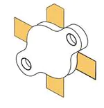
Figure 1: Pin connection
)
s
t(
1 (drain)
c
u
d
4 (source)
e
t
le
o
s
b
o
r
P
-O
2 (source)
The STAC250V2-500E uses the latest RF Power
SuperDMOS technology specially designed for
150 V and 250 V industrial RF power Class-AB,
C, D and E generators such as PECVD, plasma
sputtering, flat panel and solar cell manufacturing
equipment. The STAC250V2-500E benefits from
the latest generation of STAC® air cavity
packaging, which exhibits a 25% lower thermal
resistance compared to equivalent ceramic
packages.
3 (gate)
5 (source) on
backside
O
Table 1: Device summary
Order code
Marking
Package
Packing
STAC250V2-500E
250V2-500 (1)
STAC177B
Plastic tray
Notes:
(1)For
more details please refer to Section 6: "Marking, packing and shipping specifications" .
October 2015
DocID026071 Rev 6
This is information on a product in full production.
1/14
www.st.com
�Contents
STAC250V2-500E
Contents
1
Electrical data .................................................................................. 3
2
1.1
Maximum ratings ............................................................................... 3
1.2
Thermal data ..................................................................................... 3
3
Electrical characteristics ................................................................ 4
2.1
Static ................................................................................................. 4
2.2
Dynamic ............................................................................................ 4
Impedance data ............................................................................... 6
)
s
t( 10
Package information .....................................................................
c
u
d
o
r
Marking, packing and shipping specifications............................
12
P
Revision history ............................................................................
13
e
t
le
o
s
b
O
)
s
t(
c
u
d
o
r
P
e
t
e
l
so
4
5
Typical performance ....................................................................... 7
5.1
6
7
STAC177B package information ..................................................... 10
Ob
2/14
DocID026071 Rev 6
�STAC250V2-500E
Electrical data
1
Electrical data
1.1
Maximum ratings
(TCASE = 25 °C)
Table 2: Absolute maximum ratings
Symbol
Value
Unit
V(BR)DSS
Drain-source voltage
1000
V
VGS
Gate-source voltage
± 20
V
Max. operating junction temperature
200
TJ
TSTG
1.2
Parameter
Storage temperature
-65 to +150
t
c
u
d
o
r
Thermal data
P
e
et
Table 3: Thermal data
Symbol
RthJC
Parameter
Junction-case thermal resistance
)
s
t(
)
s
(
l
o
s
°C
°C
Value
Unit
0.14
°C/W
b
O
-
c
u
d
e
t
le
o
r
P
o
s
b
O
DocID026071 Rev 6
3/14
�Electrical characteristics
2
STAC250V2-500E
Electrical characteristics
TCASE = +25 oC
2.1
Static
Table 4: Static
Symbol
Test conditions
V(BR)DSS
2.2
IDS = 250 µ A
1
IGSS
VGS = 20 V; VDS = 0 V
1
VTH
ID = 250 µ A
3
VGS = 10 V ; ID = 7 A
4.2
GFS
VDS = 7 V ; ID = 3.5 A
4.4
CISS
VGS = 0 V; VDS = 150 V ; f = 1 MHz
COSS
VGS = 0 V; VDS = 150 V ; f = 1 MHz
CRSS
VGS = 0 V; VDS = 150 V ; f = 1 MHz
POUT
Gain
P
e
et
Efficiency
5
µA
V
V
S
pF
140
pF
1
pF
eP
t
e
l
o
s
b
O
Table 5: Dynamic
Test conditions
Typ.
Max.
VDD = 150 V, PIN = 3 W
500
520
-
VDD = 250 V, PIN = 2.4 W
500
700
-
VDD = 150 V, PIN = 3 W
22
22.3
-
VDD = 250 V, PIN = 2.4 W
24
24.6
-
VDD = 150 V, POUT = 3 W
70
73
-
%
VDD = 250 V, POUT = 2.4 W
70
74
Unit
-
%
W
dB
(1)
VDD = 150 V, POUT = 500 W
10:1
65:1
-
VDD = 250 V, POUT = 500 W
6:1
20:1(1)
-
Load mismatch
(1)Under
t
c
u
)
s
(
Min.
t
c
u
d
o
r
6
µA
d
o
r
980
Notes:
4/14
4.7
VDS(ON)
)
(s
Unit
V
VGS = 0 V; VDS = 750 V
Symbol
O
Max.
IDSS
Frequency = 13.56 MHz Class-C
bs
Typ.
1000
Dynamic
ol
Min.
pulse conditions: 1 ms - 10%.
DocID026071 Rev 6
VSWR
�STAC250V2-500E
Electrical characteristics
Table 6: Dynamic (frequency = 13.56 MHz Class-AB, Idq = 25 mA)
Symbol
Test conditions
POUT
Gain
Efficiency
Min.
Typ.
Max.
Unit
VDD = 150 V, PIN = 1 W
500
580
-
VDD = 250 V, PIN = 0.5 W
500
700
-
VDD = 150 V, PIN = 1 W
27
27.6
-
VDD = 250 V, PIN = 0.5 W
30
31
-
VDD = 150 V, PIN = 1 W
70
73
-
%
VDD = 250 V, PIN = 0.5
70
75
-
%
W
dB
(1)
VDD = 150 V, POUT = 500 W
6:1
65:1
-
VDD = 250 V, POUT = 500 W
5:1
20:1(1)
-
Load mismatch
VSWR
c
u
d
Notes:
(1)Under
)
s
t(
pulse conditions: 1 ms - 10%.
e
t
le
o
r
P
o
s
b
O
)
s
(
t
c
u
d
o
r
P
e
t
e
l
o
s
b
O
DocID026071 Rev 6
5/14
�Impedance data
3
STAC250V2-500E
Impedance data
Figure 2: Impedance data
)
s
t(
c
u
d
e
t
le
o
r
P
Table 7: Impedance values
Frequency (MHz)
Zin
13.56
4.6 + j 3.2
)
s
t(
so
Zdl (150 V)
b
O
-
36 + j 18
c
u
d
e
t
le
o
r
P
o
s
b
O
6/14
DocID026071 Rev 6
Zdl (180 V)
Zdl (250 V)
39 + j 22
44 + j 56
�STAC250V2-500E
4
Typical performance
Typical performance
Figure 3: Capacitance vs. drain-source voltage
1,000,000
100,000
Capacitance (pF)
10,000
1,000
Ciss
100
Coss
)
s
t(
c
u
d
10
1
e
t
le
0
0.1
1
10
o
r
P
100
Drain-source voltage (V)
so
b
O
-
Crss
1000
GIPG100220141622FSR
Figure 4: Gain vs. output power and supply voltage (frequency = 13.56 MHz Class-C)
Gain (dB)
150 V
e
t
le
O
o
s
b
)
s
t(
29
28
27
26
25
24
23
22
21
20
19
18
17
180 V
250 V
c
u
d
o
r
P
0
100
200
300
400
500
600
700
800
Output power (W)
DocID026071 Rev 6
7/14
�Typical performance
STAC250V2-500E
Figure 5: Efficiency vs. output power and supply voltage (frequency = 13.56 MHz Class-C)
150 V
180 V
250 V
100
90
80
Efficiency (%)
70
60
50
40
30
20
)
s
t(
10
0
0
100
200
300
400
500
600
uc
700
d
o
r
Output power (W)
800
P
e
et
Figure 6: Gain vs. output power and supply voltage (frequency = 13.56 MHz Class-AB,
Idq = 25 mA)
Gain (dB)
150 V
e
t
le
o
s
b
O
8/14
40
39
38
37
36
35
34
33
32
31
30
29
28
27
26
25
)
s
t(
180 V
l
o
s
250 V
b
O
-
c
u
d
o
r
P
0
100
200
300
400
500
Output power (W)
DocID026071 Rev 6
600
700
800
�STAC250V2-500E
Typical performance
Figure 7: Efficiency vs. output power and supply voltage (frequency = 13.56 MHz Class-AB,
Idq = 25 mA)
150 V
180 V
250 V
100
90
80
Efficiency (%)
70
60
50
40
)
s
t(
30
20
c
u
d
10
0
0
100
200
300
400
500
ro
600
P
e
et
Output power (W)
700
800
l
o
s
)
s
t(
b
O
-
c
u
d
e
t
le
o
r
P
o
s
b
O
DocID026071 Rev 6
9/14
�Package information
5
STAC250V2-500E
Package information
In order to meet environmental requirements, ST offers these devices in different grades of
ECOPACK® packages, depending on their level of environmental compliance. ECOPACK®
specifications, grade definitions and product status are available at: www.st.com.
ECOPACK is an ST trademark.
5.1
STAC177B package information
Figure 8: STAC177B package outline
)
s
t(
c
u
d
e
t
le
o
r
P
o
s
b
O
)
s
(
t
c
u
d
o
r
P
e
t
e
l
o
s
b
O
8334044_A
10/14
DocID026071 Rev 6
�STAC250V2-500E
Package information
Table 8: STAC177B package mechanical data
mm
Dim.
Min.
Typ.
Max.
A
5.72
5.97
B
6.73
6.99
C
21.84
22.10
D
28.70
28.96
E
28.02
F
0.10
0.15
G
0.81
)
s
t(
H
1.45
1.70
I
5.79
6.15
J
27.43
K
15.01
uc
28.45
od
r
P
e
15.27
t
e
l
o
)
(s
s
b
O
t
c
u
d
o
r
P
e
et
l
o
s
Ob
DocID026071 Rev 6
11/14
�Marking, packing and shipping specifications
6
STAC250V2-500E
Marking, packing and shipping specifications
Table 9: Packing and shipping specifications
Order code
Packaging
Pieces per tray
Dry pack humidity
Lot code
STAC250V2-500E
Plastic tray
25
< 10%
Not mixed
Figure 9: Marking layout
)
s
t(
c
u
d
e
t
le
o
r
P
o
s
b
O
)
s
(
t
c
Table 10: Marking specifications
Symbol
u
d
o
CZ
r
P
e
xxx
VY
t
e
l
o
s
b
O
12/14
MAR
CZ
Assembly plant
Last 3 digits of diffusion lot
Diffusion plant
Country of origin
Test and finishing plant
y
Assembly year
yy
Assembly week
DocID026071 Rev 6
Description
�STAC250V2-500E
7
Revision history
Revision history
Table 11: Document revision history
Date
Revision
14-Mar-2014
1
Initial release.
04-Aug-2014
2
Modified title in cover page.
Updated static table.
Minor text change
15-Sep-2014
3
Document status promoted from preliminary to production data.
10-Nov-2014
4
Updated title and features in cover page.
5
Updated features and description in cover page. Updated electrical
data section.
Updated the dynamic table, the table of impedance values and
V(BR)DSS parameter in the static table.
Changed figures of the typical performance section. Updated
package information section.
6
Changed Figure 4: "Gain vs. output power and supply voltage
(frequency = 13.56 MHz Class-C)" and Figure 5: "Efficiency vs.
output power and supply voltage (frequency = 13.56 MHz Class-C) "
Added Figure 6: "Gain vs. output power and supply voltage
(frequency = 13.56 MHz Class-AB, Idq = 25 mA)" and Figure 7: "
Efficiency vs. output power and supply voltage (frequency = 13.56
MHz Class-AB, Idq = 25 mA)".
07-Oct-2015
15-Oct-2015
Changes
)
s
t(
c
u
d
e
t
le
o
r
P
o
s
b
O
)
s
(
t
c
u
d
o
r
P
e
t
e
l
o
s
b
O
DocID026071 Rev 6
13/14
�STAC250V2-500E
IMPORTANT NOTICE – PLEASE READ CAREFULLY
STMicroelectronics NV and its subsidiaries (“ST”) reserve the right to make changes, corrections, enhancements, modifications, and
improvements to ST products and/or to this document at any time without notice. Purchasers should obtain the latest relevant information on ST
products before placing orders. ST products are sold pursuant to ST’s terms and conditions of sale in place at the time of order
acknowledgement.
Purchasers are solely responsible for the choice, selection, and use of ST products and ST assumes no liability for application assistance or the
design of Purchasers’ products.
)
s
t(
No license, express or implied, to any intellectual property right is granted by ST herein.
c
u
d
Resale of ST products with provisions different from the information set forth herein shall void any warranty granted by ST for such product.
o
r
P
ST and the ST logo are trademarks of ST. All other product or service names are the property of their respective owners.
e
t
le
Information in this document supersedes and replaces information previously supplied in any prior versions of this document.
o
s
b
© 2015 STMicroelectronics – All rights reserved
O
)
s
(
t
c
u
d
o
r
P
e
t
e
l
o
s
b
O
14/14
DocID026071 Rev 6
�