STAC2942F
HF/VHF/UHF RF power N-channel MOSFETs
Features
■
Gold metallization
■
Excellent thermal stability
■
Common source push-pull configuration
■
POUT = 350 W min. with 21 dB gain @ 175 MHz
■
In compliance with the 2002/95/EC European
directive
Description
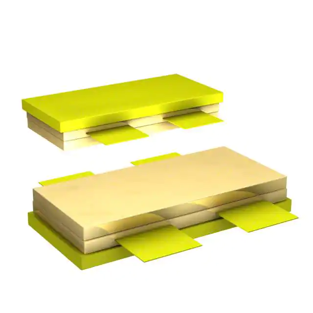
STAC244F
Air cavity
The STAC2942F is a gold metallized N-channel
MOS field-effect RF power transistor. It is
intended for use in 50 V DC large signal
applications up to 250 MHz.
Figure 1.
Pin connection
1
1
2
2
Table 1.
3
1. Drain
3. Source
2. Gate
(Bottom side)
Device summary
Order code
Marking
Package
Packaging
STAC2942FW
STAC2942F(1)
STAC244F
Plastic tray
1. For more details please refer to Chapter 7: Marking, packing and shipping specifications.
October 2011
Doc ID 17122 Rev 3
1/16
www.st.com
16
�Contents
STAC2942F
Contents
1
2
Electrical data . . . . . . . . . . . . . . . . . . . . . . . . . . . . . . . . . . . . . . . . . . . . . . 3
1.1
Maximum ratings . . . . . . . . . . . . . . . . . . . . . . . . . . . . . . . . . . . . . . . . . . . . 3
1.2
Thermal data . . . . . . . . . . . . . . . . . . . . . . . . . . . . . . . . . . . . . . . . . . . . . . . 3
Electrical characteristics . . . . . . . . . . . . . . . . . . . . . . . . . . . . . . . . . . . . . 4
2.1
Static . . . . . . . . . . . . . . . . . . . . . . . . . . . . . . . . . . . . . . . . . . . . . . . . . . . . . 4
2.2
Dynamic . . . . . . . . . . . . . . . . . . . . . . . . . . . . . . . . . . . . . . . . . . . . . . . . . . . 4
3
Impedance . . . . . . . . . . . . . . . . . . . . . . . . . . . . . . . . . . . . . . . . . . . . . . . . . 5
4
Typical performance . . . . . . . . . . . . . . . . . . . . . . . . . . . . . . . . . . . . . . . . . 6
5
Test circuit . . . . . . . . . . . . . . . . . . . . . . . . . . . . . . . . . . . . . . . . . . . . . . . . 10
6
Package mechanical data . . . . . . . . . . . . . . . . . . . . . . . . . . . . . . . . . . . . 12
7
Marking, packing and shipping specifications . . . . . . . . . . . . . . . . . . . 14
8
Revision history . . . . . . . . . . . . . . . . . . . . . . . . . . . . . . . . . . . . . . . . . . . 15
2/16
Doc ID 17122 Rev 3
�STAC2942F
Electrical data
1
Electrical data
1.1
Maximum ratings
Table 2.
Absolute maximum ratings (TCASE = 25 °C)
Symbol
V(BR)DSS(1)
VDGR
(1)
VGS
ID
PDISS
TJ
TSTG
Parameter
Value
Unit
Drain source voltage
130
V
Drain-gate voltage (RGS = 1 MΩ)
130
V
Gate-source voltage
±20
V
Drain current
40
A
Power dissipation
625
W
Max. operating junction temperature
200
°C
-65 to +150
°C
Value
Unit
0.28
°C/W
Storage temperature
1. TJ = 150 °C
1.2
Thermal data
Table 3.
Symbol
RthJC
Thermal data
Parameter
Junction - case thermal resistance
Doc ID 17122 Rev 3
3/16
�Electrical characteristics
2
STAC2942F
Electrical characteristics
(TCASE = 25 oC)
2.1
Static
Table 4.
Static (per side)
Symbol
Test conditions
V(BR)DSS(1) VGS = 0 V
Min.
IDS = 100 mA
Typ.
Max.
130
Unit
V
IDSS
VGS = 0 V
VDS = 50 V
100
µA
IGSS
VGS = 20 V
VDS = 0 V
250
nA
VGS(Q)
VDS = 10 V
ID = 250 mA
4.0
V
VDS(ON)
VGS = 10 V
ID = 10 A
3.0
V
GFS
VDS = 10 V
ID = 5 A
1.5
5
CISS
COSS
VGS = 0 V
VDS = 50 V
2.5
f = 1 MHz
CRSS
S
425
pF
202
pF
12
pF
1. TJ = 150 °C
2.2
Dynamic
Table 5.
Symbol
4/16
Dynamic
Test conditions
Min.
Typ.
Max.
Unit
POUT
VDD = 50 V, IDQ = 2 x 250 mA, PIN = 4 W, f = 175 MHz
350
450
W
hD
VDD = 50 V, IDQ = 2 x 250 mA, PIN = 4 W, f = 175 MHz
60
75
%
Doc ID 17122 Rev 3
�STAC2942F
3
Note:
Impedance
Impedance
Figure 2.
Current conventions
Table 6.
Impedance data
Freq. (MHz)
ZIN (Ω)
ZDL(Ω)
175 MHz
2.0 - j2.0
3.5 + j5.2
Measured gate to gate and drain to drain, respectively.
Doc ID 17122 Rev 3
5/16
�Typical performance
4
STAC2942F
Typical performance
Figure 3.
Capacitances vs drain supply Figure 4.
voltage
AM00556v1
1000
$0�����Y�
���
)UHT�� �����0+]��,GT� ��[�����P$
Freq. = 1 MHz
900
Output power vs drain supply
voltage
���
3LQ� �����:
���
800
3LQ� ��:
���
2XWSXW�SRZHU��:�
Capacitances (pF)
700
Ciss
Crss
600
Coss
500
A M 0 0 5 5 6
400
3LQ� ����:
���
���
���
���
���
300
���
200
���
100
��
�
0
0
10
20
30
40
50
��
60
��
Supply voltage (V)
Figure 5.
Output power vs gate voltage Figure 6.
��
!-�����V�
���
���
���
&REQ����-(Z
0IN����7
6DD���6
)DQ��X���M!
���
���
���
���
6DD���6
/UTPUTPOWER�7
���
���
���
4CASE���� #
���
4CASE���� #
���
��
Output power vs input power
!-�����V�
���
/UTPUTPOWER�7
��
6XSSO\�YROWDJH��9�
6DD���6
���
���
���
���
&REQ� ��� -(Z
)DQ��X���M!
4CASE�� �� #
���
4CASE�
�� #
���
���
���
��
��
�
�
�
���
�
���
�
���
�
���
�
���
'ATEVOLTAGE�6
6/16
Doc ID 17122 Rev 3
�
�
�
�
�
��
��
��
��
�STAC2942F
Typical performance
Figure 7.
Output power vs input power Figure 8.
and case temperature
!-�����V�
���
Efficiency vs output power
and case temperature
!-�����V�
���
���
&REQ����-(Z
6DD���6
)DQ��X���M!
��
���
��
���
��
%FFICIENCY��
/UTPUTPOWER�7
���
���
���
&REQ����-(Z
6DD���6
)DQ��X���M!
���
��
��
��
���
4CASE���� #
���
��
���
4CASE���� #
��
4CASE�
�� #
��
4CASE���� #
���
4CASE���� #
��
4CASE�
�� #
�
�
�
�
Figure 9.
�
�
�
��
)NPUT0OWER�7
��
��
��
�
���
���
���
���
/UTPUT0OWER�7
���
���
���
Power gain vs output power
and case temperature
!-�����V�
��
��
��
0OWERGAIN�D"
��
��
&REQ����-(Z
6DD���6
)DQ��X���M!
��
��
��
��
4CASE���� #
4CASE���� #
4CASE�
�� #
��
��
�
�� ��� ��� ��� ��� ��� ��� ��� ��� ��� ��� ��� ���
/UTPUT0OWER�7
Doc ID 17122 Rev 3
7/16
�Typical performance
STAC2942F
Figure 10. Maximum safe operating area
6ECUG���
��u%�����6L���
���u%
/CZ�&TCKP�%WTTGPV�� +F�
#�
����
���
&%
���O5
��O5
��
�
�
����
����
��
����
&TCKP�UWRRN[�XQNVCIG�� 8FF�
8�
!-�����V�
Figure 11. Transient thermal impedance
����
:THJ
C� #�7
����
3INGLEPULSE
���
����
���
���
����
���
���
� ��
���
���
���
����
��%
��
���
��%
��
��%
��
��%
��
��%���
2ECTANGULAR POWER PULSE WIDTH �SEC
!-�����V�
8/16
Doc ID 17122 Rev 3
�STAC2942F
Typical performance
Figure 12. Transient thermal model
2
2�
2 ���������� /HM
#
#�
# ���������� &
2
2�
2 ���������� /HM
#
#�
# ���������� &
2
2�
2 ��������� /HM
#
#�
# ���������� &
2
2�
2 ��������� /HM
#
#�
# ���������� &
!-�����V�
Doc ID 17122 Rev 3
9/16
�Test circuit
5
STAC2942F
Test circuit
Figure 13. 175 MHz test circuit schematic (production test circuit)
$
#
#
$
$
%
#
#
#
#
#
%
%
$
������«52#%' &+/'05+10«6#$.'
&+/
+0
//
#
$
�����
�����
�����
�����
%
�����
�����
#
%
64#05/+55+10«.+0'«&+/'05+105
($�
%��
($�
4�
%��
%�
($�
6�
%14'
$�
6�
%�
($�
%��
%14'
.+
%��
6GF
6�
%14'
%��
($�
4�
4�
%�
%�
%�
%��
%14'
�8II
%��
%��
%��
%��
%��
6�
%��
%��
($�
�8II
4�
($�
%��
4�
4�
%��
%��
%��
016'5�
��«&+/'05+105«#6«%1/210'06«5;/$1.5«#4'«4'('4'0%'«(14«%1/210'06«2.#%'/'06�«5''«5*''6«��
��«)#2«$'69''0«)4170&« «64#05/+55+10«.+0'5«+5«�����=����?«««««««««««««6;2
!-�����V�
Table 7.
175 MHz test circuit component part list
Component
Description
C1, C2, C14,
C15, C24, C25
1200 pF ATC 700B chip capacitor
C5
75 pF ATC 100B chip capacitor
C6
ST406 variable capacitor
C9, C10
47 pF ATC 100B chip capacitor
C11, C12, C13
43 pF ATC 100B chip capacitor
C16, C18
470 pF ATC 100B chip capacitor
C17, C19, C20, C21
10,000 pF ATC 200B chip capacitor
C22, C23
0.1 µF 200 V chip capacitor
C28
10 µF 100 V electrolytic capacitor
C29
0.8 - 8 pF variable capacitor
R1, R2, R5, R6
430 Ω, 1/2 W chip resistor
10/16
��8
Doc ID 17122 Rev 3
$�
%��
�STAC2942F
Table 7.
Test circuit
175 MHz test circuit component part list (continued)
Component
Description
R3, R4
270 Ω 1/2 W axial lead resistor
B1
RG-316 50 Ω 11.8" thru ferrite toroid
B2
RG-142 50 Ω 11.8"
T1
4:1, RG-316 25 Ω, 5.9", 2 turns thru ferrite core
T2
1:4, 25 Ω semi-rigid cable, OD .141", 5.9"
L1
λ/4 inductor, RG-142 50 Ω, 11.8", 3 turns thru ferrite toroid
FB1,FB5
Ferrite toroid
FB2, FB6
Multi-aperture core
FB3, FB4
Surface mount ferrite bead
PCB
Rogers ultralam 2000, Er 2.55, .060"
Figure 14. Circuit layout
Doc ID 17122 Rev 3
11/16
�Package mechanical data
6
STAC2942F
Package mechanical data
In order to meet environmental requirements, ST offers these devices in different grades of
ECOPACK® packages, depending on their level of environmental compliance. ECOPACK®
specifications, grade definitions and product status are available at: www.st.com.
ECOPACK® is an ST trademark.
Table 8.
STAC244F package dimensions
mm.
Inch
Dim.
12/16
Min
Max
Min
Max
A
5.10
5.59
200
220
A1
4.32
4.83
170
190
B
4.32
5.33
170
210
C
9.65
9.91
380
390
D
19.61
20.02
772
788
E
20.45
20.70
805
815
F
0.08
1.15
.003
.006
G
0.89
1.14
.035
.045
H
1.45
1.70
.057
.067
I
3.18
4.32
.125
.170
J
9.27
9.53
.365
.375
Doc ID 17122 Rev 3
�STAC2942F
Package mechanical data
Figure 15. Package dimensions
AM01112v1
Doc ID 17122 Rev 3
13/16
�Marking, packing and shipping specifications
7
STAC2942F
Marking, packing and shipping specifications
Table 9.
Packing and shipping specifications
Order code
Packaging
Pcs per tray
Dry pack
humidity
Lot code
STAC2942FW
Tube
20
< 10 %
Not mixed
Figure 16. Marking layout
STAC2942F
Table 10.
14/16
Marking specifications
Symbol
Description
W
Wafer process code
CZ
Assembly plant
xxx
Last 3 digit of diffusion lot
VY
Diffusion plant
MAR
Country of origin
CZ
Test and finishing plant
y
Assembly year
yy
Assembly week
Doc ID 17122 Rev 3
�STAC2942F
8
Revision history
Revision history
Table 11.
Document revision history
Date
Revision
Changes
12-Feb-2010
1
First release.
16-Apr-2010
2
Added Figure 10, Figure 11 and Figure 12.
25-Oct-2011
3
Added Chapter 7: Marking, packing and shipping specifications.
Doc ID 17122 Rev 3
15/16
�STAC2942F
Please Read Carefully:
Information in this document is provided solely in connection with ST products. STMicroelectronics NV and its subsidiaries (“ST”) reserve the
right to make changes, corrections, modifications or improvements, to this document, and the products and services described herein at any
time, without notice.
All ST products are sold pursuant to ST’s terms and conditions of sale.
Purchasers are solely responsible for the choice, selection and use of the ST products and services described herein, and ST assumes no
liability whatsoever relating to the choice, selection or use of the ST products and services described herein.
No license, express or implied, by estoppel or otherwise, to any intellectual property rights is granted under this document. If any part of this
document refers to any third party products or services it shall not be deemed a license grant by ST for the use of such third party products
or services, or any intellectual property contained therein or considered as a warranty covering the use in any manner whatsoever of such
third party products or services or any intellectual property contained therein.
UNLESS OTHERWISE SET FORTH IN ST’S TERMS AND CONDITIONS OF SALE ST DISCLAIMS ANY EXPRESS OR IMPLIED
WARRANTY WITH RESPECT TO THE USE AND/OR SALE OF ST PRODUCTS INCLUDING WITHOUT LIMITATION IMPLIED
WARRANTIES OF MERCHANTABILITY, FITNESS FOR A PARTICULAR PURPOSE (AND THEIR EQUIVALENTS UNDER THE LAWS
OF ANY JURISDICTION), OR INFRINGEMENT OF ANY PATENT, COPYRIGHT OR OTHER INTELLECTUAL PROPERTY RIGHT.
UNLESS EXPRESSLY APPROVED IN WRITING BY TWO AUTHORIZED ST REPRESENTATIVES, ST PRODUCTS ARE NOT
RECOMMENDED, AUTHORIZED OR WARRANTED FOR USE IN MILITARY, AIR CRAFT, SPACE, LIFE SAVING, OR LIFE SUSTAINING
APPLICATIONS, NOR IN PRODUCTS OR SYSTEMS WHERE FAILURE OR MALFUNCTION MAY RESULT IN PERSONAL INJURY,
DEATH, OR SEVERE PROPERTY OR ENVIRONMENTAL DAMAGE. ST PRODUCTS WHICH ARE NOT SPECIFIED AS "AUTOMOTIVE
GRADE" MAY ONLY BE USED IN AUTOMOTIVE APPLICATIONS AT USER’S OWN RISK.
Resale of ST products with provisions different from the statements and/or technical features set forth in this document shall immediately void
any warranty granted by ST for the ST product or service described herein and shall not create or extend in any manner whatsoever, any
liability of ST.
ST and the ST logo are trademarks or registered trademarks of ST in various countries.
Information in this document supersedes and replaces all information previously supplied.
The ST logo is a registered trademark of STMicroelectronics. All other names are the property of their respective owners.
© 2011 STMicroelectronics - All rights reserved
STMicroelectronics group of companies
Australia - Belgium - Brazil - Canada - China - Czech Republic - Finland - France - Germany - Hong Kong - India - Israel - Italy - Japan Malaysia - Malta - Morocco - Philippines - Singapore - Spain - Sweden - Switzerland - United Kingdom - United States of America
www.st.com
16/16
Doc ID 17122 Rev 3
�