STAC3933
RF power transistor:
HF/VHF/UHF RF power N-channel MOSFETs
Preliminary data
Features
■
Excellent thermal stability
■
Common source configuration
■
POUT = 350 W min. with 29 dB gain @ 30 MHz
■
STAC air cavity packaging technology STAC® package
Description
The STAC3933 is an N-channel MOS field-effect
RF power transistor, intended for use in 100 V DC
large signal applications up to 200 MHz.
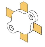
STAC177B
Figure 1.
Pin connection
1 (drain)
2 (source)
4 (source)
3 (gate)
5 (source) on
backside
Table 1.
Device summary
Order code
Marking
Base qty.
Package
Packaging(1)
STAC3933
STAC3933(1)
25 pcs
STAC177B
Plastic tray
1. For more details please refer to Chapter 6: Marking, packing and shipping specifications..
January 2012
Doc ID 022696 Rev 1
This is preliminary information on a new product now in development or undergoing evaluation. Details are subject to
change without notice.
1/14
www.st.com
14
�Contents
STAC3933
Contents
1
2
Electrical data . . . . . . . . . . . . . . . . . . . . . . . . . . . . . . . . . . . . . . . . . . . . . . 3
1.1
Maximum ratings . . . . . . . . . . . . . . . . . . . . . . . . . . . . . . . . . . . . . . . . . . . . 3
1.2
Thermal data . . . . . . . . . . . . . . . . . . . . . . . . . . . . . . . . . . . . . . . . . . . . . . . 3
Electrical characteristics . . . . . . . . . . . . . . . . . . . . . . . . . . . . . . . . . . . . . 4
2.1
Static . . . . . . . . . . . . . . . . . . . . . . . . . . . . . . . . . . . . . . . . . . . . . . . . . . . . . 4
2.2
Dynamic . . . . . . . . . . . . . . . . . . . . . . . . . . . . . . . . . . . . . . . . . . . . . . . . . . . 4
3
Impedance data . . . . . . . . . . . . . . . . . . . . . . . . . . . . . . . . . . . . . . . . . . . . . 8
4
Typical performance . . . . . . . . . . . . . . . . . . . . . . . . . . . . . . . . . . . . . . . . . 9
5
Package mechanical data . . . . . . . . . . . . . . . . . . . . . . . . . . . . . . . . . . . . 10
6
Marking, packing and shipping specifications . . . . . . . . . . . . . . . . . . . 12
7
Revision history . . . . . . . . . . . . . . . . . . . . . . . . . . . . . . . . . . . . . . . . . . . 13
2/14
Doc ID 022696 Rev 1
�STAC3933
Electrical data
1
Electrical data
1.1
Maximum ratings
(TCASE = 25 °C)
Table 2.
Absolute maximum ratings
Symbol
Value
Unit
Drain source voltage
250
V
Drain-gate voltage (RGS = 1 MΩ)
250
V
Gate-source voltage
±20
V
Drain current
20
A
Power dissipation
795
W
EAS
Avalanche energy
Single pulse (ID = 50 A - 800 µH coil)
1000
mJ
TJ
Max. operating junction temperature
200
°C
-65 to +150
°C
Value
Unit
0.22
°C/W
V(BR)DSS(1)
VDGR
VGS
ID
PDISS
TSTG
Parameter
Storage temperature
1. TJ = 150 °C
1.2
Thermal data
Table 3.
Symbol
RthJC
Thermal data
Parameter
Junction - case thermal resistance
Doc ID 022696 Rev 1
3/14
�Electrical characteristics
2
STAC3933
Electrical characteristics
TCASE = +25 oC
2.1
Static
Table 4.
Static
Symbol
V(BR)DSS(1) VGS = 0 V
Test conditions
Min
IDS = 100 mA
250
IDSS
VGS = 0 V
VDS = 100 V
IGSS
VGS = 20 V
VDS = 0 V
VGS(Q)
VDS = 10 V
ID = 250 mA
VDS(ON)
VGS = 10 V
ID = 10 A
GFS
VDS = 10 V
ID = 5 A
CISS
VGS = 0 V
VDS = 100 V
COSS
VGS = 0 V
CRSS
VGS = 0 V
1.5
5
Typ
Max
Unit
V
2
mA
500
nA
2.5
4.0
V
2.5
3.5
V
8
S
f = 1 MHz
1000
pF
VDS = 100 V
f = 1 MHz
265
pF
VDS = 100 V
f = 1 MHz
13
pF
1. TJ = +150 °C
2.2
Dynamic
Table 5.
Dynamic
Symbol
4/14
Test conditions
Min
Typ
Max
Unit
POUT
VDD = 100 V
IDQ = 250 mA
f = 30 MHz
350
GPS
VDD = 100 V
IDQ = 250 mA POUT = 350 W f = 30 MHz
25
29
dB
hD
VDD = 100 V
IDQ = 250 mA POUT = 350 W f = 30 MHz
60
66
%
VDD = 100 V IDQ = 250 mA POUT = 300 W f = 30 MHz
Load
mismatch all phase angles
3:1
Doc ID 022696 Rev 1
W
VSWR
�STAC3933
Electrical characteristics
Table 6.
VGS/GFS sorts
Marking
Vgs(min)
Vgs(max)
Gfs(min)
Gfs(max)
A1
1.50
1.75
5
6
A2
1.50
1.75
6
7
A3
1.50
1.75
7
8
A4
1.50
1.75
8
9
A5
1.50
1.75
9
10
A6
1.50
1.75
10
11
A7
1.50
1.75
11
12
A8
1.50
1.75
12
13
A9
1.50
1.75
13
14
B1
1.75
2.00
5
6
B2
1.75
2.00
6
7
B3
1.75
2.00
7
8
B4
1.75
2.00
8
9
B5
1.75
2.00
9
10
B6
1.75
2.00
10
11
B7
1.75
2.00
11
12
B8
1.75
2.00
12
13
B9
1.75
2.00
13
14
C1
2.00
2.25
5
6
C2
2.00
2.25
6
7
C3
2.00
2.25
7
8
C4
2.00
2.25
8
9
C5
2.00
2.25
9
10
C6
2.00
2.25
10
11
C7
2.00
2.25
11
12
C8
2.00
2.25
12
13
C9
2.00
2.25
13
14
D1
2.25
2.50
5
6
D2
2.25
2.50
6
7
D3
2.25
2.50
7
8
D4
2.25
2.50
8
9
D5
2.25
2.50
9
10
D6
2.25
2.50
10
11
D7
2.25
2.50
11
12
Doc ID 022696 Rev 1
5/14
�Electrical characteristics
Table 6.
6/14
STAC3933
VGS/GFS sorts (continued)
Marking
Vgs(min)
Vgs(max)
Gfs(min)
Gfs(max)
D8
2.25
2.50
12
13
D9
2.25
2.50
13
14
E1
2.50
2.75
5
6
E2
2.50
2.75
6
7
E3
2.50
2.75
7
8
E4
2.50
2.75
8
9
E5
2.50
2.75
9
10
E6
2.50
2.75
10
11
E7
2.50
2.75
11
12
E8
2.50
2.75
12
13
E9
2.50
2.75
13
14
F1
2.75
3.00
5
6
F2
2.75
3.00
6
7
F3
2.75
3.00
7
8
F4
2.75
3.00
8
9
F5
2.75
3.00
9
10
F6
2.75
3.00
10
11
F7
2.75
3.00
11
12
F8
2.75
3.00
12
13
F9
2.75
3.00
13
14
G1
3.00
3.25
5
6
G2
3.00
3.25
6
7
G3
3.00
3.25
7
8
G4
3.00
3.25
8
9
G5
3.00
3.25
9
10
G6
3.00
3.25
10
11
G7
3.00
3.25
11
12
G8
3.00
3.25
12
13
G9
3.00
3.25
13
14
H1
3.25
3.50
5
6
H2
3.25
3.50
6
7
H3
3.25
3.50
7
8
H4
3.25
3.50
8
9
H5
3.25
3.50
9
10
H6
3.25
3.50
10
11
Doc ID 022696 Rev 1
�STAC3933
Electrical characteristics
Table 6.
VGS/GFS sorts (continued)
Marking
Vgs(min)
Vgs(max)
Gfs(min)
Gfs(max)
H7
3.25
3.50
11
12
H8
3.25
3.50
12
13
H9
3.25
3.50
13
14
I1
3.50
3.75
5
6
I2
3.50
3.75
6
7
I3
3.50
3.75
7
8
I4
3.50
3.75
8
9
I5
3.50
3.75
9
10
I6
3.50
3.75
10
11
I7
3.50
3.75
11
12
I8
3.50
3.75
12
13
I9
3.50
3.75
13
14
J1
3.75
4.00
5
6
J2
3.75
4.00
6
7
J3
3.75
4.00
7
8
J4
3.75
4.00
8
9
J5
3.75
4.00
9
10
J6
3.75
4.00
10
11
J7
3.75
4.00
11
12
J8
3.75
4.00
12
13
J9
3.75
4.00
13
14
Doc ID 022696 Rev 1
7/14
�Impedance data
3
STAC3933
Impedance data
Figure 2.
Impedance data
D
ZDL
Typical Input
Impedance
Typical Drain
Load Impedance
G
Zin
S
Table 7.
8/14
Impedance data (350 W load line)
Frequency
ZIN (Ω)
ZDL (Ω)
10 MHz
6.56 - j9.75
12.17 + j2.76
20 MHz
2.80 - j5.78
10.6 + j4.81
30 MHz
1.96 - j3.90
8.73 + j5.94
40 MHz
1.69 - j2.89
7.00 + j6.35
50 MHz
1.59 - j2.30
5.58 + j6.32
60 MHz
1.55 - j1.93
4.47 + j6.06
70 MHz
1.55 - j1.71
3.62 + j5.72
80 MHz
1.54 - j1.58
2.97 + j5.35
90 MHz
1.53 - j1.50
2.46 + j4.99
100 MHz
1.52 - j1.45
2.07 + j4.65
Doc ID 022696 Rev 1
�STAC3933
Typical performance
4
Typical performance
Figure 3.
Capacitance vs. supply voltage
3000
Crss
2750
Coss
Figure 4.
15
Ciss
14
13
2500
12
2250
11
2000
10
1750
9
1500
Ids (A)
Capacitance (pF)
Drain current vs. gate source
voltage
F = 1 MHz
1250
8
7
6
1000
5
750
4
500
3
250
2
0
1
0
20
40
60
80
100
Tc = +25 °C
Vds = 100 V
0
120
0
1
2
Vdd (V)
Figure 5.
Drain current vs. drain source
voltage
Figure 6.
1.6
10
1.4
Vgs (V), Normalized
12
8
Ids (A)
3
4
5
Vgs(V)
6
4
2
Gate source voltage vs. case
temperature
1.2
1.0
0.8
0.6
Tc = +25 °C
Vgs = 10 V
Idq = 250 mA
0
0.4
0.0
0.5
1.0
1.5
2.0
2.5
3.0
-50
Vds (V)
-25
0
25
50
75
100
Tc (°C)
Doc ID 022696 Rev 1
9/14
�Package mechanical data
5
STAC3933
Package mechanical data
In order to meet environmental requirements, ST offers these devices in different grades of
ECOPACK® packages, depending on their level of environmental compliance. ECOPACK®
specifications, grade definitions and product status are available at: www.st.com.
ECOPACK® is an ST trademark.
Table 8.
STAC177B mechanical data
mm
inch
Dim
Min.
Max.
Min.
Typ.
Max.
A
5.72
5.97
0.225
0.235
B
6.73
6.99
0.265
0.275
C
21.84
22.10
0.860
0.870
D
28.70
28.96
1.130
1.140
E
F
28.02
0.10
G
10/14
Typ.
1.103
0.15
0.004
0.81
0.006
0.032
H
1.45
1.70
0.057
0.067
I
5.79
6.15
0.228
0.242
J
27.43
28.45
1.080
1.120
K
15.01
15.27
0.591
0.601
Doc ID 022696 Rev 1
�STAC3933
Package mechanical data
Figure 7.
STAC177B mechanical drawing
8334044_A
Doc ID 022696 Rev 1
11/14
�Marking, packing and shipping specifications
6
Marking, packing and shipping specifications
Table 9.
12/14
STAC3933
Packing and shipping specifications
Order code
Packaging
Pcs per
tray
Dry pack
humidity
VGS and GFS
code
Lot code
STAC3933
Plastic tray
25
< 10 %
Not mixed
Not mixed
Figure 8.
Marking layout
Table 10.
Marking specifications
Symbol
Description
XX
VGS and GFS sort
CZ
Assembly plant
xxx
Last 3 digit of diffusion lot
VY
Diffusion plant
MAR
Country of origin
CZ
Test and finishing plant
y
Assembly year
yy
Assembly week
Doc ID 022696 Rev 1
�STAC3933
7
Revision history
Revision history
Table 11.
Document revision history
Date
Revision
17-Jan-2012
1
Changes
First release.
Doc ID 022696 Rev 1
13/14
�STAC3933
Please Read Carefully:
Information in this document is provided solely in connection with ST products. STMicroelectronics NV and its subsidiaries (“ST”) reserve the
right to make changes, corrections, modifications or improvements, to this document, and the products and services described herein at any
time, without notice.
All ST products are sold pursuant to ST’s terms and conditions of sale.
Purchasers are solely responsible for the choice, selection and use of the ST products and services described herein, and ST assumes no
liability whatsoever relating to the choice, selection or use of the ST products and services described herein.
No license, express or implied, by estoppel or otherwise, to any intellectual property rights is granted under this document. If any part of this
document refers to any third party products or services it shall not be deemed a license grant by ST for the use of such third party products
or services, or any intellectual property contained therein or considered as a warranty covering the use in any manner whatsoever of such
third party products or services or any intellectual property contained therein.
UNLESS OTHERWISE SET FORTH IN ST’S TERMS AND CONDITIONS OF SALE ST DISCLAIMS ANY EXPRESS OR IMPLIED
WARRANTY WITH RESPECT TO THE USE AND/OR SALE OF ST PRODUCTS INCLUDING WITHOUT LIMITATION IMPLIED
WARRANTIES OF MERCHANTABILITY, FITNESS FOR A PARTICULAR PURPOSE (AND THEIR EQUIVALENTS UNDER THE LAWS
OF ANY JURISDICTION), OR INFRINGEMENT OF ANY PATENT, COPYRIGHT OR OTHER INTELLECTUAL PROPERTY RIGHT.
UNLESS EXPRESSLY APPROVED IN WRITING BY TWO AUTHORIZED ST REPRESENTATIVES, ST PRODUCTS ARE NOT
RECOMMENDED, AUTHORIZED OR WARRANTED FOR USE IN MILITARY, AIR CRAFT, SPACE, LIFE SAVING, OR LIFE SUSTAINING
APPLICATIONS, NOR IN PRODUCTS OR SYSTEMS WHERE FAILURE OR MALFUNCTION MAY RESULT IN PERSONAL INJURY,
DEATH, OR SEVERE PROPERTY OR ENVIRONMENTAL DAMAGE. ST PRODUCTS WHICH ARE NOT SPECIFIED AS "AUTOMOTIVE
GRADE" MAY ONLY BE USED IN AUTOMOTIVE APPLICATIONS AT USER’S OWN RISK.
Resale of ST products with provisions different from the statements and/or technical features set forth in this document shall immediately void
any warranty granted by ST for the ST product or service described herein and shall not create or extend in any manner whatsoever, any
liability of ST.
ST and the ST logo are trademarks or registered trademarks of ST in various countries.
Information in this document supersedes and replaces all information previously supplied.
The ST logo is a registered trademark of STMicroelectronics. All other names are the property of their respective owners.
© 2012 STMicroelectronics - All rights reserved
STMicroelectronics group of companies
Australia - Belgium - Brazil - Canada - China - Czech Republic - Finland - France - Germany - Hong Kong - India - Israel - Italy - Japan Malaysia - Malta - Morocco - Philippines - Singapore - Spain - Sweden - Switzerland - United Kingdom - United States of America
www.st.com
14/14
Doc ID 022696 Rev 1
�
很抱歉,暂时无法提供与“STAC3933”相匹配的价格&库存,您可以联系我们找货
免费人工找货- 国内价格 香港价格
- 50+888.0109050+113.89694