STAC4932B
Datasheet
HF/VHF/UHF RF power N-channel MOSFET
Features
1
1
2
3
3
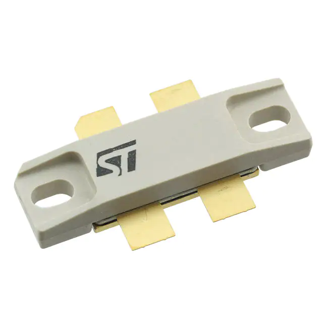
STAC780-4B
Pin connection
Pin
Connection
1
Drain
2
Source (bottom side)
3
Gate
Order code
Frequency
VDD
POUT
Gain
Efficiency
STAC4932B
123 MHz
100 V
1000 W
24.6 dB
60 %
•
•
•
Excellent thermal stability
Common source push-pull configuration
POUT = 1000 W min. (1200 W typ.) with 24.6 dB gain at 123 MHz
•
•
•
Pulse conditions: 1ms, 10%
In compliance with the 2002/95/EC European directive
ST air-cavity STAC package technology
Description
The STAC4932B is an N-channel MOS field-effect RF power transistor. It is intended
for 100 V pulse applications up to 250 MHz. This device is suitable for use in
industrial, scientific and medical applications. The STAC4932B benefits from the
latest generation of efficient, patent-pending STAC package technology.
Product status
STAC4932B
Product summary
Order code
STAC4932B
Marking
STAC4932
Package
STAC780-4B
Packing
Box
Base / Bulk qty
20 / 80
DS6724 - Rev 8 - April 2020
For further information contact your local STMicroelectronics sales office.
www.st.com
�STAC4932B
Electrical data
1
Electrical data
1.1
Maximum ratings
Table 1. Absolute maximum ratings (TCASE = 25 °C)
Symbol
V(BR)DSS
V DGR
V GS
TJ
T STG
1.2
Parameter
Value
Unit
Drain source voltage (VGS = 0 V, TJ = 150 °C)
200
V
Drain-gate voltage (R GS= 1 MΩ)
200
V
Gate-source voltage
±20
V
Maximum operating junction temperature
200
°C
-65 to +150
°C
Value
Unit
0.075
°C/W
Storage temperature range
Thermal data
Table 2. Thermal data (1ms, 10%)
Symbol
R thJC
1.3
Parameter
Junction - case thermal resistance
ESD protection characteristics
Table 3. ESD protection
Symbol
HBM
DS6724 - Rev 8
Test Methodology
Human Body Model (per JESD22-A114)
Class
2
page 2/13
�STAC4932B
Electrical characteristics
2
Electrical characteristics
( TCASE= +25 °C, unless otherwise noted)
2.1
Static
Table 4. Static
Symbol
V(BR)DSS
Drain-source breakdown
voltage
Test conditions
VGS = 0 V, IDS = 100 mA,
TJ = 150 °C
Min.
Typ.
200
250
Max.
Unit
V
IDSS
Zero gate voltage drain
leakage current
VGS = 0 V, VDS = 100 V
1
mA
IGSS
Gate-source leakage current
VGS = 20 V, VDS = 0 V
250
nA
Drain-source on voltage
VGS = 10 V, ID = 10 A
3.6
V
VTH
Gate-source threshold
voltage
IDS = 250 mA
4
V
GFS
Forward transconductance
VDS = 10 V, ID = 2.5 A
CISS
Input capacitance
COSS
Ouput capacitance
CRSS
Reverse transfer capacitance
VDS(ON)
2.2
Parameter
2
VGS = 0 V, VDS = 100 V,
f = 1 MHz
6
S
570
pF
134
pF
8
pF
Dynamic
Table 5. Dynamic (1)
Symbol
POUT
Parameter
Test conditions
Output power
Min.
Typ.
Max.
Unit
1000
1200
-
W
ŋD
Drain efficiency
POUT = 1000 W
60
-
%
Gps
Power gain
POUT = 1000 W
26
-
dB
1. VDD = 100 V, IDQ = 2 x 250 mA, f = 123 MHz, PW 1ms, DC = 10%
DS6724 - Rev 8
page 3/13
�STAC4932B
Impedance
3
Impedance
Figure 1. Current conventions
D
ZDL
Typical input
impedance
G
Typical load
impedance
ZIN
S
Table 6. Impedance data
Note:
DS6724 - Rev 8
Freq. (MHz)
Z IN(Ω)
Z DL(Ω)
123 MHz (pulsed)
1.3 - j 2.8
7.7 - j 9.4
Measured gate-to-gate and drain-to-drain, respectively (balanced configuration).
page 4/13
�STAC4932B
Typical performance
4
Typical performance
Figure 2. Safe operating area
100
n)
Max Drain Current - Id (A)
s(o
e
mit
li
tion
a
r
e
10
d
yR
b
d
1ms
Op
10ms
DC
1
Single Pulse
Tcase = +25 °C / Tj = +200°C
0
1
10
100
Drain supply voltage
1000
- Vdd (V)
AM01107v1
Figure 3. Transient thermal impedance
Single - Repetitive pulse
Thermal Impedance Zth j-c (°C/W)
0.30
AM06094v1
0.25
single pulse
0.20
0.1
0.2
0.15
0.3
0.4
0.5
0.10
0.6
0.7
0.8
0.05
0.9
0.00
1.E-04
1.E-03
1.E-02
1.E-01
1.E+00
Rectangular power pulse width (s)
DS6724 - Rev 8
page 5/13
�STAC4932B
Typical performance
Figure 4. Transient thermal model
AM06106V1
Figure 5. Power gain vs. output power
30
28
Power gain (dB)
26
24
22
F = 123 MHz
20
IDQ = 2 x 100 mA
18
Pulse width = 1ms
16
100V
90V
Duty cycle = 10%
14
12
0
100
200
300
400
500
600
700
800
Output power(W)
DS6724 - Rev 8
900
1000 110 0 1200 1300
AM06084v1
page 6/13
�STAC4932B
Typical performance
Figure 6. Efficiency vs. output power
Efficiency (%)
80
70
F = 123 MHz
60
IDQ = 2 x 100 mA
Pulse width = 1ms
50
Duty cycle = 10%
40
30
20
100V
90V
10
0
0
100
200
300
400
500
600
700
800
Output power (W)
DS6724 - Rev 8
900
1000 110 0 1200 1300
AM06085v1
page 7/13
�STAC4932B
Package information
5
Package information
In order to meet environmental requirements, ST offers these devices in different grades of ECOPACK packages,
depending on their level of environmental compliance. ECOPACK specifications, grade definitions and product
status are available at: www.st.com. ECOPACK is an ST trademark.
5.1
STAC780-4B package information
Figure 7. STAC780-4B package outline
DM00481937 rev.2
DS6724 - Rev 8
page 8/13
�STAC4932B
STAC780-4B package information
Table 7. STAC780-4B mechanical data
Symbol
DS6724 - Rev 8
Milimeters
Min
Typ
Max
A
3.76
3.86
A1
5.03
5.13
B
4.57
5.08
C
9.65
9.91
D
17.78
18.08
E
33.88
34.19
F
0.13
0.18
G
0.97
1.14
H
1.52
1.70
I
4.83
5.33
J
9.52
9.78
K
27.69
28.19
L
3.20
3.25
3.30
M
3.43
3.51
3.58
M
3.30
3.38
3.45
p
7.14
7.21
7.29
q
1.45
R1
0.64
R2
1.52
r
1.52
s
0.51
Θ
10°
CH1
2.03
CH2
1.52
page 9/13
�STAC4932B
Marking information
5.2
Marking information
LEGEND
PACKAGE FACE
: TOP
Marking Composition Field
A - MARKING AREA
B - ST LOGO
C - Assy Plant
(PP)
D - BE Sequence
(LLL)
A
B
C
F
D
E
G
H I
E - Diffusion Traceability Plant
(WX)
F - COUNTRY OF ORIGIN
(MAX CHAR ALLOWED = 3)
G - Test & Finishing Plant
(TF)
H - Assy Year
(Y)
I - Assy Week
(WW)
DS6724 - Rev 8
page 10/13
�STAC4932B
Revision history
Table 8. Document revision history
Date
Revision
Changes
19-Feb-2010
1
First release.
26-May-2010
2
Document status promoted from preliminary data to datasheet.
03-Aug-2010
3
Updated description on cover page and Table 3.
03-Sep-2010
4
Updated figures: 3, 4 and 5.
Inserted new Section 6: Marking, packing and shipping specifications.
12-Sep-2011
5
Updated Table 6.
Minor text changes.
Modified pin labeling in Figure 1: Pin connection.
01-Jul-2013
6
Modified document title.
Minor text corrections throughout document.
DS6724 - Rev 8
27-Jan-2014
7
Modified pin labeling in Figure 1: Pin connection.
09-Apr-2020
8
Updated package information. Added Section 1.3 ESD protection characteristics.
page 11/13
�STAC4932B
Contents
Contents
1
2
Electrical data . . . . . . . . . . . . . . . . . . . . . . . . . . . . . . . . . . . . . . . . . . . . . . . . . . . . . . . . . . . . . . . . . . . . .2
1.1
Maximum ratings . . . . . . . . . . . . . . . . . . . . . . . . . . . . . . . . . . . . . . . . . . . . . . . . . . . . . . . . . . . . . . . 2
1.2
Thermal data . . . . . . . . . . . . . . . . . . . . . . . . . . . . . . . . . . . . . . . . . . . . . . . . . . . . . . . . . . . . . . . . . . 2
1.3
ESD protection characteristics. . . . . . . . . . . . . . . . . . . . . . . . . . . . . . . . . . . . . . . . . . . . . . . . . . . . 2
Electrical characteristics. . . . . . . . . . . . . . . . . . . . . . . . . . . . . . . . . . . . . . . . . . . . . . . . . . . . . . . . . . . 3
2.1
Static. . . . . . . . . . . . . . . . . . . . . . . . . . . . . . . . . . . . . . . . . . . . . . . . . . . . . . . . . . . . . . . . . . . . . . . . . 3
2.2
Dynamic . . . . . . . . . . . . . . . . . . . . . . . . . . . . . . . . . . . . . . . . . . . . . . . . . . . . . . . . . . . . . . . . . . . . . . 3
3
Impedance . . . . . . . . . . . . . . . . . . . . . . . . . . . . . . . . . . . . . . . . . . . . . . . . . . . . . . . . . . . . . . . . . . . . . . . .4
4
Typical performance . . . . . . . . . . . . . . . . . . . . . . . . . . . . . . . . . . . . . . . . . . . . . . . . . . . . . . . . . . . . . . .5
5
Package information. . . . . . . . . . . . . . . . . . . . . . . . . . . . . . . . . . . . . . . . . . . . . . . . . . . . . . . . . . . . . . . 8
5.1
STAC780-4B package information . . . . . . . . . . . . . . . . . . . . . . . . . . . . . . . . . . . . . . . . . . . . . . . . 8
5.2
Marking information . . . . . . . . . . . . . . . . . . . . . . . . . . . . . . . . . . . . . . . . . . . . . . . . . . . . . . . . . . . 10
Revision history . . . . . . . . . . . . . . . . . . . . . . . . . . . . . . . . . . . . . . . . . . . . . . . . . . . . . . . . . . . . . . . . . . . . . . .11
DS6724 - Rev 8
page 12/13
�STAC4932B
IMPORTANT NOTICE – PLEASE READ CAREFULLY
STMicroelectronics NV and its subsidiaries (“ST”) reserve the right to make changes, corrections, enhancements, modifications, and improvements to ST
products and/or to this document at any time without notice. Purchasers should obtain the latest relevant information on ST products before placing orders. ST
products are sold pursuant to ST’s terms and conditions of sale in place at the time of order acknowledgement.
Purchasers are solely responsible for the choice, selection, and use of ST products and ST assumes no liability for application assistance or the design of
Purchasers’ products.
No license, express or implied, to any intellectual property right is granted by ST herein.
Resale of ST products with provisions different from the information set forth herein shall void any warranty granted by ST for such product.
ST and the ST logo are trademarks of ST. For additional information about ST trademarks, please refer to www.st.com/trademarks. All other product or service
names are the property of their respective owners.
Information in this document supersedes and replaces information previously supplied in any prior versions of this document.
© 2020 STMicroelectronics – All rights reserved
DS6724 - Rev 8
page 13/13
�
很抱歉,暂时无法提供与“STAC4932B”相匹配的价格&库存,您可以联系我们找货
免费人工找货