START499D
NPN RF silicon transistor
Features
■
High efficiency
■
Common emitter configuration
■
Broadband performances POUT = 29 dBm with
14 dB gain @ 900 MHz
■
Plastic package
■
Linear and non linear operation
■
Supplied in tape and reel
■
In compliance with the 2002/95/EC european
directive
u
d
o
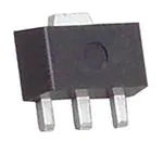
SOT-89
Figure 1.
Description
The START499D provide the market with a Si
state-of-art RF process. Manufactured with ST 3rd
generation bipolar process, it offers the highest
power, gain and efficiency in SOT-89 for given
breakdown voltage (BVCEo). START499D is
suitable for a wide range of application up to 1
GHz.
)
s
(
ct
r
P
e
Pin connection
t
e
l
o
bs
Emitter
O
)
s
(
t
c
u
d
o
e
t
e
ol
Pr
Base
Emitter
Collector
s
b
O
Table 1.
Device summary
Order code
Marking
Package
Packaging
START499D
D499
SOT-89
Tape and reel
June 2010
Doc ID 14496 Rev 4
1/18
www.st.com
18
�Contents
START499D
Contents
1
2
Electrical data . . . . . . . . . . . . . . . . . . . . . . . . . . . . . . . . . . . . . . . . . . . . . . 3
1.1
Maximum ratings . . . . . . . . . . . . . . . . . . . . . . . . . . . . . . . . . . . . . . . . . . . . 3
1.2
Thermal data . . . . . . . . . . . . . . . . . . . . . . . . . . . . . . . . . . . . . . . . . . . . . . . 3
Electrical characteristics . . . . . . . . . . . . . . . . . . . . . . . . . . . . . . . . . . . . . 4
2.1
Static . . . . . . . . . . . . . . . . . . . . . . . . . . . . . . . . . . . . . . . . . . . . . . . . . . . . . 4
2.2
Dynamic . . . . . . . . . . . . . . . . . . . . . . . . . . . . . . . . . . . . . . . . . . . . . . . . . . . 4
)
s
(
ct
u
d
o
3
Impedance . . . . . . . . . . . . . . . . . . . . . . . . . . . . . . . . . . . . . . . . . . . . . . . . . 5
4
Typical performance . . . . . . . . . . . . . . . . . . . . . . . . . . . . . . . . . . . . . . . . . 6
5
Test circuit, part list and photo . . . . . . . . . . . . . . . . . . . . . . . . . . . . . . . 10
6
Package mechanical data . . . . . . . . . . . . . . . . . . . . . . . . . . . . . . . . . . . . 12
r
P
e
t
e
l
o
s
b
O
6.1
Thermal pad and via design . . . . . . . . . . . . . . . . . . . . . . . . . . . . . . . . . . . 14
6.2
Soldering profile . . . . . . . . . . . . . . . . . . . . . . . . . . . . . . . . . . . . . . . . . . . . 15
)
(s
t
c
u
7
Revision history . . . . . . . . . . . . . . . . . . . . . . . . . . . . . . . . . . . . . . . . . . . 17
d
o
r
P
e
t
e
l
o
s
b
O
2/18
Doc ID 14496 Rev 4
�START499D
Electrical data
1
Electrical data
1.1
Maximum ratings
Table 2.
Absolute maximum ratings (TCASE = +25 °C)
Symbol
Value
Unit
VCEO
Collector - emitter voltage
4.5
V
VEBO
Emitter - base voltage
1.5
V
Collectorcurrent
1.0
A
Power dissipation
1.7
Max. operating junction temperature
150
IC
PDISS
TJ
TSTG
1.2
Parameter
r
P
e
Thermal data
Symbol
)
(s
t
e
l
o
s
b
O
Parameter
Junction - case thermal resistance
RthJC
uc
-65 to +150
Thermal data
Table 3.
W
od
Storage temperature
)
s
(
t
°C
°C
Value
Unit
75
°C/W
t
c
u
d
o
r
P
e
t
e
l
o
s
b
O
Doc ID 14496 Rev 4
3/18
�Electrical characteristics
START499D
2
Electrical characteristics
2.1
Static
Table 4.
Static TCASE = +25 oC
Symbol
Min.
Max.
Unit
VCB = 15 V
5
µA
IEBO
VEB = 1.2 V
250
µA
BVCES
IC = 200 µA
VCE = 3 V
15
20
IC = 0.16 A
)
s
(
ct
u
d
o
r
P
e
Dynamic
Symbol
Test conditions
t
e
l
o
POUT
GP
V
150
Dynamic
Table 5.
s
b
O
VCC = 3.6 V, ICQ = 30 mA, PIN = 15 dBm, f = 900 MHz
hD
Load
VCC = 3.6 V, ICQ = 30 mA, POUT = 28 dBm, f = 900 MHz
mismatch All phase angles
)-
s
(
t
c
u
d
o
r
P
e
t
e
l
o
s
b
O
4/18
Typ.
ICBO
hFE
2.2
Test conditions
Doc ID 14496 Rev 4
Min.
Typ.
28
29
dBm
13
14
dB
55
65
%
3:1
Max.
Unit
VSWR
�START499D
3
Impedance
Impedance
Figure 2.
Current conventions
ZL
C
ZS
B
)
s
(
ct
E
Table 6.
u
d
o
Frequency (MHz)
ZBS (Ω)
800
16.58 - j4.04
820
15.81 - j3.81
16.28 - j5.11
840
bs
15.04 - j3.53
14.77 - j4.67
14.31 - j3.21
13.44 - j4.15
13.61 - j2.83
12.25 - j3.54
12.93 - j2.44
11.19 - j2.90
12.27 - j2.01
10.24 - j2.22
940
11.66 - j1.53
9.40 - j1.52
960
11.06 - j1.04
8.65 - j0.81
980
10.52 - j0.54
7.99 - j0.11
1000
9.98 + j0.02
7.38 + j0.62
t
e
l
o
O
)
860
t(s
880
900
c
u
d
920
ro
P
e
let
o
s
b
r
P
e
Impedance data
ZCL(Ω)
17.95 - j5.49
O
Doc ID 14496 Rev 4
5/18
�Typical performance
START499D
4
Typical performance
Figure 3.
DC output characterisitics
Figure 4.
BVEBO
)
s
(
ct
START499D
START499D
u
d
o
r
P
e
Figure 5.
t
e
l
o
BVCES
)
(s
s
b
O
t
c
u
d
o
r
P
e
START499D
t
e
l
o
s
b
O
6/18
Doc ID 14496 Rev 4
�START499D
Figure 6.
Typical performance
Gain vs frequency
Figure 7.
20
Efficiency vs frequency
80
75
18
Pin=13dBm
Pin=14dBm
Pin=15dBm
Pin=13dBm
Pin=14dBm
Pin=15dBm
Efficiency [%]
70
Gain[dB]
16
14
65
)
s
(
ct
60
Vcc = 3.6V
Icq = 30mA
12
55
u
d
o
Vcc = 3.6V
Icq = 30mA
10
800
820
840
860
880
900
920
940
960
980
50
800 820 840 860 880 900 920 940 960 980 1000
1000
r
P
e
Frequency [MHz]
Frequency [MHz]
Gain and efficiency vs frequency
y
q
17
100
16
90
t(s
c
u
d
Gain [dB]
14
12
e
t
e
l
11
o
s
b
10
800
O
)-
820
840
860
o
r
P
900
70
60
Frequency [MHz]
-20
-30
-40
40
920
Vcc = 3.6V
Icq = 30mA
Pout = 28dBm
50
Vcc = 3.6V
Icq = 30mA
Pout = 28dBm
880
-10
80
Efficiency [%]
15
Harmonics vs frequency
s
b
O
0
Gain
Efficiency
13
t
e
l
o
Figure 9.
y
Harmonics [dBc]
Figure 8.
940
960
980
30
1000
-50
H_2nd
H_3rd
-60
800
820
840
860
880
900
920
940
960
980 1000
Frequency [MHz]
Doc ID 14496 Rev 4
7/18
�Typical performance
START499D
Figure 10. Input return loss vs frequency
Figure 11. Gain vs output power
0
20
-2
Vcc = 3.6V
Icq = 30mA
Pout = 28dBm
-4
18
860MHz
910MHz
960MHz
16
IRL [dB]
Gain [dB]
-6
-8
)
s
(
ct
12
-10
Vcc = 3.6V
Icq = 30mA
10
-12
-14
800
14
820
840
860
880
900
920
940
960
980
8
1000
22
Frequency [MHz]
23
24
u
d
o
Pr
25
26
27
28
29
30
Output Power [dBm]
e
t
e
ol
Figure 12. Efficiency vs output power
Figure 13. Gain vs output power
70
)-
65
50
45
ete
40
c
u
d
30
b
O
16
o
r
P
15
14
l
o
s
35
Vcc = 3 V
Icq = 30mA
17
Gain [dB]
Efficiency [%]
55
18
t(s
860MHz
910MHz
960MHz
60
s
b
O
Vcc = 3.6V
Icq = 30mA
860MHz
910MHz
960MHz
13
25
8/18
22
23
24
25
26
27
Output Pow er [dBm]
28
29
30
12
21
22
23
24
25
Output Pow er [dBm]
Doc ID 14496 Rev 4
26
27
28
�START499D
Typical performance
Figure 14. Efficiency vs output power
Figure 15. Gain vs output power
70
18
65
860MHz
910MHz
960MHz
60
910MHz
960MHz
55
16
50
Gain [dB]
Efficiency [%]
860MHz
17
45
40
Vcc = 2 V
Icq = 30mA
13
u
d
o
30
25
21
22
23
24
25
26
27
28
12
16
17
18
19
Output Pow er [dBm]
e
t
e
ol
70
)
(s
65
60
Efficiency [%]
21
22
23
24
s
b
O
t
c
u
55
d
o
r
50
P
e
45
t
e
l
o
40
35
s
b
O
30
Pr
20
Output Pow er [dBm]
Figure 16. Efficiency vs output power
860MHz
910MHz
960MHz
)
s
(
ct
14
Vcc = 3 V
Icq = 30mA
35
15
Vcc = 2 V
Icq = 30mA
25
16
17
18
19
20
21
22
23
24
Output Pow er [dBm]
Doc ID 14496 Rev 4
9/18
�Test circuit, part list and photo
5
START499D
Test circuit, part list and photo
Figure 17. Test circuit schematic
18 m A
C1 1
FR4
Er = 4 .5
H = 2 0 mil
C6
C7
V cc
3. 6 V
C8
R3
B1
R2
BJT2
B C8 4 7
L2
C9
C1 0
)
s
(
ct
L3
C 12
R1
C5
u
d
o
L1
TL 4
RF _ in
T L1
T L2
r
P
e
TL 5
TL 3
C1
BJT1
C2
S TA RT4 9 9D
C4
TL 6
RF_ o ut
C3
t
e
l
o
Table 7.
Components part list
Component ID
Description
C1,C3,C5,C9
Capacitor
C2
Capacitor
C4
Capacitor
C6,C10,C11
Case size
Manufacturer
Part code
100 pF
1608
Murata
GRM1885C1H101JA01
5.6 pF
1608
Murata
GRM1885C1HR50CZ01
6.8 pF
1608
Murata
GRM1885C1H6R8CZ01
Capacitor
1 nF
1608
Murata
GRM1885C1H102JA01
C7
Capacitor
10 nF
1608
Murata
GRM188R71H103KA01
C8
Capacitor
1 uF
1608
Murata
GRM188R71H105KA01
L1
Inductor
11 nH
1608
Coilcraft
0603CS-11NXGB
L2
Inductor
100 nH
1608
Coilcraft
0603CS-R10XGB
L3
Inductor
5.4 nH
2012
Coilcraft
0906-5JLB
B1
Ferrite bead
Panasonic
EXCELDRC35C
R1
Resister
30 ohm
1608
R3
Resister
180 ohm
1608
R2
Potentiometer
10 KΩ
s
b
O
t
c
u
od
e
t
e
ol
10/18
)
(s
Value
s
b
O
Pr
1608 chip resister
(0.063 W, ±5 %)
Bourns electronics
TL1
Transmission line L=11.9 mm W=0.9 mm
TL2
Transmission line
L=5.0 mm
W=0.9 mm
TL3
Transmission line
L=5.2 mm
W=0.9 mm
Doc ID 14496 Rev 4
3214W-1-103E
�START499D
Table 7.
Test circuit, part list and photo
Components part list (continued)
Component ID
Description
Value
Case size
TL4
Transmission line
L=3.5 mm
W=0.9 mm
TL5
Transmission line
L=2.8 mm
W=0.9 mm
TL6
Transmission line L=12.2 mm W=0.9 mm
Manufacturer
Part code
BJT2
BJT
STMicroelectronics
BC847
BJT1
BJT
STMicroelectronics
START499D
Board
FR4 Er=4.5 THk=0.020" 1OZ Cu both sides
)
s
(
ct
Figure 18. Photo
u
d
o
r
P
e
t
e
l
o
)
(s
s
b
O
t
c
u
d
o
r
P
e
t
e
l
o
s
b
O
Doc ID 14496 Rev 4
11/18
�Package mechanical data
6
START499D
Package mechanical data
In order to meet environmental requirements, ST offers these devices in different grades of
ECOPACK® packages, depending on their level of environmental compliance. ECOPACK®
specifications, grade definitions and product status are available at: www.st.com.
ECOPACK is an ST trademark.
)
s
(
ct
u
d
o
r
P
e
t
e
l
o
)
(s
s
b
O
t
c
u
d
o
r
P
e
t
e
l
o
s
b
O
12/18
Doc ID 14496 Rev 4
�START499D
Package mechanical data
Table 8.
SOT-89 mechanical data
Dim.
mm.
Min
Typ
Inch
Max
Min
Typ
Max
A
1.4
1.6
55.1
63.0
B
0.44
0.56
17.3
22.0
B1
0.36
0.48
14.2
18.9
C
0.35
0.44
13.8
17.3
C1
0.35
0.44
13.8
17.3
D
4.4
4.6
173.2
181.1
D1
1.62
1.83
63.8
E
2.40
2.6
94.5
e
1.42
1.57
55.9
e1
2.92
3.07
115.0
H
3.94
4.25
155.1
L
0.89
1.2
e
t
e
l
35.0
)
s
(
ct
72.0
Pr
u
d
o
102.4
61.8
120.9
167.3
47.2
o
s
b
Figure 19. Package dimensions
O
)
s
(
t
c
u
d
o
r
P
e
t
e
l
o
s
b
O
Doc ID 14496 Rev 4
13/18
�Package mechanical data
6.1
START499D
Thermal pad and via design
Thernal vias are required in the PCB layout to effectively conduct heat away from the
package. The via pattern has been designed to address thermal, power dissipation and
electrical requirements of the device.
The via pattern is based on thru-hole vias with 0.203 mm to 0.330 mm finished hole size on
a 0.5 mm to 1.2 mm grid pattern with 0.025 plating on via walls. If micro vias are used in a
design, it is suggested that the quantity of vias be increased by a 4:1 ratio to achieve similar
results.
Figure 20. Pad layout details
)
s
(
ct
u
d
o
r
P
e
t
e
l
o
)
(s
t
c
u
s
b
O
SOT-89
d
o
r
P
e
t
e
l
o
s
b
O
14/18
Doc ID 14496 Rev 4
�START499D
6.2
Package mechanical data
Soldering profile
Figure 21 shows the recommeded solder for devices that have Pb-free terminal plating and
where a Pb-free solder is used.
Figure 21. Recommended solder profile
)
s
(
ct
u
d
o
r
P
e
t
e
l
o
s
b
O
Figure 22 shows the recommeded solder for devices with Pb-free terminal plating used with
leaded solder, or for devices with leaded terminal plating used with a leaded solder.
)
(s
Figure 22. Recommended solder profile for leaded devices
t
c
u
d
o
r
P
e
t
e
l
o
s
b
O
Doc ID 14496 Rev 4
15/18
�Package mechanical data
START499D
Figure 23. Reel information
)
s
(
ct
u
d
o
r
P
e
t
e
l
o
)
(s
s
b
O
t
c
u
d
o
r
P
e
t
e
l
o
s
b
O
16/18
Doc ID 14496 Rev 4
�START499D
7
Revision history
Revision history
Table 9.
Document revision history
Date
Revision
Changes
03-Mar-2008
1
Initial release.
15-Jul-2008
2
Updated Table 1 on page 1.
17-Jul-2008
3
Values update on Table 4 on page 4.
29-Jun-2010
4
Updated Table 8 on page 13.
)
s
(
ct
u
d
o
r
P
e
t
e
l
o
)
(s
s
b
O
t
c
u
d
o
r
P
e
t
e
l
o
s
b
O
Doc ID 14496 Rev 4
17/18
�START499D
)
s
(
ct
Please Read Carefully:
u
d
o
Information in this document is provided solely in connection with ST products. STMicroelectronics NV and its subsidiaries (“ST”) reserve the
right to make changes, corrections, modifications or improvements, to this document, and the products and services described herein at any
time, without notice.
r
P
e
All ST products are sold pursuant to ST’s terms and conditions of sale.
Purchasers are solely responsible for the choice, selection and use of the ST products and services described herein, and ST assumes no
liability whatsoever relating to the choice, selection or use of the ST products and services described herein.
t
e
l
o
No license, express or implied, by estoppel or otherwise, to any intellectual property rights is granted under this document. If any part of this
document refers to any third party products or services it shall not be deemed a license grant by ST for the use of such third party products
or services, or any intellectual property contained therein or considered as a warranty covering the use in any manner whatsoever of such
third party products or services or any intellectual property contained therein.
)
(s
s
b
O
UNLESS OTHERWISE SET FORTH IN ST’S TERMS AND CONDITIONS OF SALE ST DISCLAIMS ANY EXPRESS OR IMPLIED
WARRANTY WITH RESPECT TO THE USE AND/OR SALE OF ST PRODUCTS INCLUDING WITHOUT LIMITATION IMPLIED
WARRANTIES OF MERCHANTABILITY, FITNESS FOR A PARTICULAR PURPOSE (AND THEIR EQUIVALENTS UNDER THE LAWS
OF ANY JURISDICTION), OR INFRINGEMENT OF ANY PATENT, COPYRIGHT OR OTHER INTELLECTUAL PROPERTY RIGHT.
t
c
u
UNLESS EXPRESSLY APPROVED IN WRITING BY AN AUTHORIZED ST REPRESENTATIVE, ST PRODUCTS ARE NOT
RECOMMENDED, AUTHORIZED OR WARRANTED FOR USE IN MILITARY, AIR CRAFT, SPACE, LIFE SAVING, OR LIFE SUSTAINING
APPLICATIONS, NOR IN PRODUCTS OR SYSTEMS WHERE FAILURE OR MALFUNCTION MAY RESULT IN PERSONAL INJURY,
DEATH, OR SEVERE PROPERTY OR ENVIRONMENTAL DAMAGE. ST PRODUCTS WHICH ARE NOT SPECIFIED AS "AUTOMOTIVE
GRADE" MAY ONLY BE USED IN AUTOMOTIVE APPLICATIONS AT USER’S OWN RISK.
d
o
r
P
e
t
e
l
o
Resale of ST products with provisions different from the statements and/or technical features set forth in this document shall immediately void
any warranty granted by ST for the ST product or service described herein and shall not create or extend in any manner whatsoever, any
liability of ST.
s
b
O
ST and the ST logo are trademarks or registered trademarks of ST in various countries.
Information in this document supersedes and replaces all information previously supplied.
The ST logo is a registered trademark of STMicroelectronics. All other names are the property of their respective owners.
© 2010 STMicroelectronics - All rights reserved
STMicroelectronics group of companies
Australia - Belgium - Brazil - Canada - China - Czech Republic - Finland - France - Germany - Hong Kong - India - Israel - Italy - Japan Malaysia - Malta - Morocco - Philippines - Singapore - Spain - Sweden - Switzerland - United Kingdom - United States of America
www.st.com
18/18
Doc ID 14496 Rev 4
�