物料型号:STB37N60DM2AG
器件简介:
- 该MOSFET属于MDmesh™ DM2快速恢复二极管系列,具有非常低的恢复电荷(Qrr)和时间(trr),结合低RDS(on),适合要求高效率转换器,非常适合桥式拓扑和ZVS相移转换器。
引脚分配:
- D(2,TAB):漏极
- G(1):栅极
- S(3):源极
参数特性:
- 600V电压等级
- 典型导通电阻(RDS(on))为0.110Ω
- 28A连续漏极电流
- 210W总功耗
功能详解:
- 专为汽车应用设计并通过AEC-Q101认证
- 快速恢复体二极管
- 极低的栅极电荷和输入电容
- 100%雪崩测试
- 极高的dv/dt坚固性
- Zener保护
应用信息:
- 开关应用
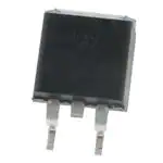
封装信息:
- D2PAK封装
- 胶带和卷轴包装
电气特性:
- 包括静态特性、动态特性、开关时间、源-漏二极管特性和栅-源Zener二极管特性等详细参数。
测试电路:
- 提供了用于电阻负载开关时间、栅极电荷行为、感性负载开关和二极管恢复时间、无钳位感性负载测试电路等的测试电路图。
封装信息:
- 提供了D²PAK (TO-263)类型A封装的机械数据和推荐足迹。
修订历史:
- 文档的初始版本发布于2015年8月25日。
重要声明:
- STMicroelectronics NV及其子公司保留随时更改、更正、增强、修改和改进ST产品和/或本文档的权利。