STB60NH02L
N-CHANNEL 24V - 0.0085 Ω - 60A D²PAK
STripFET™ III POWER MOSFET
TYPE
STB60NH02L
■
■
■
■
■
■
■
VDSS
RDS(on)
ID
24 V
< 0.0105 Ω
60 A
TYPICAL RDS(on) = 0.0085 Ω @ 10 V
TYPICAL RDS(on) = 0.012 Ω @ 5 V
RDS(ON) * Qg INDUSTRY’s BENCHMARK
CONDUCTION LOSSES REDUCED
SWITCHING LOSSES REDUCED
LOW THRESHOLD DEVICE
SURFACE-MOUNTING D2PAK (TO-263)
POWER PACKAGE IN TUBE (NO SUFFIX) OR
IN TAPE & REEL (SUFFIX “T4”)
DESCRIPTION
The STB60NH02L utilizes the latest advanced design
rules of ST’s proprietary STripFET™ technology. This is
suitable fot the most demanding DC-DC converter
application where high efficiency is to be achieved.
)
(s
)
s
(
ct
u
d
o
3
1
r
P
e
D2PAK
TO-263
(Suffix “T4”)
t
e
l
o
s
b
O
INTERNAL SCHEMATIC DIAGRAM
APPLICATIONS
■ SPECIFICALLY DESIGNED AND OPTIMISED
FOR HIGH EFFICIENCY DC/DC CONVERTES
t
c
u
d
o
r
P
e
t
e
l
o
Ordering Information
SALES TYPE
STB60NH02LT4
s
b
O
MARKING
B60NH02L
PACKAGE
TO-263
PACKAGING
TAPE & REEL
ABSOLUTE MAXIMUM RATINGS
Symbol
Vspike(1)
VDS
VDGR
VGS
ID
ID
IDM(2)
Ptot
EAS (3)
Tstg
Tj
May 2004
Parameter
Drain-source Voltage Rating
Drain-source Voltage (VGS = 0)
Drain-gate Voltage (RGS = 20 kΩ)
Gate- source Voltage
Drain Current (continuous) at TC = 25°C
Drain Current (continuous) at TC = 100°C
Drain Current (pulsed)
Total Dissipation at TC = 25°C
Derating Factor
Single Pulse Avalanche Energy
Storage Temperature
Max. Operating Junction Temperature
Value
30
24
24
± 20
60
43
240
70
0.47
280
Unit
V
V
V
V
A
A
A
W
W/°C
mJ
-55 to 175
°C
1/11
�STB60NH02L
THERMAL DATA
Rthj-case
Rthj-amb
Tl
Max
Max
Thermal Resistance Junction-case
Thermal Resistance Junction-ambient
Maximum Lead Temperature For Soldering Purpose
°C/W
°C/W
°C
2.14
62.5
300
ELECTRICAL CHARACTERISTICS (TCASE = 25 °C UNLESS OTHERWISE SPECIFIED)
OFF
Symbol
V(BR)DSS
IDSS
IGSS
Parameter
Test Conditions
Drain-source
Breakdown Voltage
ID = 25 mA, VGS = 0
Zero Gate Voltage
Drain Current (VGS = 0)
VDS = 20 V
VDS = 20 V
Gate-body Leakage
Current (VDS = 0)
VGS = ± 20V
Min.
Parameter
Gate Threshold Voltage
VDS = VGS
ID = 250 µA
RDS(on)
Static Drain-source On
Resistance
VGS = 10 V
VGS = 5 V
ID = 30 A
ID = 15 A
Symbol
gfs (4)
Forward Transconductance
Ciss
Coss
Crss
Input Capacitance
Output Capacitance
Reverse Transfer
Capacitance
RG
2/11
o
r
P
Gate Input Resistance
s
b
O
Test Conditions
t(s
c
u
d
e
t
e
ol
s
b
O
)-
Parameter
VDS = 15 V
1
10
µA
µA
±100
nA
)
s
(
ct
ID = 25 A
VDS = 15V f = 1 MHz VGS = 0
f = 1 MHz Gate DC Bias = 0
Test Signal Level = 20 mV
Open Drain
1
u
d
o
Pr
Min.
e
t
e
ol
VGS(th)
Unit
V
TC = 125°C
Test Conditions
DYNAMIC
Max.
24
ON (4)
Symbol
Typ.
Min.
Typ.
Max.
Unit
1.8
2.5
V
0.0085
0.012
0.0105
0.020
Ω
Ω
Typ.
Max.
Unit
27
S
1400
400
55
pF
pF
pF
1
Ω
�STB60NH02L
ELECTRICAL CHARACTERISTICS (continued)
SWITCHING ON
Symbol
Parameter
Test Conditions
Min.
Typ.
td(on)
tr
Turn-on Delay Time
Rise Time
VDD = 10 V
ID = 30 A
VGS = 10 V
RG = 4.7 Ω
(Resistive Load, Figure 3)
10
130
Qg
Qgs
Qgd
Total Gate Charge
Gate-Source Charge
Gate-Drain Charge
VDD= 10 V ID= 60 A VGS= 10 V
24
5
3.4
Output Charge
VDS= 16 V
9.4
Qoss(5)
VGS= 0 V
Max.
ns
ns
32
td(off)
tf
Parameter
Test Conditions
VDD = 10 V
ID = 30 A
VGS = 10 V
RG = 4.7Ω,
(Resistive Load, Figure 3)
Turn-off Delay Time
Fall Time
)
s
(
ct
Symbol
Parameter
ISD
ISDM
Source-drain Current
Source-drain Current (pulsed)
trr
Qrr
IRRM
Reverse Recovery Time
Reverse Recovery Charge
Reverse Recovery Current
c
u
d
.
.
e
t
e
ol
Safe Operating Area
t(s
o
r
P
Min.
Max.
Unit
27
16
21.6
ns
ns
Typ.
Max.
Unit
60
240
A
A
1.3
V
48
48
ns
nC
A
bs
O
)
ISD = 30 A
Forward On Voltage
(1) Garanted when external Rg=4.7 Ω and tf < tfmax.
(2) Pulse width limited by safe operating area
(3) Starting Tj = 25 oC, ID = 25A, VDD = 15V
s
b
O
Test Conditions
Typ.
u
d
o
r
P
e
t
e
l
o
SOURCE DRAIN DIODE
VSD (4)
Min.
VGS = 0
ISD = 60 A
di/dt = 100A/µs
Tj = 150°C
VDD = 18 V
(see test circuit, Figure 5)
nC
nC
nC
nC
SWITCHING OFF
Symbol
Unit
36
36
2
(4) Pulsed: Pulse duration = 300 µs, duty cycle 1.5 %.
(5) Qoss = Coss*∆ Vin , Coss = Cgd + Cds . See Appendix A
Thermal Impedance
3/11
�STB60NH02L
Output Characteristics
Transfer Characteristics
)
s
(
ct
u
d
o
r
P
e
Transconductance
Static Drain-source On Resistance
t
e
l
o
)
(s
s
b
O
t
c
u
d
o
r
P
e
t
e
l
o
Gate Charge vs Gate-source Voltage
s
b
O
4/11
Capacitance Variations
�STB60NH02L
Normalized Gate Threshold Voltage vs Temperature
Normalized on Resistance vs Temperature
)
s
(
ct
u
d
o
r
P
e
Source-drain Diode Forward Characteristics
Normalized Breakdown Voltage vs Temperature
t
e
l
o
)
(s
s
b
O
t
c
u
d
o
r
P
e
.
s
b
O
t
e
l
o
.
5/11
�STB60NH02L
Fig. 1: Unclamped Inductive Load Test Circuit
Fig. 2: Unclamped Inductive Waveform
)
s
(
ct
Fig. 3: Switching Times Test Circuits For Resistive
Load
)
(s
t
c
u
d
o
r
P
e
t
e
l
o
Fig. 5: Test Circuit For Inductive Load Switching
And Diode Recovery Times
s
b
O
6/11
u
d
o
r
P
e
Fig. 4: Gate Charge test Circuit
s
b
O
t
e
l
o
�STB60NH02L
D2PAK MECHANICAL DATA
mm.
DIM.
MIN.
TYP.
inch.
MAX.
MIN.
TYP.
TYP.
A
4.4
4.6
0.173
0.181
A1
2.49
2.69
0.098
0.106
A2
0.03
0.23
0.001
0.009
B
0.7
0.93
0.028
0.037
B2
1.14
1.7
0.045
0.067
C
0.45
0.6
0.018
0.024
C2
1.21
1.36
0.048
D
8.95
9.35
0.352
10.4
0.394
D1
0.368
8
E
E1
r
P
e
8.5
G
4.88
5.28
L
15
15.85
1.27
1.4
L3
1.4
1.75
M
2.4
3.2
R
0.192
s
(
t
c
4°
0.208
0.050
t
e
l
o
0.055
0.055
0.069
0.094
0.126
0.591
bs
O
)
0.4
0°
0.409
0.334
L2
V2
u
d
o
0.315
10
)
s
(
ct
0.054
0.624
0.015
0°
4°
u
d
o
r
P
e
t
e
l
o
s
b
O
7/11
�STB60NH02L
D2PAK FOOTPRINT
TUBE SHIPMENT (no suffix)*
)
s
(
ct
u
d
TAPE AND REEL SHIPMENT (suffix ”T4”)*
o
r
P
e
t
e
l
o
s
b
O
)
s
(
t
c
u
d
o
r
P
e
REEL MECHANICAL DATA
DIM.
mm
MIN.
A
B
t
e
l
o
DIM.
bs
MAX.
MIN.
MAX.
10.5
10.7
0.413
0.421
B0
15.7
15.9
0.618
0.626
D
1.5
1.6
0.059
0.063
D1
1.59
1.61
0.062
0.063
E
1.65
1.85
0.065
0.073
F
11.4
11.6
0.449
0.456
K0
4.8
5.0
0.189
0.197
0.161
P0
3.9
4.1
0.153
P1
11.9
12.1
0.468
0.476
P2
1.9
2.1
0075
0.082
R
50
T
0.25
0.35
.0.0098
0.0137
W
23.7
24.3
0.933
0.956
* on sales type
8/11
inch
MIN.
A0
O
mm
1.574
inch
MIN.
330
1.5
C
12.8
D
20.2
G
24.4
N
100
T
TAPE MECHANICAL DATA
MAX.
MAX.
12.992
0.059
13.2
0.504
0.520
0.795
26.4
0.960
1.039
3.937
30.4
1.197
BASE QTY
BULK QTY
1000
1000
�STB60NH02L
)
s
(
ct
u
d
o
r
P
e
t
e
l
o
)
(s
s
b
O
t
c
u
d
o
r
P
e
t
e
l
o
s
b
O
9/11
�STB60NH02L
)
s
(
ct
u
d
o
r
P
e
t
e
l
o
)
(s
t
c
u
d
o
r
P
e
t
e
l
o
s
b
O
10/11
s
b
O
�STB60NH02L
)
s
(
ct
u
d
o
r
P
e
t
e
l
o
)
(s
s
b
O
t
c
u
d
o
r
P
e
t
e
l
o
s
b
O
Information furnished is believed to be accurate and reliable. However, STMicroelectronics assumes no responsibility for the consequences
of use of such information nor for any infringement of patents or other rights of third parties which may result from its use. No license is granted
by implication or otherwise under any patent or patent rights of STMicroelectronics. Specifications mentioned in this publication are subject
to change without notice. This publication supersedes and replaces all information previously supplied. STMicroelectronics products are not
authorized for use as critical components in life support devices or systems without express written approval of STMicroelectronics.
The ST logo is registered trademark of STMicroelectronics
All other names are the property of their respective owners.
© 2004 STMicroelectronics - All Rights Reserved
STMicroelectronics GROUP OF COMPANIES
Australia - Belgium - Brazil - Canada - China - Czech Republic - Finland - France - Germany - Hong Kong - India - Israel - Italy - Japan Malaysia - Malta - Morocco -Singapore - Spain - Sweden - Switzerland - United Kingdom - United States.
www.st.com
11/11
�
很抱歉,暂时无法提供与“STB60NH02LT4”相匹配的价格&库存,您可以联系我们找货
免费人工找货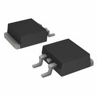


 工商网监
湘ICP备2023018690号
工商网监
湘ICP备2023018690号
