STB95N3LLH6, STD95N3LLH6
STP95N3LLH6, STU95N3LLH6
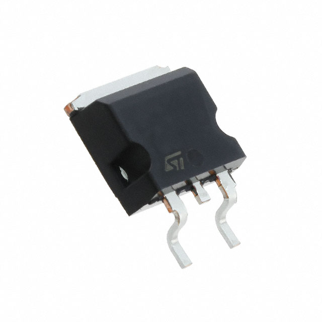
N-channel 30 V, 0.0037 Ω , 80 A, D2PAK, DPAK, IPAK, TO-220
STripFET™ VI DeepGATE™ Power MOSFET
Features
Type
VDSS
RDS(on) max
ID
30 V
0.0042 Ω
STD95N3LLH6
30 V
0.0042 Ω
80 A
STP95N3LLH6
30 V
0.0042 Ω
80 A
STU95N3LLH6
30 V
0.0047 Ω
80 A
STB95N3LLH6
■
RDS(on) * Qg industry benchmark
■
Extremely low on-resistance RDS(on)
■
High avalanche ruggedness
■
Low gate drive power losses
3
1
80 A
3
2
DPAK
1
IPAK
3
1
3
1
D²PAK
2
TO-220
Application
■
Figure 1.
Switching applications
Internal schematic diagram
D (TAB or 2)
Description
This product utilizes the 6th generation of design
rules of ST’s proprietary STripFET™ technology,
with a new gate structure.The resulting Power
MOSFET exhibits the lowest RDS(on) in all
packages.
G(1)
S(3)
AM01474v1
Table 1.
Device summary
Order codes
Marking
Package
Packaging
STB95N3LLH6
95N3LLH6
D²PAK
Tape and reel
STD95N3LLH6
95N3LLH6
DPAK
Tape and reel
STP95N3LLH6
95N3LLH6
TO-220
Tube
STU95N3LLH6
95N3LLH6
IPAK
Tube
November 2009
Doc ID 15228 Rev 3
1/18
www.st.com
18
�Contents
STx95N3LLH6
Contents
1
Electrical ratings . . . . . . . . . . . . . . . . . . . . . . . . . . . . . . . . . . . . . . . . . . . . 3
2
Electrical characteristics . . . . . . . . . . . . . . . . . . . . . . . . . . . . . . . . . . . . . 4
2.1
Electrical characteristics (curves)
.............................. 6
3
Test circuits
4
Package mechanical data . . . . . . . . . . . . . . . . . . . . . . . . . . . . . . . . . . . . 10
5
Packaging mechanical data . . . . . . . . . . . . . . . . . . . . . . . . . . . . . . . . . . 16
6
Revision history . . . . . . . . . . . . . . . . . . . . . . . . . . . . . . . . . . . . . . . . . . . 18
2/18
.............................................. 8
Doc ID 15228 Rev 3
�STx95N3LLH6
1
Electrical ratings
Electrical ratings
Table 2.
Absolute maximum ratings
Symbol
Parameter
Value
Unit
30
V
± 20
V
Drain current (continuous) at TC = 25 °C
80
A
Drain current (continuous) at TC = 100 °C
61
A
Drain current (pulsed)
320
A
Total dissipation at TC = 25 °C
70
W
Derating factor
0.47
W/°C
Single pulse avalanche energy
150
mJ
-55 to 175
°C
175
°C
VDS
Drain-source voltage (VGS = 0)
VGS
Gate-source voltage
ID
(1)
ID
IDM
(2)
PTOT
EAS (3)
Tstg
Tj
Storage temperature
Max. operating junction temperature
1. Limited by wire bonding
2. Pulse width limited by safe operating area
3. Starting Tj = 25°C, IAV = 55 A, L = 0.1 mH
Table 3.
Thermal data
Value
Symbol
Parameter
Unit
D²PAK
Rthj-case
Thermal resistance junction-case
max
Rthj-amb
Thermal resistance junction-ambient
max
Rthj-pcb(1)
Tl
Thermal resistance junction-pcb
max
DPAK
IPAK
TO-220
2.14
100
35
Maximum lead temperature for
soldering purpose
°C/W
62.5
35
275
°C/W
°C/W
300
°C
1. When mounted on FR-4 board of 1 inch2, 2 oz Cu.
Doc ID 15228 Rev 3
3/18
�Electrical characteristics
2
STx95N3LLH6
Electrical characteristics
(TCASE = 25 °C unless otherwise specified)
Table 4.
Symbol
Parameter
Test conditions
Drain-source breakdown
Voltage
ID = 250 µA, VGS= 0
IDSS
Zero gate voltage drain
current (VGS = 0)
VDS = 30 V
VDS = 30 V,Tc = 125 °C
IGSS
Gate body leakage current
(VDS = 0)
VGS = ± 20 V
Gate threshold voltage
VDS = VGS, ID = 250 µA
V(BR)DSS
VGS(th)
RDS(on)
Table 5.
Symbol
Static drain-source on
resistance
Min.
Typ.
1
1
10
µA
µA
±100
nA
2.5
V
VGS = 10 V, ID = 40 A
SMD version
0.0037 0.0042
Ω
VGS = 10 V, ID = 40 A
0.0042 0.0047
Ω
VGS = 4.5 V, ID = 40 A
SMD version
0.0055
0.007
Ω
VGS = 4.5 V, ID = 40 A
0.006
0.0075
Ω
Min
Typ.
Max.
Unit
-
pF
pF
pF
-
nC
nC
nC
Dynamic
Ciss
Coss
Crss
Input capacitance
Output capacitance
Reverse transfer
capacitance
VDS = 25 V, f=1 MHz,
VGS = 0
-
2200
400
280
Qg
Qgs
Qgd
Total gate charge
Gate-source charge
Gate-drain charge
VDD = 15 V, ID = 80 A
VGS = 4.5 V
Figure 13
-
20
8.2
7.5
Pre Vth gate-to-source
charge
Post Vth gate-to-source
charge
VDD = 15 V, ID = 80 A
Figure 18
-
Gate input resistance
f = 1 MHz gate bias
Bias = 0 test signal
level = 20 mV
open drain
-
RG
Unit
V
Test conditions
Qgs2
Max.
30
Parameter
Qgs1
4/18
Static
Doc ID 15228 Rev 3
3.4
nC
-
6.2
1
nC
-
Ω
�STx95N3LLH6
Electrical characteristics
Table 6.
Symbol
Switching on/off (inductive load)
Parameter
Test conditions
Min.
Typ.
Max.
Unit
td(on)
tr
Turn-on delay time
Rise time
VDD = 15 V, ID = 40 A,
RG = 4.7 Ω, VGS = 5 V
Figure 12
-
19
91
-
ns
ns
td(off)
tf
Turn-off delay time
Fall time
VDD = 15 V, ID = 40 A,
RG = 4.7 Ω, VGS = 5 V
Figure 12
-
24.5
23.4
-
ns
ns
Min.
Typ.
Max.
Unit
-
80
320
A
A
1.1
V
Table 7.
Symbol
ISD
ISDM
(1)
VSD(2)
trr
Qrr
IRRM
Source drain diode
Parameter
Test conditions
Source-drain current
Source-drain current (pulsed)
Forward on voltage
ISD = 40 A, VGS = 0
-
Reverse recovery time
Reverse recovery charge
Reverse recovery current
ISD = 80 A,
di/dt = 100 A/µs,
VDD = 24 V
Figure 14
-
28.6
22.8
1.6
ns
nC
A
1. Pulse width limited by safe operating area
2. Pulsed: pulse duration = 300 µs, duty cycle 1.5%
Doc ID 15228 Rev 3
5/18
�Electrical characteristics
STx95N3LLH6
2.1
Electrical characteristics (curves)
Figure 2.
Safe operating area
Figure 3.
Thermal impedance
AM03376v1
ID
(A)
280dpc
K
δ=0.5
s
ai
re n)
s a DS(o
R
n i max
tio
ra by
e
d
Op ite
Lim
hi
nt
100
0.2
0.1
100µs
10
0.05
-1
10
0.02
1ms
Tj=175°C
Tc=25°C
1
Sinlge
pulse
tp
Single pulse
-2
0.1
0.1
10
1
Figure 4.
VDS(V)
Output characteristics
VGS=10V
7V
300
10 -5
10
-4
τ
-2
-3
10
Figure 5.
AM03379v1
ID
(A)
Zth=k Rthj-c
δ=tp/τ
0.01
10ms
-1
10
10
tp (s)
10
Transfer characteristics
ID
(A)
AM03380v1
VDS=2V
300
6V
250
250
200
200
5V
150
150
4V
100
100
50
50
3V
0
0
Figure 6.
2
4
Normalized BVDSS vs temperature
AM03381v1
BVDSS
(norm)
0
0
VDS(V)
Figure 7.
2
4
6
8
Static drain source on resistance
AM03382v1
RDS(on)
(mΩ)
@250µA
VGS(V)
7
VGS=10V
6
1.05
5
1.00
4
3
2
0.95
1
0.90
-55 -30
6/18
-5 20 45 70
95 120 145 TJ(°C)
Doc ID 15228 Rev 3
0
0
10
20
30
40
ID(A)
�STx95N3LLH6
Figure 8.
Electrical characteristics
Gate charge vs gate-source voltage Figure 9.
AM03378v1
VGS
(V)
VDD=15V
12
Capacitance variations
AM03377v1
C
(pF)
ID=80A
10
Ciss
8
1000
6
Coss
4
Crss
2
100
0
0
10
20
30
40
Figure 10. Normalized gate threshold voltage
vs temperature
VGS(th)
(norm)
5
50 Qg(nC)
AM03383v1
@250µA
20
20 VDS(V)
AM03384v1
RDS(on)
(norm)
1.8
1.0
1.6
0.8
1.4
0.6
1.2
0.4
1.0
0.2
0.8
20 45 70 95 120 145 TJ(°C)
15
Figure 11. Normalized on resistance vs
temperature
1.2
0
-55 -30 -5
10
VGS=10V
ID=40A
0.6
-55 -30 -5 20 45 70 95 120 145 TJ(°C)
Doc ID 15228 Rev 3
7/18
�Test circuits
3
STx95N3LLH6
Test circuits
Figure 12. Switching times test circuit for
resistive load
Figure 13. Gate charge test circuit
VDD
12V
47kΩ
1kΩ
100nF
3.3
µF
2200
RL
µF
VGS
IG=CONST
VDD
100Ω
Vi=20V=VGMAX
VD
RG
2200
µF
D.U.T.
D.U.T.
VG
2.7kΩ
PW
47kΩ
1kΩ
PW
AM01468v1
AM01469v1
Figure 14. Test circuit for inductive load
Figure 15. Unclamped inductive load test
switching and diode recovery times
circuit
A
A
D.U.T.
FAST
DIODE
B
B
L
A
D
G
VD
L=100µH
S
3.3
µF
B
25 Ω
1000
µF
D
VDD
2200
µF
3.3
µF
VDD
ID
G
RG
S
Vi
D.U.T.
Pw
AM01470v1
Figure 16. Unclamped inductive waveform
AM01471v1
Figure 17. Switching time waveform
ton
V(BR)DSS
tdon
VD
toff
tr
tdoff
tf
90%
90%
IDM
10%
ID
VDD
10%
0
VDD
VDS
90%
VGS
AM01472v1
8/18
0
Doc ID 15228 Rev 3
10%
AM01473v1
�STx95N3LLH6
Test circuits
Figure 18. Gate charge waveform
Id
Vds
Vgs
Vgs(th)
Qgs1 Qgs2
Qgd
Doc ID 15228 Rev 3
9/18
�Package mechanical data
4
STx95N3LLH6
Package mechanical data
In order to meet environmental requirements, ST offers these devices in different grades of
ECOPACK® packages, depending on their level of environmental compliance. ECOPACK®
specifications, grade definitions and product status are available at: www.st.com.
ECOPACK is an ST trademark.
10/18
Doc ID 15228 Rev 3
�STx95N3LLH6
Package mechanical data
TO-251 (IPAK) mechanical data
mm.
DIM.
min.
typ
max.
A
2.20
2.40
A1
0.90
1.10
b
0.64
0.90
b2
0.95
b4
5.20
5.40
c
0.45
0.60
c2
0.48
0.60
D
6.00
6.20
E
6.40
6.60
e
e1
2.28
4.40
4.60
H
16.10
L
9.00
9.40
(L1)
0.80
1.20
L2
0.80
V1
10 o
0068771_H
Doc ID 15228 Rev 3
11/18
�Package mechanical data
STx95N3LLH6
TO-252 (DPAK) mechanical data
DIM.
mm.
min.
typ
max.
A
2.20
2.40
A1
0.90
1.10
A2
0.03
0.23
b
0.64
0.90
b4
5.20
5.40
c
0.45
0.60
c2
0.48
0.60
D
6.00
6.20
D1
E
5.10
6.40
6.60
E1
4.70
e
2.28
e1
4.40
4.60
H
9.35
10.10
L
1
L1
2.80
L2
L4
0.80
0.60
1
R
V2
0.20
8o
0o
0068772_G
12/18
Doc ID 15228 Rev 3
�STx95N3LLH6
Package mechanical data
D²PAK (TO-263) mechanical data
mm
inch
Dim
Min
A
A1
b
b2
c
c2
D
D1
E
E1
e
e1
H
J1
L
L1
L2
R
V2
Typ
4.40
0.03
0.70
1.14
0.45
1.23
8.95
7.50
10
8.50
Max
Min
4.60
0.23
0.93
1.70
0.60
1.36
9.35
0.173
0.001
0.027
0.045
0.017
0.048
0.352
0.295
0.394
0.334
10.40
2.54
4.88
15
2.49
2.29
1.27
1.30
Max
0.181
0.009
0.037
0.067
0.024
0.053
0.368
0.409
0.1
5.28
15.85
2.69
2.79
1.40
1.75
0.192
0.590
0.099
0.090
0.05
0.051
8°
0°
0.4
0°
Typ
0.208
0.624
0.106
0.110
0.055
0.069
0.016
8°
0079457_M
Doc ID 15228 Rev 3
13/18
�Package mechanical data
STx95N3LLH6
TO-220 type A mechanical data
mm
Dim
Min
A
b
b1
c
D
D1
E
e
e1
F
H1
J1
L
L1
L20
L30
∅P
Q
Typ
4.40
0.61
1.14
0.48
15.25
Max
4.60
0.88
1.70
0.70
15.75
1.27
10
2.40
4.95
1.23
6.20
2.40
13
3.50
10.40
2.70
5.15
1.32
6.60
2.72
14
3.93
16.40
28.90
3.75
2.65
3.85
2.95
0015988_Rev_S
14/18
Doc ID 15228 Rev 3
�STx95N3LLH6
5
Packaging mechanical data
Packaging mechanical data
DPAK FOOTPRINT
All dimensions are in millimeters
TAPE AND REEL SHIPMENT
REEL MECHANICAL DATA
DIM.
mm
MIN.
A
B
1.5
C
12.8
D
20.2
G
16.4
N
50
T
TAPE MECHANICAL DATA
DIM.
mm
inch
MIN.
MAX.
A0
6.8
7
0.267 0.275
B0
10.4
10.6
0.409 0.417
B1
D
1.5
D1
1.5
E
1.65
MIN.
12.1
0.476
1.6
0.059 0.063
1.85
0.065 0.073
7.4
7.6
0.291 0.299
2.55
2.75
0.100 0.108
0.153 0.161
P0
3.9
4.1
P1
7.9
8.1
0.311 0.319
P2
1.9
2.1
0.075 0.082
40
15.7
MAX.
330
12.992
13.2
0.504 0.520
18.4
0.645 0.724
0.059
0.795
1.968
22.4
0.881
BASE QTY
BULK QTY
2500
2500
0.059
F
R
MIN.
MAX.
K0
W
inch
MAX.
1.574
16.3
0.618
0.641
Doc ID 15228 Rev 3
15/18
�Packaging mechanical data
STx95N3LLH6
D 2 PAK FOOTPRINT
TAPE AND REEL SHIPMENT
REEL MECHANICAL DATA
DIM.
mm
MIN.
A
B
DIM.
16/18
mm
inch
MIN.
MAX.
MIN.
A0
10.5
10.7
0.413 0.421
MAX.
B0
15.7
15.9
0.618 0.626
0.059 0.063
D
1.5
1.6
D1
1.59
1.61
0.062 0.063
E
1.65
1.85
0.065 0.073
0.449 0.456
F
11.4
11.6
K0
4.8
5.0
0.189 0.197
P0
3.9
4.1
0.153 0.161
P1
11.9
12.1
0.468 0.476
P2
1.9
2.1
0.075 0.082
R
50
1.574
T
0.25
0.35 0.0098 0.0137
W
23.7
24.3
0.933 0.956
Doc ID 15228 Rev 3
MIN.
330
1.5
C
12.8
D
20.2
G
24.4
N
100
T
TAPE MECHANICAL DATA
inch
MAX.
MAX.
12.992
0.059
13.2
0.504 0.520
26.4
0.960 1.039
0795
3.937
30.4
1.197
BASE QTY
BULK QTY
1000
1000
�STx95N3LLH6
6
Revision history
Revision history
Table 8.
Document revision history
Date
Revision
Changes
01-Dec-2008
1
First release
20-May-2009
2
– Document status promoted from preliminary data to datasheet.
– Added new package, mechanical data: D²PAK
10-Nov-2009
3
Added new device in TO-220
Doc ID 15228 Rev 3
17/18
�STx95N3LLH6
Please Read Carefully:
Information in this document is provided solely in connection with ST products. STMicroelectronics NV and its subsidiaries (“ST”) reserve the
right to make changes, corrections, modifications or improvements, to this document, and the products and services described herein at any
time, without notice.
All ST products are sold pursuant to ST’s terms and conditions of sale.
Purchasers are solely responsible for the choice, selection and use of the ST products and services described herein, and ST assumes no
liability whatsoever relating to the choice, selection or use of the ST products and services described herein.
No license, express or implied, by estoppel or otherwise, to any intellectual property rights is granted under this document. If any part of this
document refers to any third party products or services it shall not be deemed a license grant by ST for the use of such third party products
or services, or any intellectual property contained therein or considered as a warranty covering the use in any manner whatsoever of such
third party products or services or any intellectual property contained therein.
UNLESS OTHERWISE SET FORTH IN ST’S TERMS AND CONDITIONS OF SALE ST DISCLAIMS ANY EXPRESS OR IMPLIED
WARRANTY WITH RESPECT TO THE USE AND/OR SALE OF ST PRODUCTS INCLUDING WITHOUT LIMITATION IMPLIED
WARRANTIES OF MERCHANTABILITY, FITNESS FOR A PARTICULAR PURPOSE (AND THEIR EQUIVALENTS UNDER THE LAWS
OF ANY JURISDICTION), OR INFRINGEMENT OF ANY PATENT, COPYRIGHT OR OTHER INTELLECTUAL PROPERTY RIGHT.
UNLESS EXPRESSLY APPROVED IN WRITING BY AN AUTHORIZED ST REPRESENTATIVE, ST PRODUCTS ARE NOT
RECOMMENDED, AUTHORIZED OR WARRANTED FOR USE IN MILITARY, AIR CRAFT, SPACE, LIFE SAVING, OR LIFE SUSTAINING
APPLICATIONS, NOR IN PRODUCTS OR SYSTEMS WHERE FAILURE OR MALFUNCTION MAY RESULT IN PERSONAL INJURY,
DEATH, OR SEVERE PROPERTY OR ENVIRONMENTAL DAMAGE. ST PRODUCTS WHICH ARE NOT SPECIFIED AS "AUTOMOTIVE
GRADE" MAY ONLY BE USED IN AUTOMOTIVE APPLICATIONS AT USER’S OWN RISK.
Resale of ST products with provisions different from the statements and/or technical features set forth in this document shall immediately void
any warranty granted by ST for the ST product or service described herein and shall not create or extend in any manner whatsoever, any
liability of ST.
ST and the ST logo are trademarks or registered trademarks of ST in various countries.
Information in this document supersedes and replaces all information previously supplied.
The ST logo is a registered trademark of STMicroelectronics. All other names are the property of their respective owners.
© 2009 STMicroelectronics - All rights reserved
STMicroelectronics group of companies
Australia - Belgium - Brazil - Canada - China - Czech Republic - Finland - France - Germany - Hong Kong - India - Israel - Italy - Japan Malaysia - Malta - Morocco - Philippines - Singapore - Spain - Sweden - Switzerland - United Kingdom - United States of America
www.st.com
18/18
Doc ID 15228 Rev 3
�