STBR3012
Datasheet
High voltage rectifier for bridge applications
Features
A1
K
K
•
•
•
•
Ultra low conduction losses
Ultra-low reverse losses
High junction temperature capability (+175 °C)
D²PAK HV creepage distance (anode to cathode) = 5.38 mm min. (with top
coating)
•
ECOPACK®2 compliant (DO-247)
A
A
A
K
DO-247
NC
D²PAK HV
Applications
•
•
SMPS
Bridge
Description
The high quality design of this diode has produced a device with consistently
reproducible characteristics and intrinsic ruggedness. These characteristics make it
ideal for heavy duty applications that demand long term reliability like automotive
applications.
Thanks to its ultra-low conduction losses, the STBR3012 is especially suitable for
use as input bridge diode in battery chargers.
Product status link
STBR3012
Product summary
Symbol
Value
IF(AV)
30 A
VRRM
1200 V
Tj
+175 °C
VF (typ.)
0.95 V
DS11909 - Rev 2 - November 2018
For further information contact your local STMicroelectronics sales office.
www.st.com
�STBR3012
Characteristics
1
Characteristics
Table 1. Absolute ratings (limiting values at 25 °C, unless otherwise specified)
Symbol
Parameter
Value
Unit
VRSM
Non-repetitive surge reverse voltage
1500
V
VRRM
Repetitive peak reverse voltage
1200
V
IF(RMS)
Forward rms current
45
A
IF(AV)
Average forward current
TC = 155 °C, δ = 0.5 square wave
30
A
IFSM
Surge non repetitive forward current
tp = 10 ms sinusoidal
300
A
Tstg
Storage temperature range
-65 to +175
°C
+175
°C
Tj
Operating junction temperature
Table 2. Thermal parameters
Symbol
Rth(j-c)
Parameter
Typ. value
Unit
0.45
°C/W
Junction to case
For more information, please refer to the following application note:
•
AN5088: Rectifiers thermal management, handling and mounting recommendations
Table 3. Static electrical characteristics
Symbol
Parameter
IR(1)
Reverse leakage current
VF(2)
Forward voltage drop
Test conditions
Tj = 25 °C
Tj = 150 °C
Tj = 25 °C
Tj = 150 °C
VR = VRRM
IF = 30 A
Min.
Typ.
-
Max.
2
-
10
100
-
1.05
1.3
-
0.95
1.2
Unit
µA
V
1. Pulse test: tp = 5 ms, δ < 2%
2. Pulse test: tp = 380 µs, δ < 2%
To evaluate the conduction losses, use the following equation:
P = 0.96 x IF(AV) + 0.008 x IF2(RMS)
For more information, please refer to the following application notes related to the power losses:
•
AN604: Calculation of conduction losses in a power rectifier
•
AN4021: Calculation of reverse losses in a power diode
DS11909 - Rev 2
page 2/12
�STBR3012
Characteristics (curves)
1.1
Characteristics (curves)
Figure 1. Average forward power dissipation versus
average forward current
Figure 2. Forward voltage drop versus forward current
(typical values)
P(W)
50
1,0E+03
δ = 0.5
40
IFM(A)
δ= 1
1,0E+02
δ = 0.2
Tj = 150 °C
δ = 0.1
30
1,0E+01
δ = 0.05
20
Tj = 25 °C
1,0E+00
T
1,0E-01
10
tp
δ =tp/T
IF(AV)(A)
VFM(V)
0
0
5
10
15
20
25
30
35
Figure 3. Forward voltage drop versus forward current
(maximum values)
1,0E+03
1,0E-02
0,0
1,0
1,5
2,0
Figure 4. Relative variation of thermal impedance junction
to case versus pulse duration
IFM(A)
1,0
0,9
1,0E+02
0,5
Zth(j-c) /Rth(j-c)
Single pulse
0,8
Tj = 150 °C
0,7
Tj = 25 °C
1,0E+01
0,6
0,5
0,4
1,0E+00
0,3
0,2
1,0E-01
0,1
VFM(V)
0,0
1,E-03
1,0E-02
0,0
DS11909 - Rev 2
0,5
1,0
1,5
2,0
t P(s)
1,E-02
1,E-01
1,E+00
2,5
page 3/12
�STBR3012
Characteristics (curves)
Figure 5. Junction capacitance versus reverse voltage
applied (typical values)
1000
Figure 6. Relative variation of non-repetitive peak surge
forward current versus pulse duration (sinusoidal
waveform)
C(pF)
IFSM(t p ) / IFSM(10ms)
4.0
F = 1 MHz
Vosc = 30 mVRMS
Tj = 25 °C
3.5
3.0
100
2.5
2.0
VR(V)
1.5
10
1
10
100
1000
10000
t p (ms)
1.0
0.1
Figure 7. Relative variation of non-repetitive peak surge
forward current versus initial junction temperature
(sinusoidal waveform)
1.2
1.0
10.0
Figure 8. Thermal resistance junction to ambient versus
copper surface under tab (typical values, epoxy printed
board FR4, eCu = 35µm) (D²PAK HV)
IFSM(T j) / IFSM(25°C)
80
Rth(j-a) (°C/W)
70
1.0
60
0.8
50
40
0.6
30
0.4
20
0.2
10
T j(°C)
0.0
25
DS11909 - Rev 2
50
75
100
125
150
175
SCu (cm²)
0
0
5
10
15
20
25
30
35
40
page 4/12
�STBR3012
Package information
2
Package information
In order to meet environmental requirements, ST offers these devices in different grades of ECOPACK®
packages, depending on their level of environmental compliance. ECOPACK® specifications, grade definitions
and product status are available at: www.st.com. ECOPACK® is an ST trademark.
2.1
DO-247 package information
•
•
•
•
Epoxy meets UL94, V0
Cooling method: by conduction (C)
Recommended torque value: 0.8 N·m (DO-247)
Maximum torque value: 1.0 N·m (DO-247)
Figure 9. DO-247 package outline
V
Dia
V
A
H
0.10
L5
L
L2
L4
F2
L1
F3
L3
D
V2
F
G
DS11909 - Rev 2
M
E
page 5/12
�STBR3012
DO-247 package information
Table 4. DO-247 package mechanical data
Dimensions
Ref.
Millimeters
Min.
Max.
Min.
Max.
A
4.85
5.15
0.191
0.203
D
2.20
2.60
0.086
0.102
E
0.40
0.80
0.015
0.031
F
1.00
1.40
0.039
0.055
F2
F3
2.00 typ.
2.00
G
0.078 typ.
2.40
0.078
10.90 typ.
0.094
0.429 typ.
H
15.45
15.75
0.608
0.620
L
19.85
20.15
0.781
0.793
L1
3.70
4.30
0.145
0.169
L2
L3
18.50 typ.
14.20
0.728 typ.
14.80
0.559
0.582
L4
34.60 typ.
1.362 typ.
L5
5.50 typ.
0.216 typ.
M
2.00
3.00
0.078
0.118
V
5°
5°
V2
60°
60°
Dia.
DS11909 - Rev 2
Inches
3.55
3.65
0.139
0.143
page 6/12
�STBR3012
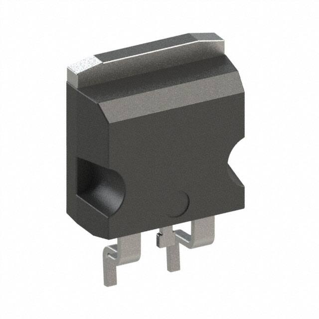
D²PAK high voltage package information
2.2
D²PAK high voltage package information
Figure 10. D²PAK high voltage package outline
A
H
C
L1
L
R
L4
R
M
L2
0.25 gauge plane
F (x2)
E
e
H1
L3
A1
V
DS11909 - Rev 2
page 7/12
�STBR3012
D²PAK high voltage package information
Table 5. D²PAK high voltage package mechanical data
Ref.
Dimensions
Min.
Typ.
Max.
A
4.30
4.70
A1
0.03
0.20
C
1.17
1.37
e
4.98
5.18
E
0.50
0.90
F
0.78
0.85
H
10.00
10.40
H1
7.40
7.80
L
15.30
15.80
L1
1.27
1.40
L2
4.93
5.23
L3
6.85
7.25
L4
1.5
1.7
M
2.6
2.9
R
0.20
0.60
V
0°
8°
Figure 11. D²PAK High Voltage footprint in mm
10,58
7,46
15,95
5,10
3,40
1,20
5,08
DS11909 - Rev 2
page 8/12
�STBR3012
D²PAK high voltage package information
2.2.1
Creepage distance between anode and cathode
Table 6. Creepage distance between anode and cathode
Symbol
Note:
Parameter
CdA-K1
Minimum creepage distance between A and K1 (with top coating)
CdA-K2
Minimum creepage distance between A and K2 (without top coating)
Value
D²PAK HV
5.38
3.48
Unit
mm
D²PAK HV creepage distance (anode to cathode) = 5.38 mm min. (refer to IEC 60664-1)
Figure 12. Creepage with top coating
Figure 13. Creepage without top coating
DS11909 - Rev 2
page 9/12
�STBR3012
Ordering information
3
Ordering information
Table 7. Ordering information
DS11909 - Rev 2
Order code
Marking
Package
Weight
Base qty.
Delivery mode
STBR3012W
STBR3012W
DO-247
4.4 g
30
Tube
STBR3012G2-TR
STBR3012G2
D²PAK HV
1.48 g
1000
Tape and reel
page 10/12
�STBR3012
Revision history
Table 8. Document revision history
DS11909 - Rev 2
Date
Revision
Changes
02-Nov-2016
1
First issue.
19-Nov-2018
2
Added D²PAK HV.
page 11/12
�STBR3012
IMPORTANT NOTICE – PLEASE READ CAREFULLY
STMicroelectronics NV and its subsidiaries (“ST”) reserve the right to make changes, corrections, enhancements, modifications, and improvements to ST
products and/or to this document at any time without notice. Purchasers should obtain the latest relevant information on ST products before placing orders. ST
products are sold pursuant to ST’s terms and conditions of sale in place at the time of order acknowledgement.
Purchasers are solely responsible for the choice, selection, and use of ST products and ST assumes no liability for application assistance or the design of
Purchasers’ products.
No license, express or implied, to any intellectual property right is granted by ST herein.
Resale of ST products with provisions different from the information set forth herein shall void any warranty granted by ST for such product.
ST and the ST logo are trademarks of ST. All other product or service names are the property of their respective owners.
Information in this document supersedes and replaces information previously supplied in any prior versions of this document.
© 2018 STMicroelectronics – All rights reserved
DS11909 - Rev 2
page 12/12
�