STCL1100 STCL1120 STCL1160
High frequency silicon oscillator family
Not recommended for new design
Features
■
Fixed frequency 10/12/16 MHz
■
±1.5% frequency accuracy over all conditions
■
5 V ±10% operation
■
Low operating current, ultra low standby
current
■
Push-pull, CMOS compatible frequency
(square wave) output
■
Chip enable input, active high
■
Fast and stable startup
■
No external components required
■
Temperature range: –20 to +85 °C,
0 to +105 °C
■
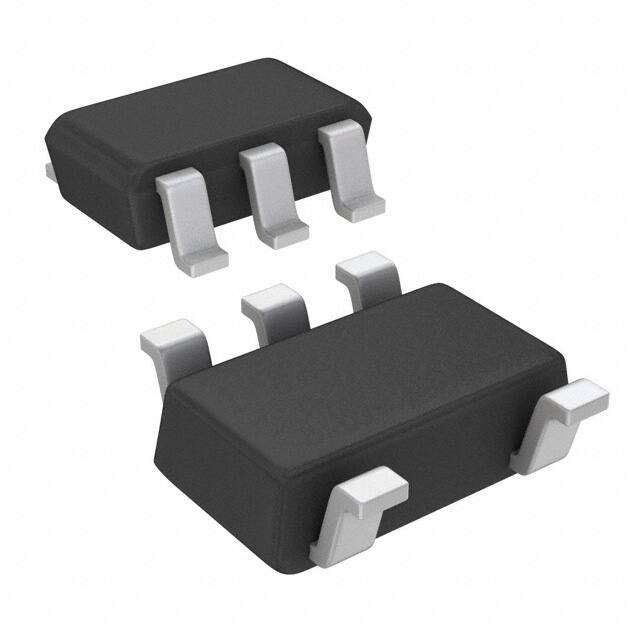
Package: SOT23-5L
■
RoHS compliant.
SOT23-5L
Applications
■
Motor control
■
Home appliances
■
Building control
■
Advanced battery chargers
■
Low speed USB applications
■
Display drivers
■
Generally where ceramic resonators are
currently being used.
June 2010
Doc ID 13337 Rev 4
This is information on a product still in production but not recommended for new designs.
1/18
www.st.com
1
�Contents
STCL1100 STCL1120 STCL1160
Contents
1
Description . . . . . . . . . . . . . . . . . . . . . . . . . . . . . . . . . . . . . . . . . . . . . . . . . 5
2
Pin connections . . . . . . . . . . . . . . . . . . . . . . . . . . . . . . . . . . . . . . . . . . . . . 6
2.1
Signal names . . . . . . . . . . . . . . . . . . . . . . . . . . . . . . . . . . . . . . . . . . . . . . . 6
3
Typical application circuit . . . . . . . . . . . . . . . . . . . . . . . . . . . . . . . . . . . . 7
4
Operation . . . . . . . . . . . . . . . . . . . . . . . . . . . . . . . . . . . . . . . . . . . . . . . . . . 8
4.1
Chip Enable (CE) . . . . . . . . . . . . . . . . . . . . . . . . . . . . . . . . . . . . . . . . . . . . 8
4.2
Transition to disable . . . . . . . . . . . . . . . . . . . . . . . . . . . . . . . . . . . . . . . . . . 8
4.3
Fast startup and wakeup from disable . . . . . . . . . . . . . . . . . . . . . . . . . . . . 8
5
Maximum rating . . . . . . . . . . . . . . . . . . . . . . . . . . . . . . . . . . . . . . . . . . . . . 9
6
DC and AC parameters . . . . . . . . . . . . . . . . . . . . . . . . . . . . . . . . . . . . . . 10
7
Typical operating characteristics and scope plots . . . . . . . . . . . . . . . 12
8
Package details SOT23-5L . . . . . . . . . . . . . . . . . . . . . . . . . . . . . . . . . . . 15
9
Part numbering . . . . . . . . . . . . . . . . . . . . . . . . . . . . . . . . . . . . . . . . . . . . 16
10
Revision history . . . . . . . . . . . . . . . . . . . . . . . . . . . . . . . . . . . . . . . . . . . 17
2/18
Doc ID 13337 Rev 4
�STCL1100 STCL1120 STCL1160
List of tables
List of tables
Table 1.
Table 2.
Table 3.
Table 4.
Table 5.
Table 6.
Absolute maximum ratings . . . . . . . . . . . . . . . . . . . . . . . . . . . . . . . . . . . . . . . . . . . . . . . . . . 9
DC and AC measurement conditions . . . . . . . . . . . . . . . . . . . . . . . . . . . . . . . . . . . . . . . . . 10
DC and AC parameters . . . . . . . . . . . . . . . . . . . . . . . . . . . . . . . . . . . . . . . . . . . . . . . . . . . 11
SOT23-5L - 5-lead small outline transistor package mechanical data . . . . . . . . . . . . . . . . 15
Ordering information scheme . . . . . . . . . . . . . . . . . . . . . . . . . . . . . . . . . . . . . . . . . . . . . . . 16
Document revision history . . . . . . . . . . . . . . . . . . . . . . . . . . . . . . . . . . . . . . . . . . . . . . . . . 17
Doc ID 13337 Rev 4
3/18
�List of figures
STCL1100 STCL1120 STCL1160
List of figures
Figure 1.
Figure 2.
Figure 3.
Figure 4.
Figure 5.
Figure 6.
Figure 7.
Figure 8.
Figure 9.
4/18
SOT23-5L . . . . . . . . . . . . . . . . . . . . . . . . . . . . . . . . . . . . . . . . . . . . . . . . . . . . . . . . . . . . . . . 6
Microprocessor (MCU, microcontroller unit) clock example
- replacement of a crystal or ceramic resonator . . . . . . . . . . . . . . . . . . . . . . . . . . . . . . . . . . 7
Frequency vs. temperature, STCL1120 . . . . . . . . . . . . . . . . . . . . . . . . . . . . . . . . . . . . . . . 12
Duty cycle vs. temperature, STCL1120 . . . . . . . . . . . . . . . . . . . . . . . . . . . . . . . . . . . . . . . 12
Active supply current vs. temperature, STCL1120 . . . . . . . . . . . . . . . . . . . . . . . . . . . . . . . 13
Standby supply current vs. temperature, STCL1120 . . . . . . . . . . . . . . . . . . . . . . . . . . . . . 13
Startup time vs. temperature, STCL1120 . . . . . . . . . . . . . . . . . . . . . . . . . . . . . . . . . . . . . . 14
Startup output waveform, first cycles zoom (power-on), STCL1120. . . . . . . . . . . . . . . . . . 14
SOT23-5L - 5-lead small outline transistor package outline . . . . . . . . . . . . . . . . . . . . . . . . 15
Doc ID 13337 Rev 4
�STCL1100 STCL1120 STCL1160
1
Description
Description
The STCL1100, STCL1120 and STCL1160 silicon oscillator devices are reliable, easy to
use, 5-pin low-cost fixed frequency silicon oscillators developed primarily for microprocessor
clock applications, display drivers or other system applications where tighter clock accuracy
is not critical. Compared to ceramic resonators and crystal oscillators, silicon oscillators
offer the advantages of faster startup, smaller size and improved immunity to shock,
vibration and EMI.
The STCL1100, STCL1120 and STCL1160 silicon oscillator devices are equipped with chip
enable input, offering an easy way to stop microprocessor clocking during a power saving
mode while at the same time significantly reducing the oscillator current consumption.
Doc ID 13337 Rev 4
5/18
�Pin connections
2
STCL1100 STCL1120 STCL1160
Pin connections
Figure 1.
SOT23-5L
CE
1
NC
2
FOUT
3
5
VCC
4
GND
AI12656
2.1
Signal names
VCC
Positive supply voltage pin
FOUT Frequency (square wave) output, CMOS compatible, push-pull
CE
Chip Enable input, active high, no internal pull-up resistor
GND Ground
NC
6/18
No Connect
Doc ID 13337 Rev 4
�STCL1100 STCL1120 STCL1160
Typical application circuit
3
Typical application circuit
Figure 2.
Microprocessor (MCU, microcontroller unit) clock example
- replacement of a crystal or ceramic resonator
MCU
CE (2)
I/O
NC
2
VCC
5V
5
0.1 µF(1)
STCL1xx0
FOUT
Xtal1
(OSC1,
OSCin)
Xtal2
(OSC2,
OSCout)
VCC
1
GND
3
4
GND
NC
AI12657d
1. For reliable operation and to further improve immunity to harsh environment, the minimum 0.1 µF decoupling capacitor is
recommended to be placed as close as possible to the VCC and GND pins of the oscillator device. The whole oscillator
block should then be placed near the microprocessor clock input.
2. To minimize standby current, no internal pull-up resistor to VCC is implemented on the CE input, thus the input level must
be permanently defined by the controlling signal. If the chip enable feature is not used, in active mode connect the CE pin
to VCC. In applications utilizing standby mode and where the CE pin is connected to the controlling I/O port of the clocked
microprocessor, for successful startup of the microprocessor at power-on, initial logic high level needs to be secured on the
CE pin to provide clock already during the power-on reset until the microprocessor program starts and the controlling I/O
port takes over the CE control.
Doc ID 13337 Rev 4
7/18
�Operation
4
STCL1100 STCL1120 STCL1160
Operation
Use of the STCL1xx0 silicon oscillator device is very simple. Once power is applied to VCC
pin, a CMOS-compatible square wave output signal is provided on the FOUT output pin (in
active mode the Chip Enable (CE) input pin must be at a logic high level).
4.1
Chip Enable (CE)
This feature allows the user to stop the clock and significantly reduce the current
consumption when the application is put into power saving mode.
When used to clock the microprocessor in place of a crystal, the need for chip enable input
stems from a difference in the way microprocessors normally disable their clock. In the case
of a crystal or ceramic resonator, when going into power saving mode, the processor simply
opens the internal Xtal inverter feedback which results in stopping the crystal oscillations;
however in the case of the silicon oscillators this would not work and the oscillator would
continue to run. So in order to use this feature, one of the microprocessor's output pins must
be configured to control the silicon oscillator's Chip Enable (CE) input, see Typical
application circuit diagram. To minimize standby current of the oscillator device, no internal
pull-up resistor is implemented on the CE input, thus the input level must be permanently
defined by the controlling signal.
4.2
Transition to disable
The device provides additional 32 complete clock cycles after the chip enable input went
inactive to allow the clocked microprocessor to complete pipelined instructions before going
into sleep mode. Then during disable the output remains low.
4.3
Fast startup and wakeup from disable
The total startup time until oscillations internally stabilize and remain within specifications is
50 µs max from the point when VCC reached min operating voltage (at power on) or from the
point when CE went active (wakeup from disable mode). The output remains low even
during initial 16 cycles after CE went active to provide stabilized valid output waveform
already from the first output cycle, see Table 3: DC and AC parameters and Figure 8:
Startup output waveform, first cycles zoom (power-on), STCL1120. Compare to
milliseconds typical for crystal oscillators or hundreds of microseconds for ceramic
resonators.
8/18
Doc ID 13337 Rev 4
�STCL1100 STCL1120 STCL1160
5
Maximum rating
Maximum rating
Stressing the device above the rating listed in the Table 1: Absolute maximum ratings may
cause permanent damage to the device. These are stress ratings only and operation of the
device at these or any other conditions above those indicated in the Operating sections of
this specification is not implied. Exposure to absolute maximum rating conditions for
extended periods may affect device reliability. Refer also to the STMicroelectronics SURE
Program and other relevant quality documents.
Table 1.
Symbol
TSTG
TSLD
Absolute maximum ratings
Parameter
Note
Storage temperature (VCC Off)
Lead solder temperature for 10
seconds
VIO
Input or output voltage
VCC
Supply voltage
Lead-free lead
finish(1)
Value
Unit
–55 to 150
°C
260
°C
–0.3 to VCC +0.3
V
–0.3 to 7
V
1. Reflow at peak temperature of 260 °C (total thermal budget not to exceed 245 °C for more than 30 seconds).
Doc ID 13337 Rev 4
9/18
�DC and AC parameters
6
STCL1100 STCL1120 STCL1160
DC and AC parameters
This section summarizes the operating and measurement conditions, as well as the DC and
AC characteristics of the device. The parameters in the following Table 3: DC and AC
parameters are derived from tests performed under the DC and AC measurement
conditions listed in the Table 2. Designers should check that the operating conditions in their
projects match the measurement conditions when using the quoted parameters.
Table 2.
DC and AC measurement conditions(1)
Parameter
VCC supply voltage
4.5 to 5.5 V
Ambient operating temperature
–20 to +85 °C
Load capacitance (CL)
12 pF
1. Unless other specified.
10/18
Doc ID 13337 Rev 4
�STCL1100 STCL1120 STCL1160
Table 3.
Sym
DC and AC parameters
DC and AC parameters(1)
Description
VCC
Operating voltage
ICC
Operating current
Test condition
Min
Typ
Max
Unit
4.5
5.0
5.5
V
FOUT = 10 MHz, output unloaded
590
800
µA
FOUT = 10 MHz, output
unloaded, 0 to +105 °C
(STCL1100YBFCWY7)
590
900
µA
FOUT = 12 MHz, output unloaded
650
900
µA
FOUT = 16 MHz, output unloaded
800
1050
µA
2
3
µA
0.4
V
ICC2
Standby current
CE = 0 V
VOL
Output voltage low
IOL = 3 mA
VOH
Output voltage high
IOH = –3 mA
VIL
Input low voltage (CE input)
VIH
Input high voltage (CE input)
2
ILI
Input leakage current (CE input)
–1
VCC –0.4 V
V
0.8
Frequency accuracy
over all conditions(2), (3)
VCC = 4.5 to 5.5 V,
–20 to +85 °C (0 to +105 °C
for STCL1100YBFCWY7)
Jitter
Period jitter, over 20 s
Duty cycle
Taken at half of the signal
amplitude
V
+1
µA
±1.5
%
±150
40
V
psP-P
50
60
%
20
µs
tSTART Startup time(4)
From the point when VCC
reached min operating voltage or
CE went active until the
oscillations stabilize within
specifications.
10
tR, tF
CL = 12 pF; 10 to 90% of the
amplitude
5
ns
12
pF
CL
Rise/fall time
Load capacitance
1. Valid for Ambient Operating Temperature: TA = –20 to +85 °C; VCC = 4.5 to 5.5 V (except where noted).
2. Frequency vs. temperature characteristics has its maximum at room temperature, for both higher and lower temperatures
the frequency decreases. Therefore, to reach symmetrical tolerances, the devices are factory-trimmed at room temperature
to the frequency value close to higher tolerance limit. See Typical operating characteristics.
3. The specified values are for the recommended configuration, i.e. parts properly soldered on PCB, with 0.1 µF ceramic
capacitor soldered close to the VCC-GND pins and short leads between the output and scope probe (to minimize signal
reflections; see output waveform screenshots for various conditions). Recommended is usage of the active scope probe
that adds around 1 pF of the load capacity to the total load and having frequency counter connected to the scope output as
input capacitance of the counter is typically in tens of pF. Installing the device in a socket may have an influence on the
frequency and repeatability as well, depending on quality of its contacts.
4. For details see startup waveform graph - Figure 8.
Doc ID 13337 Rev 4
11/18
�Typical operating characteristics and scope plots
STCL1100 STCL1120 STCL1160
7
Typical operating characteristics and scope plots
Figure 3.
Frequency vs. temperature, STCL1120
12 .100
12 .050
12 .000
Mean
frequency
(MHz)
11.950
11.900
11.850
–40
–20
0
25
70
85
125
Temperature (˚C)
4V
4.5 V
5V
5.5 V
6V
AI14581
Figure 4.
Duty cycle vs. temperature, STCL1120
45.5
45.0
44.5
44.0
Duty
cycle (%)
43.5
43.0
42.5
42.0
41.5
–40
0
25
70
85
125
Temperature (˚C)
5.5 V
AI14582
12/18
Doc ID 13337 Rev 4
�STCL1100 STCL1120 STCL1160
Figure 5.
Typical operating characteristics and scope plots
Active supply current vs. temperature, STCL1120
1000
900
800
700
Mean
ICC (µA)
600
500
400
300
200
100
0
–40
0
25
70
85
125
Temperature (˚C)
4V
4.5 V
5V
5.5 V
6V
AI14584
Figure 6.
Standby supply current vs. temperature, STCL1120
3000
2500
2000
Mean ICC
standby (nA) 1500
1000
5 00
0
–40
0
25
70
85
125
Temperature (˚C)
4V
4.5 V
5V
5.5 V
6V
AI14585
Doc ID 13337 Rev 4
13/18
�Typical operating characteristics and scope plots
Figure 7.
STCL1100 STCL1120 STCL1160
Startup time vs. temperature, STCL1120
12
10
8
Startup
time (µs)
6
4
2
0
–40
0
25
70
85
125
Temperature (˚C)
5.5 V
AI14586a
Figure 8.
14/18
Startup output waveform, first cycles zoom (power-on), STCL1120
Doc ID 13337 Rev 4
�STCL1100 STCL1120 STCL1160
Package details SOT23-5L
8
Package details SOT23-5L
Figure 9.
SOT23-5L - 5-lead small outline transistor package outline
A1
E
e
D
D1
B
A2
K
C
A
CP
L
F
SOT23-5
Table 4.
SOT23-5L - 5-lead small outline transistor package mechanical data
millimeters
inches
Symbol
A
Typ
Min
Max
Typ
Min
Max
1.200
0.900
1.450
0.0472
0.0354
0.0571
A1
0.150
0.0059
A2
1.050
0.900
1.300
0.0413
0.0354
0.0512
B
0.400
0.350
0.500
0.0157
0.0138
0.0197
C
0.150
0.090
0.200
0.0059
0.0035
0.0079
D
2.900
2.800
3.000
0.1142
0.1102
0.1181
D1
1.900
E
2.800
0.1024
0.1181
e
0.950
F
1.600
0.0591
0.0689
0
10
0.0039
0.0236
K
L
0.350
0.0748
2.600
3.000
0.1102
0.0374
1.500
1.750
0
10
0.100
0.600
Doc ID 13337 Rev 4
0.0630
0.0138
15/18
�Part numbering
STCL1100 STCL1120 STCL1160
9
Part numbering
Table 5.
Ordering information scheme
STCL
1
120
Y
B
F
C
WY
5
Device type
STCL = Silicon oscillator
Product family
1 = Single frequency, fixed
Frequency
100 = 10.0 MHz
120 = 12.0 MHz
160 = 16.0 MHz
Operating voltage
Y = 4.5 to 5.5 V
Accuracy
B = ±1.5%
Chip enable
F = Single chip enable, active high, no pull
Disable mode
C = Additional 32 cycles, output low in disable, skip
16 cycles at startup, output low during that
Package
WY = SOT23-5L
Temperature range
5 = –20 to +85 °C
7 = 0 to +105 °C
Note:
16/18
Contact local ST sales office for availability of other product options (chip enable active high
or low, with or without internal pull-up or pull-down, possibility of various disable modes,
startup procedures, output low or in high-impedance when disabled, etc.).
Doc ID 13337 Rev 4
�STCL1100 STCL1120 STCL1160
10
Revision history
Revision history
Table 6.
Document revision history
Date
Revision
Changes
26-Mar-2007
0.1
04-May-2007
1
07-Jun-2007
1.0.1
19-Feb-2008
2
Document reformatted, updated title, Features, Description, Table 2,
Table 3, Table 5, Figure 2 to Figure 8.
09-Jan-2009
3
Updated Features (added temperature range 0 to +105 °C),
Figure 2, Chapter 4.3, Table 3 (updated ICC, Frequency - added
temperature range, updated Jitter, tSTART,), Figure 7, Table 5
(modified Device type, added temperature range 7).
24-Jun-2010
4
Document reformatted, added header and footer to cover page to
indicate change in product maturity status.
Initial release.
Parameters update in Table 3.
Typing error corrected.
Doc ID 13337 Rev 4
17/18
�STCL1100 STCL1120 STCL1160
Please Read Carefully:
Information in this document is provided solely in connection with ST products. STMicroelectronics NV and its subsidiaries (“ST”) reserve the
right to make changes, corrections, modifications or improvements, to this document, and the products and services described herein at any
time, without notice.
All ST products are sold pursuant to ST’s terms and conditions of sale.
Purchasers are solely responsible for the choice, selection and use of the ST products and services described herein, and ST assumes no
liability whatsoever relating to the choice, selection or use of the ST products and services described herein.
No license, express or implied, by estoppel or otherwise, to any intellectual property rights is granted under this document. If any part of this
document refers to any third party products or services it shall not be deemed a license grant by ST for the use of such third party products
or services, or any intellectual property contained therein or considered as a warranty covering the use in any manner whatsoever of such
third party products or services or any intellectual property contained therein.
UNLESS OTHERWISE SET FORTH IN ST’S TERMS AND CONDITIONS OF SALE ST DISCLAIMS ANY EXPRESS OR IMPLIED
WARRANTY WITH RESPECT TO THE USE AND/OR SALE OF ST PRODUCTS INCLUDING WITHOUT LIMITATION IMPLIED
WARRANTIES OF MERCHANTABILITY, FITNESS FOR A PARTICULAR PURPOSE (AND THEIR EQUIVALENTS UNDER THE LAWS
OF ANY JURISDICTION), OR INFRINGEMENT OF ANY PATENT, COPYRIGHT OR OTHER INTELLECTUAL PROPERTY RIGHT.
UNLESS EXPRESSLY APPROVED IN WRITING BY AN AUTHORIZED ST REPRESENTATIVE, ST PRODUCTS ARE NOT
RECOMMENDED, AUTHORIZED OR WARRANTED FOR USE IN MILITARY, AIR CRAFT, SPACE, LIFE SAVING, OR LIFE SUSTAINING
APPLICATIONS, NOR IN PRODUCTS OR SYSTEMS WHERE FAILURE OR MALFUNCTION MAY RESULT IN PERSONAL INJURY,
DEATH, OR SEVERE PROPERTY OR ENVIRONMENTAL DAMAGE. ST PRODUCTS WHICH ARE NOT SPECIFIED AS "AUTOMOTIVE
GRADE" MAY ONLY BE USED IN AUTOMOTIVE APPLICATIONS AT USER’S OWN RISK.
Resale of ST products with provisions different from the statements and/or technical features set forth in this document shall immediately void
any warranty granted by ST for the ST product or service described herein and shall not create or extend in any manner whatsoever, any
liability of ST.
ST and the ST logo are trademarks or registered trademarks of ST in various countries.
Information in this document supersedes and replaces all information previously supplied.
The ST logo is a registered trademark of STMicroelectronics. All other names are the property of their respective owners.
© 2010 STMicroelectronics - All rights reserved
STMicroelectronics group of companies
Australia - Belgium - Brazil - Canada - China - Czech Republic - Finland - France - Germany - Hong Kong - India - Israel - Italy - Japan Malaysia - Malta - Morocco - Philippines - Singapore - Spain - Sweden - Switzerland - United Kingdom - United States of America
www.st.com
18/18
Doc ID 13337 Rev 4
�


 工商网监
湘ICP备2023018690号
工商网监
湘ICP备2023018690号
