STD30NE06L
®
N - CHANNEL 60V - 0.025 Ω - 30A TO-252
STripFET POWER MOSFET
TYPE
VDSS
R DS(on)
ID
STD30NE06L
60 V
< 0.03 Ω
30 A
■
TYPICAL RDS(on) = 0.025 Ω
EXCEPTIONAL dv/dt CAPABILITY
100% AVALANCHE TESTED
LOW GATE CHARGE 100oC
APPLICATION ORIENTED
CHARACTERIZATION
ADD SUFFIX "T4" FOR ORDERING IN TAPE
& REEL
)
s
(
t
c
u
d
o
)
r
s
(
P
t
c
e
t
u
e
d
l
o
o
r
s
P
b
e
O
t
e
l
)
o
s
(
s
t
b
c
u
O
d
o
)
r
s
P
(
t
c
e
t
u
e
l
d
o
o
r
s
P
b
O
e
t
e
l
o
s
b
O
■
■
■
■
■
3
1
DESCRIPTION
This Power MOSFET is the latest development of
STMicroelectronics unique "Single Feature
Size" strip-based process. The resulting transistor shows extremely high packing density for low
on-resistance, rugged avalanche characteristics
and less critical alignment steps therefore a remarkable manufacturing reproducibility.
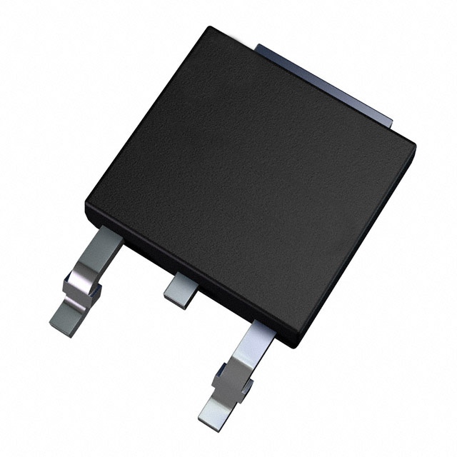
DPAK
TO-252
(Suffix "T4")
INTERNAL SCHEMATIC DIAGRAM
APPLICATIONS
HIGH CURRENT, HIGH SPEED SWITCHING
■ SOLENOID AND RELAY DRIVERS
■ MOTOR CONTROL, AUDIO AMPLIFIERS
■ DC-DC & DC-AC CONVERTERS
■
ABSOLUTE MAXIMUM RATINGS
Symbol
V DS
V DGR
VGS
Parameter
Value
Drain-source Voltage (V GS = 0)
60
V
Drain- gate Voltage (R GS = 20 kΩ)
60
V
± 20
V
30
A
Gate-source Voltage
ID
Drain Current (continuous) at T c = 25 o C
ID
o
I DM (•)
P tot
Drain Current (continuous) at T c = 100 C
21
A
Drain Current (pulsed)
120
A
Total Dissipation at T c = 25 o C
Derating Factor
dv/dt (1 ) Peak Diode Recovery voltage slope
T st g
Tj
Storage Temperature
Max. Operating Junction Temperature
(•) Pulse width limited by safe operating area
May 1999
Unit
55
W
0.37
W/ o C
7
V/ns
-65 to 175
o
C
175
o
C
(1) ISD ≤30A, di/dt ≤ 300 A/µs, VDD ≤ V(BR)DSS, Tj ≤ TJMAX
1/8
�STD30NE06L
THERMAL DATA
R thj-pcb
R thj-amb
R thj-sink
Tl
o
2.72
100
1.5
275
Thermal Resistance Junction-PC Board
Max
Thermal Resistance Junction-ambient
Max
Thermal Resistance Case-sink
Typ
Maximum Lead Temperature For Soldering Purpose
C/W
C/W
o
C/W
o
C
o
AVALANCHE CHARACTERISTICS
Symbol
IAR
Parameter
Max Value
Unit
30
A
Avalanche Current, Repetitive or Not-Repetitive
(pulse width limited by T j max)
)
s
(
t
c
u
d
o
)
r
s
(
P
t
c
e
t
u
e
d
l
o
o
r
s
P
b
e
O
t
e
l
)
o
s
(
s
t
b
c
u
O
d
o
)
r
s
P
(
t
c
e
t
u
e
l
d
o
o
r
s
P
b
O
e
t
e
l
o
s
b
O
E AS
Single Pulse Avalanche Energy
(starting T j = 25 o C, I D = I AR , V DD = 25 V)
100
mJ
ELECTRICAL CHARACTERISTICS (Tcase = 25 oC unless otherwise specified)
OFF
Symbol
V (BR)DSS
Parameter
Drain-source
Breakdown Voltage
Test Conditions
I D = 250 µA
V GS = 0
I DSS
Zero Gate Voltage
V DS = Max Rating
Drain Current (V GS = 0) V DS = Max Rating
IGSS
Gate-body Leakage
Current (V DS = 0)
Min.
Typ.
Max.
60
Unit
V
T c = 125 o C
V GS = ± 20 V
1
10
µA
µA
± 100
nA
Max.
Unit
ON (∗)
Symbol
Parameter
Test Conditions
V GS(th)
Gate Threshold Voltage V DS = V GS
R DS(on)
Static Drain-source On
Resistance
I D(on)
I D = 250 µA
V GS = 10 V
V GS = 5 V
Min.
1
I D = 15 A
I D = 15 A
On State Drain Current V DS > I D(on) x R DS(on)max
V GS = 10 V
Typ.
1.7
2.5
V
0.022
0.025
0.028
0.030
Ω
Ω
30
A
DYNAMIC
Symbol
g fs (∗)
C iss
C oss
C rss
2/8
Parameter
Test Conditions
Forward
Transconductance
V DS > I D(on) x R DS(on)max
Input Capacitance
Output Capacitance
Reverse Transfer
Capacitance
V DS = 25 V
f = 1 MHz
I D = 15 A
V GS = 0 V
Min.
Typ.
Max.
Unit
15
25
S
2370
350
90
pF
pF
pF
�STD30NE06L
ELECTRICAL CHARACTERISTICS (continued)
SWITCHING ON
Symbol
Typ.
Max.
Unit
t d(on)
tr
Turn-on Delay Time
Rise Time
Parameter
V DD = 30 V
I D = 15 A
R G = 4.7 Ω
V GS = 5 V
(Resistive Load, see fig. 3)
Test Conditions
Min.
27
100
50
135
ns
ns
Qg
Q gs
Q gd
Total Gate Charge
Gate-Source Charge
Gate-Drain Charge
V DD = 30 V I D = 30 A V GS = 5 V
31
13
13.5
41
nC
nC
nC
SWITCHING OFF
)
s
(
t
c
u
d
o
)
r
s
(
P
t
c
e
t
u
e
d
l
o
o
r
s
P
b
e
O
t
e
l
)
o
s
(
s
t
b
c
u
O
d
o
)
r
s
P
(
t
c
e
t
u
e
l
d
o
o
r
s
P
b
O
e
t
e
l
o
s
b
O
Symbol
tr(Voff)
tf
tc
Parameter
Off-voltage Rise Time
Fall Time
Cross-over Time
Test Conditions
Min.
V DD = 48 V
I D = 30 A
R G = 4.7 Ω
V GS = 5 V
(Inductive Load, see fig. 5)
Typ.
Max.
Unit
20
45
72
27
60
100
ns
ns
ns
Typ.
Max.
Unit
30
120
A
A
1.5
V
SOURCE DRAIN DIODE
Symbol
Parameter
Test Conditions
ISD
I SDM (•)
Source-drain Current
Source-drain Current
(pulsed)
V SD (∗)
Forward On Voltage
I SD = 30 A
Reverse Recovery
Time
Reverse Recovery
Charge
Reverse Recovery
Current
I SD = 30 A
di/dt = 100 A/µs
V DD = 30 V
T j = 150 o C
(see test circuit, fig. 5)
t rr
Q rr
I RRM
Min.
V GS = 0
55
ns
0.1
µC
3.5
A
(∗) Pulsed: Pulse duration = 300 µs, duty cycle 1.5 %
(•) Pulse width limited by safe operating area
Safe Operating Area
Thermal Impedance
3/8
�STD30NE06L
Output Characteristics
Transfer Characteristics
)
s
(
t
c
u
d
o
)
r
s
(
P
t
c
e
t
u
e
d
l
o
o
r
s
P
b
e
O
t
e
l
)
o
s
(
s
t
b
c
u
O
d
o
)
r
s
P
(
t
c
e
t
u
e
l
d
o
o
r
s
P
b
O
e
t
e
l
o
s
b
O
Transconductance
Static Drain-source On Resistance
Gate Charge vs Gate-source Voltage
Capacitance Variations
4/8
�STD30NE06L
Normalized Gate Threshold Voltage vs
Temperature
Normalized On Resistance vs Temperature
)
s
(
t
c
u
d
o
)
r
s
(
P
t
c
e
t
u
e
d
l
o
o
r
s
P
b
e
O
t
e
l
)
o
s
(
s
t
b
c
u
O
d
o
)
r
s
P
(
t
c
e
t
u
e
l
d
o
o
r
s
P
b
O
e
t
e
l
o
s
b
O
Source-drain Diode Forward Characteristics
5/8
�STD30NE06L
Fig. 1: Unclamped Inductive Load Test Circuit
Fig. 2: Unclamped Inductive Waveform
)
s
(
t
c
u
d
o
)
r
s
(
P
t
c
e
t
u
e
d
l
o
o
r
s
P
b
e
O
t
e
l
)
o
s
(
s
t
b
c
u
O
d
o
)
r
s
P
(
t
c
e
t
u
e
l
d
o
o
r
s
P
b
O
e
t
e
l
o
s
b
O
Fig. 3: Switching Times Test Circuits For
Resistive Load
Fig. 5: Test Circuit For Inductive Load Switching
And Diode Recovery Times
6/8
Fig. 4: Gate Charge test Circuit
�STD30NE06L
TO-252 (DPAK) MECHANICAL DATA
mm
DIM.
MIN.
inch
TYP.
MAX.
MIN.
TYP.
MAX.
A
2.2
2.4
0.086
0.094
A1
0.9
1.1
0.035
0.043
A2
0.03
0.23
0.001
0.009
)
s
(
t
c
u
d
o
)
r
s
(
P
t
c
e
t
u
e
d
l
o
o
r
s
P
b
e
O
t
e
l
)
o
s
(
s
t
b
c
u
O
d
o
)
r
s
P
(
t
c
e
t
u
e
l
d
o
o
r
s
P
b
O
e
t
e
l
o
s
b
O
B
0.64
0.9
0.025
0.035
B2
5.2
5.4
0.204
0.212
C
0.45
0.6
0.017
0.023
C2
0.48
0.6
0.019
0.023
D
6
6.2
0.236
0.244
E
6.4
6.6
0.252
0.260
G
4.4
4.6
0.173
0.181
H
9.35
10.1
0.368
0.397
L2
0.8
L4
0.031
0.6
1
0.023
0.039
A1
C2
A
H
A2
C
DETAIL "A"
L2
D
=
1
=
G
2
=
=
=
E
=
B2
3
B
DETAIL "A"
L4
0068772-B
7/8
�STD30NE06L
)
s
(
t
c
u
d
o
)
r
s
(
P
t
c
e
t
u
e
d
l
o
o
r
s
P
b
e
O
t
e
l
)
o
s
(
s
t
b
c
u
O
d
o
)
r
s
P
(
t
c
e
t
u
e
l
d
o
o
r
s
P
b
O
e
t
e
l
o
s
b
O
Information furnished is believed to be accurate and reliable. However, STMicroelectronics assumes no responsibility for the consequences
of use of such information nor for any infringement of patents or other rights of third parties which may result from its use. No license is
granted by implication or otherwise under any patent or patent rights of STMicroelectronics. Specification mentioned in this publication are
subject to change without notice. This publication supersedes and replaces all information previously supplied. STMicroelectronics products
are not authorized for use as critical components in life support devices or systems without express written approval of STMicroelectronics.
The ST logo is a trademark of STMicroelectronics
© 1999 STMicroelectronics – Printed in Italy – All Rights Reserved
STMicroelectronics GROUP OF COMPANIES
Australia - Brazil - Canada - China - France - Germany - Italy - Japan - Korea - Malaysia - Malta - Mexico - Morocco - The Netherlands Singapore - Spain - Sweden - Switzerland - Taiwan - Thailand - United Kingdom - U.S.A.
8/8
http://www.st.com
.
�
很抱歉,暂时无法提供与“STD30NE06LT4”相匹配的价格&库存,您可以联系我们找货
免费人工找货- 国内价格 香港价格
- 2500+5.919602500+0.76579
- 5000+5.629535000+0.72827