STE53NC50
N-CHANNEL 500V - 0.070Ω - 53A ISOTOP
PowerMesh™II MOSFET
TYPE
STE53NC50
n
n
n
n
n
VDSS
RDS(on)
ID
500V
< 0.08Ω
53 A
TYPICAL RDS(on) = 0.07 Ω
EXTREMELY HIGH dv/dt CAPABILITY
100% AVALANCHE TESTED
NEW HIGH VOLTAGE BENCHMARK
GATE CHARGE MINIMIZED
DESCRIPTION
The PowerMESH™II is the evolution of the first
generation of MESH OVERLAY™. The layout refinements introduced greatly improve the Ron*area
figure of merit while keeping the device at the leading edge for what concerns swithing speed, gate
charge and ruggedness.
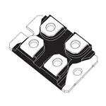
ISOTOP
INTERNAL SCHEMATIC DIAGRAM
APPLICATIONS
HIGH CURRENT, HIGH SPEED SWITCHING
n SWITH MODE POWER SUPPLIES (SMPS)
n DC-AC CONVERTERS FOR WELDING
EQUIPMENT AND UNINTERRUPTIBLE
POWER SUPPLIES AND MOTOR DRIVER
n
ABSOLUTE MAXIMUM RATINGS
Symbol
Value
Unit
Drain-source Voltage (VGS = 0)
500
V
Drain-gate Voltage (RGS = 20 kΩ)
500
V
Gate- source Voltage
±30
V
ID
Drain Current (continuos) at TC = 25°C
53
A
ID
Drain Current (continuos) at TC = 100°C
33
A
VDS
VDGR
VGS
IDM (l)
PTOT
dv/dt (1)
Parameter
Drain Current (pulsed)
212
A
Total Dissipation at TC = 25°C
460
W
Derating Factor
3.68
W/°C
Peak Diode Recovery voltage slope
VISO
Insulation Winthstand Voltage (AC-RMS)
Tstg
Storage Temperature
Tj
Max. Operating Junction Temperature
(•)Pulse width limited by safe operating area
May 2002
3
V/ns
2500
V
– 65 to 150
°C
150
°C
(1) ISD≤ 53A, di/dt≤100 A/µs, VDD≤ 24V, Tj≤TjMAX
1/8
�STE53NC50
THERMAL DATA
Rthj-case
Rthc-h
Thermal Resistance Junction-case
Max
0.272
°C/W
Thermal Resistance Case-heatsink with Conductive
Grease Applied
0.05
°C/W
AVALANCHE CHARACTERISTICS
Symbol
Parameter
IAR
Avalanche Current, Repetitive or Not-Repetitive
(pulse width limited by Tj max)
EAS
Single Pulse Avalanche Energy
(starting Tj = 25 °C, ID = IAR, VDD = 50 V)
Max Value
Unit
53
A
1043
mJ
ELECTRICAL CHARACTERISTICS (TCASE = 25 °C UNLESS OTHERWISE SPECIFIED)
OFF
Symbol
V(BR)DSS
IDSS
IGSS
Parameter
Test Conditions
Min.
Typ.
Max.
500
Unit
Drain-source
Breakdown Voltage
ID = 250 µA, VGS = 0
V
Zero Gate Voltage
Drain Current (VGS = 0)
VDS = Max Rating
10
µA
VDS = Max Rating, TC = 125 °C
100
µA
Gate-body Leakage
Current (VDS = 0)
VGS = ± 30V
±100
nA
ON (1)
Symbol
Parameter
Test Conditions
VGS(th)
Gate Threshold Voltage
VDS = VGS, ID = 250µA
RDS(on)
Static Drain-source On
Resistance
VGS = 10V, ID = 27A
Min.
Typ.
Max.
Unit
2
3
4
V
0.07
0.08
Ω
Typ.
Max.
Unit
DYNAMIC
Symbol
gfs (1)
Parameter
Forward Transconductance
Ciss
Input Capacitance
Coss
Output Capacitance
Crss
Reverse Transfer
Capacitance
Test Conditions
VDS > ID(on) x RDS(on)max,
ID = 15 A
VDS = 25V, f = 1 MHz, VGS = 0
Note: 1. Pulsed: Pulse duration = 300 µs, duty cycle 1.5 %.
2/8
Min.
42
S
11.2
nF
1350
pF
115
pF
�STE53NC50
ELECTRICAL CHARACTERISTICS (CONTINUED)
SWITCHING ON
Symbol
td(on)
tr
Parameter
Turn-on Delay Time
Rise Time
Qg
Total Gate Charge
Qgs
Gate-Source Charge
Qgd
Gate-Drain Charge
Test Conditions
Min.
VDD = 250V, ID = 26.5A
RG = 4.7Ω VGS = 10V
(see test circuit, Figure 3)
VDD = 400V, ID = 53A,
VGS = 10V
Typ.
Max.
Unit
46
ns
70
ns
310
434
nC
46
nC
150
nC
SWITCHING OFF
Symbol
tr(Voff)
Parameter
Off-voltage Rise Time
tf
Fall Time
tc
Cross-over Time
Test Conditions
Min.
VDD = 400V, ID = 53A,
RG = 4.7Ω, VGS = 10V
(see test circuit, Figure 5)
Typ.
Max.
Unit
45
ns
38
ns
85
ns
SOURCE DRAIN DIODE
Symbol
ISD
Parameter
Test Conditions
Min.
Typ.
Source-drain Current
ISDM (2)
Source-drain Current (pulsed)
VSD (1)
Forward On Voltage
ISD = 53A, VGS = 0
ISD = 53A, di/dt = 100A/µs,
VDD = 70V, Tj = 150°C
(see test circuit, Figure 5)
trr
Reverse Recovery Time
Qrr
Reverse Recovery Charge
IRRM
Reverse Recovery Current
Max.
Unit
53
A
212
A
1.6
V
760
ns
17.86
µC
47
A
Note: 1. Pulsed: Pulse duration = 300 µs, duty cycle 1.5 %.
2. Pulse width limited by safe operating area.
Safe Operating Area
Thermal Impedence
3/8
�STE53NC50
Output Characteristics
Transfer Characteristics
Transconductance
Static Drain-source On Resistance
Gate Charge vs Gate-source Voltage
Capacitance Variations
4/8
�STE53NC50
Normalized Gate Thereshold Voltage vs Temp.
Normalized On Resistance vs Temperature
Source-drain Diode Forward Characteristics
5/8
�STE53NC50
Fig. 1: Unclamped Inductive Load Test Circuit
Fig. 2: Unclamped Inductive Waveform
Fig. 3: Switching Times Test Circuit For
Resistive Load
Fig. 4: Gate Charge test Circuit
Fig. 5: Test Circuit For Inductive Load Switching
And Diode Recovery Times
6/8
�STE53NC50
ISOTOP MECHANICAL DATA
mm
DIM.
MIN.
A
TYP.
11.8
inch
MAX.
MIN.
TYP.
MAX.
12.2
0.466
0.480
B
8.9
9.1
0.350
0.358
C
1.95
2.05
0.076
0.080
D
0.75
0.85
0.029
0.033
E
12.6
12.8
0.496
0.503
F
25.15
25.5
0.990
1.003
G
31.5
31.7
1.240
1.248
H
4
J
4.1
4.3
0.161
0.169
K
14.9
15.1
0.586
0.594
L
30.1
30.3
1.185
1.193
M
37.8
38.2
1.488
1.503
8.2
0.307
0.157
N
4
O
7.8
0.157
0.322
A
G
B
O
F
E
H
D
N
J
K
C
L
M
7/8
�STE53NC50
Information furnished is believed to be accurate and reliable. However, STMicroelectronics assumes no responsibility for the
consequences of use of such information nor for any infringement of patents or other rights of third parties which may result from
its use. No license is granted by implication or otherwise under any patent or patent rights of STMicroelectronics. Specifications
mentioned in this publication are subject to change without notice. This publication supersedes and replaces all information
previously supplied. STMicroelectronics products are not authorized for use as critical components in life support devices or
systems without express written approval of STMicroelectronics.
© The ST logo is a registered trademark of STMicroelectronics
© 2002 STMicroelectronics - Printed in Italy - All Rights Reserved
STMicroelectronics GROUP OF COMPANIES
Australia - Brazil - Canada - China - Finland - France - Germany - Hong Kong - India - Israel - Italy - Japan - Malaysia - Malta - Morocco
Singapore - Spain - Sweden - Switzerland - United Kingdom - United States.
© http://www.st.com
8/8
�
很抱歉,暂时无法提供与“STE53NC50”相匹配的价格&库存,您可以联系我们找货
免费人工找货- 国内价格 香港价格
- 100+229.41243100+29.67800
- 国内价格
- 1+295.09001
- 5+253.11910
- 10+242.98571
- 20+233.39133
- 50+221.29355
- 100+212.27412
- 150+207.06369
- 200+203.33853
- 国内价格
- 1+321.12720
- 10+311.58000