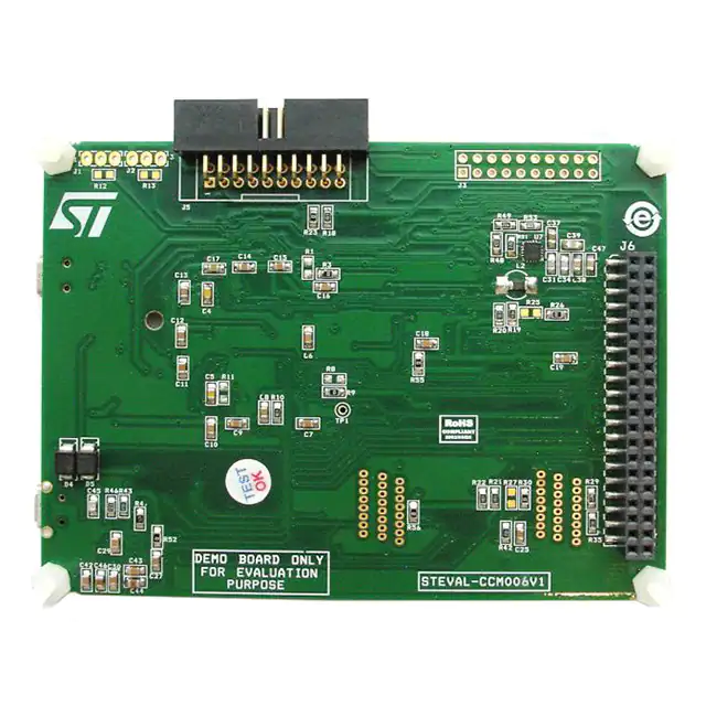
STEVAL-CCM006V1
STM32-based NAND Flash driver
evaluation board (without TFT)
Data brief
Description
The STEVAL-CCM006V1 is a product evaluation
board for a NAND Flash driver based on the
STM32F103ZET6 microcontroller.
It supports 512 byte and 2 kilobyte page SLC
NAND Flash, and dynamic detection of NAND
Flash based on “Device ID”.
The firmware automatically detects which NAND
Flash is mounted on the PCB, and functions
accordingly.
Features
• Designed for 512 byte and 2 kilobyte page size
NAND Flash interfacing using the FSMC
interface of the STM32
• Supports both FAT (ELM_FS) file system and
USB mass storage device mode
• Supports garbage collection, wear leveling,
bad block management & ECC check
• RoHS compliant
November 2013
DocID025388 Rev 1
For further information contact your local STMicroelectronics sales office.
1/7
www.st.com
�Schematic diagram
1
STEVAL-CCM006V1
Schematic diagram
3V3
PUSH BUT T ON
R4
10K
3V3
VDD_SA
VDD_3
PE1
PE0
PB9
PB8
BOOT0
PB7
PB6
PB5
PB4
PB3
PG15
VDD_11
VSS_11
PG14
PG13
PG12
PG11
PG10
PG9
PD7
PD6
VDD_10
VSS_10
PD5
PD4
PD3
PD2
PD1
PD0
PC12
PC11
PC10
PA15
PA14
U1
144
143
142
141
140
139
138
137
136
135
134
133
132
131
130
129
128
127
126
125
124
123
122
121
120
119
118
117
116
115
114
113
112
111
110
109
C1
100nF
D1
PE2
GND
1K
PE2
PE3
T EST _LED1
D2
R6
PE3
GND
1K
PF0_FSMC_ADDR_A0
T EST _LED2
C2
20pF
PH0_OSC_IN
GND
3V3
Y1
25MHz
R7
C3
20pF
PH1_OSC_OUT
PH0_OSC_IN
PH1_OSC_OUT
390
PC0_OTG_HS_ULPI_STP
NRST
PC2_OTG_HS_ULPI_DIR
PC3_OTG_HS_ULPI_NXT
For STM32F10xx
Y1----- 8MHz
For STM32F2xxx & STM32F4xxx
Y1------ 25MHz
GND
3V3
GND
R8
0 Ohm
3V3
R9
0 Ohm
VCAP
PE2
PE3
PE4
PE5
PE6
VBAT
PC13-TAMPER-RTC
PC14-OSC32_IN
PC15-OSC32_OUT
PF0
PF1
PF2
PF3
PF4
PF5
VSS_5
VDD_5
PF6
PF7
PF8
PF9
PF10
OSC_IN
OSC_OUT
NRST
PC0
PC1
PC2
PC3
VDD_12
VSSA
VREF+
VDDA
PA0_WKUP
PA1
PA2
STM32F103ZET6/
STM32F205ZET6/
STM32F405ZGT6
108
107
106
105
104
103
102
101
100
99
98
97
96
95
94
93
92
91
90
89
88
87
86
85
84
83
82
81
80
79
78
77
76
75
74
73
VDD_2
VSS_2
VCAP_2
PA13
PA12
PA11
PA10
PA9
PA8
PC9
PC8
PC7
PC6
VDD_9
VSS_9
PG8
PG7
PG6
PG5
PG4
PG3
PG2
PD15
PD14
VDD_8
VSS_8
PD13
PD12
PD11
PD10
PD9
PD8
PB15
PB14
PB13
PB12
3V3
GND
VCAP
PA13_JTAG_JTMS
PA12_OTG_FS_DP_USB
PA11_OTG_FS_DM_USB
PA10_OTG_FS_ID_USB
PA9_OTG_FS_VBUS_USB
3V3
GND
PG8_USB_PU
PG7_FSMC_INT3
PG6_FSMC_INT2
PD15_FSMC_D1
PD14_FSMC_D0
3V3
GND
PD12_FSMC_ADDR_A17
PD11_FSMC_ADDR_A16
PD10_FSMC_D15
PD9_FSMC_D14
PD8_FSMC_D13
PB13_OTG_HS_ULPI_D6
PB12_OTG_HS_ULPI_D5
37
38
39
40
41
42
43
44
45
46
47
48
49
50
51
52
53
54
55
56
57
58
59
60
61
62
63
64
65
66
67
68
69
70
71
72
T P1
1
2
3
4
5
6
7
8
9
10
11
12
13
14
15
16
17
18
19
20
21
22
23
24
25
26
27
28
29
30
31
32
33
34
35
36
PA3
VSS_4
VDD_4
PA4
PA5
PA6
PA7
PC4
PC5
PB0
PB1
PB2-BOOT1
PF11
PF12
VSS_6
VDD_6
PF13
PF14
PF15
PG0
PG1
PE7
PE8
PE9
VSS_7
VDD_7
PE10
PE11
PE12
PE13
PE14
PE15
PB10
PB11
VCAP_1
VDD_1
R5
PA15_JTAG_JTDI
PA14_JTAG_JTCK
R2
10K
PD1_FSMC_D3
PD0_FSMC_D2
R3
0 Ohm
PG10_FSMC_NE3
PG9_FSMC_NCE3
PD7_FSMC_NCE2
PD6_FSMC_NWAIT
3V3
GND
PD5_FSMC_NWE
PD4_FSMC_NOE
R1
0 Ohm
3V3
3V3
GND
PG14_TSCREEN_INT
NRST
GND
PB9
PB8
SW1
PB7_I2C1_SDA
PB6_I2C1_SCL
PB5_OTG_HS_ULPI_D7
PB4_JTAG_JNTRST
PB3_JTAG_JTDO
GND
Figure 1. Microcontroller section circuit schematic
GND
GND
3V3
GND
3V3
PB0_OTG_HS_ULPI_D1
PB1_OTG_HS_ULPI_D2
GND
PA5_OTG_HS_ULPI_CK
VCAP
R11
0 Ohm
GND
3V3
10K
R10
GND
3V3
For STM32F2xxx & STM32F4xxx
Mount --- R3,R9
DNM --- R1,R8,R11
J1
1
2
3
PA3_OTG_HS_ULPI_D0
For STM32F10xx
Mount --- R1,R8,R11
DNM --- R3,R9
PE10_FSMC_D7
PE11_FSMC_D8
PE12_FSMC_D9
PE13_FSMC_D10
PE14_FSMC_D11
PE15_FSMC_D12
PB10_OTG_HS_ULPI_D3
PB11_OTG_HS_ULPI_D4
T EST POINT
PE7_FSMC_D4
PE8_FSMC_D5
PE9_FSMC_D6
C5
2.2uF
3V3
1
C4
2.2uF
PB8
1K
CONN T RBLK 3
3V3
J2
1
2
3
C6
100nF
R13
3V3
C7
100nF
C8
100nF
C9
100nF
C10
100nF
C11
100nF
C12
100nF
C13
100nF
C14
100nF
C15
100nF
C16
100nF
C17
100nF
PB9
GND
1K
CONN T RBLK 3
GSPG15102013DI1510
Figure 2. NAND Flash circuit schematic
R56
3V3
R55
3V3
3V3_NAND2
3V3_NAND1
0 Ohm
0 Ohm
3V3_NAND1
R19
10K
3V3_NAND1
C18
100nF
R20
10K
3V3_NAND2
C19
100nF
GND
PD6_FSMC_NWA
IT
R25
0 Ohm
Mount One at a time
R28
R26
PD7_FSMC_NCE2
0 Ohm
22 Ohm
R33
R22
10K
R21
10K
C21
100nF
PG7_FSMC_I
NT3
PG6_FSMC_I
NT2
3V3_NAND1
3V3_NAND2
C20
100nF
PD4_FSMC_NOE
10K
3V3_NAND1
GND
PD11_FSMC_A
DDR_A16
PD12_FSMC_A
DDR_A17
PD5_FSMC_NWE
R41
3V3_NAND1
C24
100nF
10K
GND
GND
PD6_FSMC_NWA
IT
R27
U2
1
2
3
4
5
6
7
8
9
10
11
12
13
14
15
16
17
18
19
20
21
22
23
24
NC
NC
NC
NC
NC
NC
RB
R
E
NC
NC
VDD
VSS
NC
NC
CL
AL
W
WP
NC
NC
NC
NC
NC
NC
NC
NC
NC
I/O7
I/O6
I/O5
I/O4
NC
NC
NC
VDD
VSS
NC
NC
NC
I/O3
I/O2
I/O1
I/O0
NC
NC
NC
NC
48
47
46
45
44
43
42
41
40
39
38
37
36
35
34
33
32
31
30
29
28
27
26
25
PE10_FSMC_D7
PE9_FSMC_D6
PE8_FSMC_D5
PE7_FSMC_D4
R30
PG9_FSMC_NCE3
0 Ohm
22 Ohm
R35
3V3_NAND2
PD4_FSMC_NOE
10K
3V3_NAND1
GND
PD1_FSMC_D3
PD0_FSMC_D2
PD15_FSMC_D1
PD14_FSMC_D0
NAND512B
0 Ohm
Mount One at a time
R29
3V3_NAND2
GND
PD11_FSMC_A
DDR_A16
PD12_FSMC_A
DDR_A17
PD5_FSMC_NWE
R42
3V3_NAND2
C25
100nF
10K
GND
U3
1
2
3
4
5
6
7
8
9
10
11
12
13
14
15
16
17
18
19
20
21
22
23
24
NC
NC
NC
NC
NC
NC
RB
R
E
NC
NC
VDD
VSS
NC
NC
CL
AL
W
WP
NC
NC
NC
NC
NC
NC
NC
NC
NC
I/O7
I/O6
I/O5
I/O4
NC
NC
NC
VDD
VSS
NC
NC
NC
I/O3
I/O2
I/O1
I/O0
NC
NC
NC
NC
48
47
46
45
44
43
42
41
40
39
38
37
36
35
34
33
32
31
30
29
28
27
26
25
PE10_FSMC_D7
PE9_FSMC_D6
PE8_FSMC_D5
PE7_FSMC_D4
3V3_NAND2
GND
PD1_FSMC_D3
PD0_FSMC_D2
PD15_FSMC_D1
PD14_FSMC_D0
NAND512B
DNM: R25, R27
GSPG15102013DI1515
2/7
DocID025388 Rev 1
�STEVAL-CCM006V1
Schematic diagram
Figure 3. USB full speed circuit schematic
R14
PA12_OTG_FS_DP_USB
PG8_USB_PU
1.5k
USB5V_FS
C22
10uF
1
2
3
4
5
J4
USB_VCC
USBDM
USBDP
ID
USB_GND
SHELL
SHELL
SHELL
SHELL
6
7
8
9
USB_MINIA/B T YPE
PA9_OTG_FS_VBUS_USB
PA11_OTG_FS_DM_USB
PA12_OTG_FS_DP_USB
PA10_OTG_FS_ID_USB
R31
1M
R32
22
R34
22
R36
0 0
1
2
3
U4
I/O1
GND
I/O2
I/O1
VBUS
I/O2
6
5
4
C23
4.7nF
D3
R40
1k
USBLC6-2P6
LED_GREEN
GSPG15102013DI1520
Figure 4. JTAG connector circuit schematic
PB4_JTAG_JNTRST
PA14_JTAG_JTCK
PB3_JTAG_JTDO
NRST
PA13_JTAG_JTMS
PA15_JTAG_JTDI
J5
1
2
3
4
5
6
7
8
9
10
11
12
13
14
15
16
17
18
19
20
PB4_JTAG_JNTRST
PA14_JTAG_JTCK
PB3_JTAG_JTDO
NRST
PA13_JTAG_JTMS
PA15_JTAG_JTDI
3V3
R15
10k
R17
10k
R16
10k
R18
10k
R23
0 0
3V3
PB4_JTAG_JNTRST
R24
10k
PA15_JTAG_JTDI
PA13_JTAG_JTMS
NRST
PA14_JTAG_JTCK
RTCK
PB3_JTAG_JTDO
NRST
DBGRQ
DBGACK
R38
10k
R39
10k
R37
10k
JT AG_CONN
GSPG15102013DI1525
DocID025388 Rev 1
3/7
7
�Schematic diagram
STEVAL-CCM006V1
XTAL1
XTAL2
3V3_HS
Figure 5. USB high speed circuit schematic
C27
C28 C29
0.1uF 0.1uF 0.1uF
C30
R43
10K
0.1uF
+ +
C36
24
23
22
21
20
19
18
17
31
16
6
30
25
27
28
4.7uF
33
1
2
3
10
32
4
8
7
5
GNDPAD
GND
GND
CPEN
EXTVBUS
RBIAS
VBUS
DM
DP
ID
DATA0
DATA1
DATA2
DATA3
DATA4
DATA5
DATA6
DATA7
D6
1K
LED_GREEN
R46
J7
12K
USB5V_HS
820
R47
XTAL1
Y2
24MHz
C45
33pF
R50
1M
XTAL2
PC3_OTG_HS_ULPI_NXT
PC2_OTG_HS_ULPI_DIR
PC0_OTG_HS_ULPI_STP
PA5_OTG_HS_ULPI_CK
USB3300
C41
33pF
1
2
3
4
5
USB_VCC
USBDM
USBDP
ID
USB_GND
SHELL
SHELL
L1
6
7
BEAD
9
11
12
13
14
15
29
26
RESET
NXT
DIR
STP
CLKOUT
VDD1.8
VDDA1.8
VDD1.8
PA3_OTG_HS_ULPI_D0
PB0_OTG_HS_ULPI_D1
PB1_OTG_HS_ULPI_D2
PB10_OTG_HS_ULPI_D3
PB11_OTG_HS_ULPI_D4
PB12_OTG_HS_ULPI_D5
PB13_OTG_HS_ULPI_D6
PB5_OTG_HS_ULPI_D7
R44
REG_EN
VDD3.3
VDD3.3
VDD3.3
VDD3.3
XO
XI
U6
C46
C42
0.1uF
C43
C44
4.7uF
0.1uF
4.7uF
R52
0 0
3V3
3V3_HS
GSPG15102013DI1530
Figure 6. Touch screen controller circuit schematic
AGND
AGND
TSC_YD
C34
2pF
AGND
R57
GND
0 0
AGND
TSC_XR
9
IN1
11
10
GND
IN2
SCLK
VCC
SDAT
8
7
3V3
6
C39
100nF
SDAT
5
AGND
C40
10uF
3V3
4
A0
Y-
X-
1
TSC_YD
STMPE811
3
16
AGND
Y+
DATA_IN
R48
4.7K
SCLK
AGND
TSC_XL
15
12
AGND
TSC_YU
TSC_YU
IN0
VIO
INT
BEAD
C38
100nF
X+
2
C37
1uF
14
PG14_TSCREEN_INT
L2
3V3
13
IN3
U7
TSC_XR
C33
2pF
C32
2pF
TSC_XL
C31
2pF
R54
10k
3V3
SCLK
R51
SDAT
R53
22
22
R49
4.7K
PB6_I2C1_SCL
PB7_I2C1_SDA
C47
100nF
AGND
GSPG15102013DI1535
4/7
DocID025388 Rev 1
�STEVAL-CCM006V1
Schematic diagram
Figure 7. Power section circuit schematic
D4
3V3
USB5V_FS
ST PS1L30U
GND
1
2
3
4
D5
5V0
USB5V_HS
ST PS1L30U
C48
10uF
U5
GND
VOUT
VOUT
VIN
8
7
6
5
C26
10uF
LD1117D33T R
C35
100nF
R45
NC
VOUT
VOUT
NC
D7
GND
3V3
1k
LED_GREEN
GSPG15102013DI1540
Figure 8. TFT connector circuit schematic
J6
PG10_FSMC_NE3
PD5_FSMC_NWE
NRST
PD15_FSMC_D1
PD1_FSMC_D3
PE8_FSMC_D5
PE10_FSMC_D7
PE12_FSMC_D9
PE14_FSMC_D11
PD8_FSMC_D13
PD10_FSMC_D15
5V0
3V3
GND
TSC_XL
TSC_YD
1
3
5
7
9
11
13
15
17
19
21
23
25
27
29
31
33
35
37
39
2
4
6
8
10
12
14
16
18
20
22
24
26
28
30
32
34
36
38
40
PF0_FSMC_ADDR_A0
PD4_FSMC_NOE
PD14_FSMC_D0
PD0_FSMC_D2
PE7_FSMC_D4
PE9_FSMC_D6
PE11_FSMC_D8
PE13_FSMC_D10
PE15_FSMC_D12
PD9_FSMC_D14
GND
3V3
GND
5V0
TSC_XR
TSC_YU
CONNECT OR20x2
GSPG15102013DI1545
Figure 9. NAND signals circuit schematic
J3
PD14_FSMC_D0
PD15_FSMC_D1
PD0_FSMC_D2
PD1_FSMC_D3
PE7_FSMC_D4
PE8_FSMC_D5
PE9_FSMC_D6
PE10_FSMC_D7
PD11_FSMC_ADDR_A16
PD12_FSMC_ADDR_A17
PD4_FSMC_NOE
PD5_FSMC_NWE
PD7_FSMC_NCE2
PG9_FSMC_NCE3
PG6_FSMC_INT2
PG7_FSMC_INT3
PD6_FSMC_NWAIT
GND
3V3
GND
1
2
3
4
5
6
7
8
9
10
11
12
13
14
15
16
17
18
19
20
CON20
DocID025388 Rev 1
GSPG15102013DI1550
5/7
7
�Revision history
2
STEVAL-CCM006V1
Revision history
Table 1. Document revision history
6/7
Date
Revision
11-Nov-2013
1
Changes
Initial release.
DocID025388 Rev 1
�STEVAL-CCM006V1
Please Read Carefully:
Information in this document is provided solely in connection with ST products. STMicroelectronics NV and its subsidiaries (“ST”) reserve the
right to make changes, corrections, modifications or improvements, to this document, and the products and services described herein at any
time, without notice.
All ST products are sold pursuant to ST’s terms and conditions of sale.
Purchasers are solely responsible for the choice, selection and use of the ST products and services described herein, and ST assumes no
liability whatsoever relating to the choice, selection or use of the ST products and services described herein.
No license, express or implied, by estoppel or otherwise, to any intellectual property rights is granted under this document. If any part of this
document refers to any third party products or services it shall not be deemed a license grant by ST for the use of such third party products
or services, or any intellectual property contained therein or considered as a warranty covering the use in any manner whatsoever of such
third party products or services or any intellectual property contained therein.
UNLESS OTHERWISE SET FORTH IN ST’S TERMS AND CONDITIONS OF SALE ST DISCLAIMS ANY EXPRESS OR IMPLIED
WARRANTY WITH RESPECT TO THE USE AND/OR SALE OF ST PRODUCTS INCLUDING WITHOUT LIMITATION IMPLIED
WARRANTIES OF MERCHANTABILITY, FITNESS FOR A PARTICULAR PURPOSE (AND THEIR EQUIVALENTS UNDER THE LAWS
OF ANY JURISDICTION), OR INFRINGEMENT OF ANY PATENT, COPYRIGHT OR OTHER INTELLECTUAL PROPERTY RIGHT.
ST PRODUCTS ARE NOT DESIGNED OR AUTHORIZED FOR USE IN: (A) SAFETY CRITICAL APPLICATIONS SUCH AS LIFE
SUPPORTING, ACTIVE IMPLANTED DEVICES OR SYSTEMS WITH PRODUCT FUNCTIONAL SAFETY REQUIREMENTS; (B)
AERONAUTIC APPLICATIONS; (C) AUTOMOTIVE APPLICATIONS OR ENVIRONMENTS, AND/OR (D) AEROSPACE APPLICATIONS
OR ENVIRONMENTS. WHERE ST PRODUCTS ARE NOT DESIGNED FOR SUCH USE, THE PURCHASER SHALL USE PRODUCTS AT
PURCHASER’S SOLE RISK, EVEN IF ST HAS BEEN INFORMED IN WRITING OF SUCH USAGE, UNLESS A PRODUCT IS
EXPRESSLY DESIGNATED BY ST AS BEING INTENDED FOR “AUTOMOTIVE, AUTOMOTIVE SAFETY OR MEDICAL” INDUSTRY
DOMAINS ACCORDING TO ST PRODUCT DESIGN SPECIFICATIONS. PRODUCTS FORMALLY ESCC, QML OR JAN QUALIFIED ARE
DEEMED SUITABLE FOR USE IN AEROSPACE BY THE CORRESPONDING GOVERNMENTAL AGENCY.
Resale of ST products with provisions different from the statements and/or technical features set forth in this document shall immediately void
any warranty granted by ST for the ST product or service described herein and shall not create or extend in any manner whatsoever, any
liability of ST.
ST and the ST logo are trademarks or registered trademarks of ST in various countries.
Information in this document supersedes and replaces all information previously supplied.
The ST logo is a registered trademark of STMicroelectronics. All other names are the property of their respective owners.
© 2013 STMicroelectronics - All rights reserved
STMicroelectronics group of companies
Australia - Belgium - Brazil - Canada - China - Czech Republic - Finland - France - Germany - Hong Kong - India - Israel - Italy - Japan Malaysia - Malta - Morocco - Philippines - Singapore - Spain - Sweden - Switzerland - United Kingdom - United States of America
www.st.com
DocID025388 Rev 1
7/7
7
�
很抱歉,暂时无法提供与“STEVAL-CCM006V1”相匹配的价格&库存,您可以联系我们找货
免费人工找货