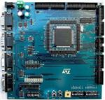
STEVAL-IFN001V2
Low cost starter development kit based on ST10F276Z5,
oriented to multi-axis motion control
Data Brief
Features
■
RS232
■
RS485
■
2 CAN
■
I2C (3.3 V and 5 V)
■
MC connector
■
3 powerSPIN connectors
■
VN808 board connector
Description
This two-layer, cost-effective development board
is based on the ST10F276Z5 Flash memory
microcontroller with DSP functionalities, suitable
for the development of motion control
applications. The board can be easily
interconnected with different kinds of motor
drivers through to a series of connectors available
on board. In particular, three dedicated
connectors allow the user to manage
STMicroelectronics powerSPIN evaluation boards
(which are integrated monolithic motor drivers)
while interfacing with any board that is compatible
with this ST standard connector through the MCconnector. It is also possible to drive high loads by
using an output connector compatible with VN808
and VN340 reference design boards.
October 2007
STEVAL-IFN001V2
Rev 1
For further information contact your local STMicroelectronics sales office.
1/5
www.st.com
5
�Schematic 1
Figure 1.
P6.0
P6.2
P6.4
P6.6
P8.0
P8.2
P8.4
P8.6
+5V
P7.0
P7.2
P7.4
P7.6
P5.0
P5.2
P5.4
P5.6
P5.8
1
3
5
7
9
11
13
15
17
19
21
23
25
27
29
31
33
35
U14
2
4
6
8
10
12
14
16
18
20
22
24
26
28
30
32
34
36
CON36_A
CON4
1
2
3
4
J3
P6.1
P6.3
P6.5
P6.7
P8.1
P8.3
P8.5
P8.7
GND
P7.1
P7.3
P7.5
P7.7
P5.1
P5.3
P5.5
P5.7
P5.9
GND
VAREF
P5.10
P5.12
P5.14
GND
P2.0
P2.2
P2.4
P2.6
GND
P2.8
P2.10
P2.12
P2.14
P3.0
P3.2
P3.4
1
3
5
7
9
11
13
15
17
19
21
23
25
27
29
31
33
35
U15
2
4
6
8
10
12
14
16
18
20
22
24
26
28
30
32
34
36
CON36_A
PFC Sync
PFC PWM
ENCODER_A
ENCODER_B
Fault
PWM_1H
PWM_1L
PWM_2H
PWM_2L
PWM_3H
PWM_3L
Current Phase_A
Current Phase_B
Current Phase_C
NTC bypass Relay
Dissipative brake PWM
2
4
6
8
10
12
14
16
18
20
22
24
26
28
30
32
34
2
2
4
6
8
10
12
14
16
18
20
22
24
26
28
30
32
34
GND
P5.11
P5.13
P5.15
+5V
P2.1
P2.3
P2.5
P2.7
V18
P2.9
P2.11
P2.13
P2.15
P3.1
P3.3
P3.5
+5V
J200
1
3
5
7
9
11
13
15
17
19
21
23
25
27
29
31
33
CON34A
P2.10
P0L.0
P0L.3
P0L.6
P6.0
P2.0
P8.0 P
P7.4
P7.0 P
P2.3
GND
P3.6
P3.8
P3.10
P3.12
P3.15
GND
P4.0
P4.2
P4.4
P4.6
+5V
RD/
READY/
EA/
P0L.1
P0L.3
P0L.5
P0L.7
Bus Voltage
GND
P5.4
1
3
5
7
9
11
13
15
17
19
21
23
25
27
29
31
33
35
P5.3
+ 3.3 V
P2.8
Heatsink Temperature
GND
ENCODER_INDEX
+5V
U16
2
4
6
8
10
12
14
16
18
20
22
24
26
28
30
32
34
36
CON36_A
P5.6
P1L.1
GND
P2.14
P1H.5
P3.7
P3.9
P3.11
P3.13
+5V
RPD
P4.1
P4.3
P4.5
P4.7
GND
WRL/
ALE
P0L.0
P0L.2
P0L.4
P0L.6
P0H.0
J208
JUMPER
J203
1
3
5
7
9
11
13
15
17
19
21
23
25
27
29
31
33
2
4
6
8
10
12
14
16
18
20
22
24
26
28
30
32
34
+5V
1
3
5
7
9
11
13
15
17
19
21
23
25
27
29
31
33
35
P2.4
P7.5
P7.1 P
P2.1
P8.1 P
P6.1
P0L.4
P0L.7
P2.11
P0L.1
GND
P0H.1
P0H.3
P0H.5
P0H.7
P1L.1
P1L.3
P1L.5
P1L.7
GND
P1H.1
P1H.3
P1H.5
P1H.7
XTAL2
GND
RSTOUT/
CON34A
U17
2
4
6
8
10
12
14
16
18
20
22
24
26
28
30
32
34
36
CON36_A
GND
+5V
1
P0H.2
P0H.4
P0H.6
P1L.0
P1L.2
P1L.4
P1L.6
+5V
P1H.0
P1H.2
P1H.4
P1H.6
+5V
XTAL1
RSTIN/
NMI/
+5V
J210
2
JUMPER
2
P2.15
P1H.6
GND
P1L.2
P5.7
1
+ 12 V
+5V
P2.9
P7.0 V
P8.0 V
P7.1 V
P8.1V
P7.2 V
P8.2V
P5.0
P5.1
P5.2
P6.7
P8.3
+5V
P4.3
P7.3
P3.6 V
P3.4 V
J207
JUMPER
J202
1
3
5
7
9
11
13
15
17
19
21
23
25
27
29
31
33
CON34A
2
1
D
3.3 V
+5V
GND
P1L.0
P5.5
2
1
P2.13
P1H.4
P6.4
P0H.1
P0H.3
P0H.5
P0H.7
J209
JUMPER
1
3
5
7
9
11
13
J205
1
3
5
7
9
11
13
15
17
19
21
23
25
27
29
31
33
J201
2
4
6
8
10
12
14
16
18
20
22
24
26
28
30
32
34
CON14A
CON34A
2
4
6
8
10
12
14
P0H.0
P0H.2
P0H.4
P0H.6
P2.12
P0L.2
P0L.5
P6.3
P6.2
P2.2
P8.2 P
P7.6
P7.2 P
P2.5
1
J211
2
JUMPER
GND
P7.0 P
P7.1 P
P7.2 P
P8.0 P
P8.1 P
P8.2 P
P3.4 P
P3.6 P
P7.0
P7.1
P7.2
P8.0
P8.1
P8.2
P3.4
P3.6
P7.0 V
P7.1 V
P7.2 V
P8.0 V
P8.1V
P8.2V
P3.4 V
P3.6 V
1
2
3
4
5
6
7
8
9
10
11
12
13
14
15
16
17
18
19
20
21
22
23
24
J206
CON24
2/5
Block diagram
1
STEVAL-IFN001V2
Block diagram
�Schematic 2
1
R22
1K
1
1
1
3
2
U3
XTAL1
XTAL2
GND
XTAL1
XTAL2
NMI/
RSTOUT/
RSTIN/
1
XTAL1
C6
15pF
GND
+5V
1
2
J1
1
XTAL2
GND
D5
LM4040
J6
GND
GND
CON2
1
2
1
2
J2
CON2
VAREF
C24
2
100nF
GND
C7
15pF
0
R19
CON2
1N4001
D12
100nF
C25
10K Trimmer
R20
2
+
C31
100nF
GND
P8.6
P2.15
P8.7
GND
100nF
P3.10
100nF
1
1
C1
C4
TXD0
P3.11 RXD0
9
12
10
11
5
3
24
2 1
+5V
JUMPER JP5
1
2
JP6
2
2
JUMPER
JUMPER
1
1
JP7
GND
1
2
3
4
5
6
7
8
2
1
U2
C1+
C1C2+
T2in
T1in
R2in
R1in
T2out
T1out
V-
V+
ST202E
R1out
C2-
R2out
100nF
C9
GND
+5V
100nF
C10
B
A
GND
+5V
ST485A
VCC
U7 GND
RO
RE
DE
DI
16
15
14
13
12
11
10
9
16
15
14
13
12
11
10
9
SW DIP-8
SW5
SW DIP-8
SW3
R10
390R
4
3
1
2
3
4
5
6
7
8
GND
6
2
1
1
1
1K
R1
2
RXD0*
TXD0*
DTR0*
C2 100nF
2 +5V
C3 100nF
2
GND
R5
220R
1
6
2
7
3
8
4
9
5
R13
390R
1
6
2
7
3
8
4
9
5
P2
Case to
Ground
+5V
Case to
Ground
P4
JUMPER
JP8
JUMPER
JP3
390R
R4
GND
RXD0*
7
8
13
8
7
6
GND
P0H.0
P0H.1
P0H.2
P0H.3
P0H.4
P0H.5
P0H.6
P0H.7
P0L.0
P0L.1
P0L.2
P0L.3
P0L.4
P0L.5
P0L.6
P0L.7
R12
0R
2
2
2
2
2
2
2
2
2
2
2
2
2
2
2
2
GND
R33
R35
R36
R38
R39
R41
R42
R46
R23
R24
R25
R26
R27
R28
R29
R30
5
GND
R11
0R
1
1
1
1
1
1
1
1
1
1
1
1
1
1
1
1
JP4
14 TXD0*
JUMPER
144
143
138
137
142
141
140
P1H.7
P1H.6
P1H.5
P1H.4
P1H.3
P1H.2
P1H.1
P1H.0
P1L.7
P1L.6
P1L.5
P1L.4
P1L.3
P1L.2
P1L.1
P1L.0
+5V
1uF
C13
GND
GND
Vin
+ 12 V
STLF50CDT
VAREF
U13
Vout
1
XTAL4
XTAL3
NMI
RSTOUT
RSTIN
135
134
133
132
131
130
129
128
125
124
123
122
121
120
119
118
EA/
ALE
READY/
WRL/
RD/
P0H.7
P0H.6
P0H.5
P0H.4
P0H.3
P0H.2
P0H.1
P0H.0
P0L.7
P0L.6
P0L.5
P0L.4
P0L.3
P0L.2
P0L.1
P0L.0
99
98
97
96
95
P4.7
P4.6
P4.5
P4.4
P4.3
P4.2
P4.1
P4.0
117
116
115
114
113
112
111
108
107
106
105
104
103
102
101
100
92
91
90
89
88
87
86
85
RPD
GND
VSS
+5V
VDD
V18
10nF
C14
RPD
84
GND
RSTIN/
+5V
17
46
72
82
93
109
126
136
18
45
55
71
83
94
110
127
139
56
2
4
3
GND
C30
100uF
2
P6.0/CS0
P6.1/CS1
P6.2/CS2
P6.3/CS3
P6.4/CS4
P6.5/HOLD/SCLK1
P6.6/HLDA/MTSR1
P6.7/BREQ/MRST1
P1H.7/A15/CC27I
P1H.6/A14/CC26I
P1H.5/A13/CC25I
P1H.4/A12/CC24I
P1H.3/A11
P1H.2/A10
P1H.1/A9
P1H.0/A8
P1L.7/A7/AN23
P1L.6/A6/AN22
P1L.5/A5/AN21
P1L.4/A4/AN20
P1L.3/A3/AN19
P1L.2/A2/AN18
P1L.1/A1/AN17
P1L.0/A0/AN16
VCC
V18
VSS
VSS
VSS
VSS
VSS
VSS
VSS
VSS
VSS
VDD
VDD
VDD
VDD
VDD
VDD
VDD
VDD
U10
GND RST
MR
stm811
+5V
+
GND
+5V
+5V
P4.7
P4.4
1
C5
100nF
1
4
3
2
8
1
4
3
2
8
U4
TXD CANH
RXD CANL
VCC
GND
RS
REF
L9616
U5
TXD CANH
RXD CANL
VCC
GND
RS
REF
L9616
CAN2RX
CAN2TX
GND
C11
100nF
SDA
SCL
GND
1
R44
7
6
5
7
6
5
10nF
C32
1
120
R2
CAN H2
CAN L2
JP10
1
3
5
7
9
11
13
15
17
19
21
23
JUMPER
JP1
2
2 1
2
GND
CAN L1
CAN H1
CAN L2
GND
GND
1
2
3
4
5
6
7
CAN H2
ST3378E
I2C 3V
GND
+5V
JF1 SDA 3.3
1
2 1 SCL 3.3
3
4 3
5
6 5
RSTOUT/
2
4
6
VCC
VL
I/O VCC1
I/O VL1
I/O VCC2
I/O VL2
I/O VCC3
I/O VL3
I/O VCC4
I/O VL4
n.c.
n.c.
OE
GND
U6
JUMPER
JP2
CAN H1
CAN L1
1 1
14
13
12
11
10
9
8
OE
I2C 5V
+5V
GND
SDA 5
SCL 5
2
1
C23
100nF
GND
11
U11D
2
4
6
8
10
12
14
16
18
20
22
24
74HCF132
2
4
6
8
10
12
14
16
18
20
22
24
2 R3
120
U11A
12
13
1
3
5
7
9
11
13
15
17
19
21
23
74HCF132
3
JP9
OE
2
For 3.3 I2C
JUMPER
GND
1
+5V
GND
1
3
GND
2
U8
1
1
3
I2C
2
U9
1
I2C
1.5K
R16
SW6
2
D11
D10
D9
1.5K
R17
D6
D4
D3
D8
D7
5
4
GP Button
U11B
2
2
GND
C8
100nF
CAN2TX
CAN2RX
GND
P4.6
P4.5
+5V
+5V
R15
+ 3.3 V
EINIT
POWER
1K
D1
D2
R21
1
9
2
3
4
5
6
7
8
C
1.5K RSip
6
R43
74HCF132
2
1
GND
1
GND
15
1
2
3
4
5
6
7
8
P8.0/XPOUT0/CC16IO
P8.1/XPOUT1/CC17IO
P8.2/XPOUT2/CC18IO
P8.3/XPOUT3/CC19IO
P8.4/CC20IO
P8.5/CC21IO
P8.6/RxD1/CC22IO
P8.7/TxD1/CC23IO
P7.0/POUT0
P7.1/POUT1
P7.2/POUT2
P7.3/POUT3
P7.4/CC28IO
P7.5/CC29IO
P7.6/CC30IO
P7.7/CC31IO
GND
1
3
P5.0/AN0
P0H.7/AD15
P5.1/AN1
P0H.6/AD14
P5.2/AN2
P0H.5/AD13
P5.3/AN3
P0H.4/AD12
P5.4/AN4
P0H.3/AD11
P5.5/AN5
P0H.2/AD10
P5.6/AN6
P0H.1/AD9
P5.7/AN7
P0H.0/AD8
P5.8/AN8
P0L.7/AD7
P5.9/AN9
P0L.6/AD6
P0L.5/AD5
VAREF
P0L.4/AD4
VAGND
P0L.3/AD3
P0L.2/AD2
P0L.1/AD1
P5.10/AN10/T6EUD
P0L.0/AD0
P5.11/AN11/T5EUD
P5.12/AN12/T6IN
EA/VSTBY
P5.13/AN13/T5IN
ALE
P5.14/AN14/T4EUD
READY
P5.15/AN15/T2EUD
WR/WRL
RD
P2.0/CC0IO
P2.1/CC1IO
P4.7/A23/CAN2_TxD/SDA
P2.2/CC2IO
P4.6/A22/CAN1_TxD/CAN2_TxD
P2.3/CC3IO
P4.5/A21/CAN1_RxD/CAN2_RxD
P2.4/CC4IO
P4.4/A20/CAN2_RxD/SCL
P2.5/CC5IO
P4.3/A19
P2.6/CC6IO
P4.2/A18
P2.7/CC7IO
P4.1/A17
P2.8/CC8IO/EX0IN
P4.0/A16
P2.9/CC9IO/EX01IN
P2.10/CC10IO/EX02IN
RPD
P2.11/CC11IO/EX03IN
P2.12/CC12IO/EX04IN
P2.13/CC13IO/EX05IN
P2.14/CC14IO/EX06IN
P2.15/CC15IO/EX07IN/T7IN
P3.0/T0IN
P3.1/T6OUT
P3.2/CAPIN
P3.3/T3OUT
P3.4/T3EUD
P3.5/T4IN
P3.6/T3IN
P3.7/T2IN
P3.8/MRST0
P3.9/MTSR0
P3.10/TXD0
P3.11/RXD0
P3.12/BHE/WRH
P3.13/SCLK0
P3.15/CLKOUT
SW1
GND
1
STLF33CDT
Vin
C29
100nF
16
2
1
2
1
2
P6.0
P6.1
P6.2
P6.3
P6.4
P6.5
P6.6
P6.7
19
20
21
22
23
24
25
26
9
10
11
12
13
14
15
16
P7.0
P7.1
P7.2
P7.3
P7.4
P7.5
P7.6
P7.7
27
28
29
30
31
32
33
34
35
36
GND
+ 3.3 V
U12
Vout
GND GND
9
10
GND
1
6
2
7
3
8
4
9
5
1
6
2
7
3
8
4
9
5
2
SW2
P1
Case to
Ground
P3
Case to
Ground
C12
100nF
+ 3.3 V
GND
GND
8
16
15
14
13
12
11
10
9
10K RSip
R18
GND
1
2
3
4
5
6
7
8
U11C
SW DIP-8
74HCF132
1
2
P8.0
P8.1
P8.2
P8.3
P8.4
P8.5
P8.6
P8.7
P5.0
P5.1
P5.2
P5.3
P5.4
P5.5
P5.6
P5.7
P5.8
P5.9
39
40
41
42
43
44
VAREF
GND
P5.10
P5.11
P5.12
P5.13
P5.14
P5.15
+5V
EA/
+5V
3
+
1
C28
470uF
2
1
2
1
4.7K
R8
4.7K
R9
1
2
4.7K
R6
4.7K
R7
1
2
1
VCC
2
1
2
1
1
2
1
37
38
SW4
2
1
2
3
2
2
2
2
2
10K
10K
R37
R40
2
10K
R31
10K
R32
10K
R34
1
1
10K
R45
GND
C27
100uF
2
1
1
220K
R14
1
2
47
48
49
50
51
52
53
54
57
58
59
60
61
62
63
64
1
1
1
65
66
67
68
69
70
73
74
75
76
77
78
79
80
81
1
2
2
P2.0
P2.1
P2.2
P2.3
P2.4
P2.5
P2.6
P2.7
P2.8
P2.9
P2.10
P2.11
P2.12
P2.13
P2.14
P2.15
P3.0
P3.1
P3.2
P3.3
P3.4
P3.5
P3.6
P3.7
P3.8
P3.9
P3.10
P3.11
P3.12
P3.13
P3.15
VDD
C19 C20 C21 C22
100nF 100nF 100nF 100nF
+5V
2
C100
100nF C15 C16 C17 C18
100nF 100nF 100nF 100nF
1
GND
2
GND GND GND GND GND GND GND GND
EA/
READY/
WRL/
RSTOUT/
NMI/
P3.12 WRH/
GND
9
8
7
6
5
4
3
2
1
7
14
1
GND
1
2
1
1
2
1
1
2
1
2
3
1
2
2
2
2
4
1
2
4
2
C26
100nF
1
2
1
3
1
1
2
gnd
2
1
2
2
1
2
1
2
gnd
2
2
2
ST10F276
3
1
2
C
Figure 2.
Block diagram
STEVAL-IFN001V2
3/5
�Revision history
2
STEVAL-IFN001V2
Revision history
Table 1.
4/5
Document revision history
Date
Revision
26-Oct-2007
1
Changes
Initial release
�STEVAL-IFN001V2
Please Read Carefully:
Information in this document is provided solely in connection with ST products. STMicroelectronics NV and its subsidiaries (“ST”) reserve the
right to make changes, corrections, modifications or improvements, to this document, and the products and services described herein at any
time, without notice.
All ST products are sold pursuant to ST’s terms and conditions of sale.
Purchasers are solely responsible for the choice, selection and use of the ST products and services described herein, and ST assumes no
liability whatsoever relating to the choice, selection or use of the ST products and services described herein.
No license, express or implied, by estoppel or otherwise, to any intellectual property rights is granted under this document. If any part of this
document refers to any third party products or services it shall not be deemed a license grant by ST for the use of such third party products
or services, or any intellectual property contained therein or considered as a warranty covering the use in any manner whatsoever of such
third party products or services or any intellectual property contained therein.
UNLESS OTHERWISE SET FORTH IN ST’S TERMS AND CONDITIONS OF SALE ST DISCLAIMS ANY EXPRESS OR IMPLIED
WARRANTY WITH RESPECT TO THE USE AND/OR SALE OF ST PRODUCTS INCLUDING WITHOUT LIMITATION IMPLIED
WARRANTIES OF MERCHANTABILITY, FITNESS FOR A PARTICULAR PURPOSE (AND THEIR EQUIVALENTS UNDER THE LAWS
OF ANY JURISDICTION), OR INFRINGEMENT OF ANY PATENT, COPYRIGHT OR OTHER INTELLECTUAL PROPERTY RIGHT.
UNLESS EXPRESSLY APPROVED IN WRITING BY AN AUTHORIZED ST REPRESENTATIVE, ST PRODUCTS ARE NOT
RECOMMENDED, AUTHORIZED OR WARRANTED FOR USE IN MILITARY, AIR CRAFT, SPACE, LIFE SAVING, OR LIFE SUSTAINING
APPLICATIONS, NOR IN PRODUCTS OR SYSTEMS WHERE FAILURE OR MALFUNCTION MAY RESULT IN PERSONAL INJURY,
DEATH, OR SEVERE PROPERTY OR ENVIRONMENTAL DAMAGE. ST PRODUCTS WHICH ARE NOT SPECIFIED AS "AUTOMOTIVE
GRADE" MAY ONLY BE USED IN AUTOMOTIVE APPLICATIONS AT USER’S OWN RISK.
Resale of ST products with provisions different from the statements and/or technical features set forth in this document shall immediately void
any warranty granted by ST for the ST product or service described herein and shall not create or extend in any manner whatsoever, any
liability of ST.
ST and the ST logo are trademarks or registered trademarks of ST in various countries.
Information in this document supersedes and replaces all information previously supplied.
The ST logo is a registered trademark of STMicroelectronics. All other names are the property of their respective owners.
© 2007 STMicroelectronics - All rights reserved
STMicroelectronics group of companies
Australia - Belgium - Brazil - Canada - China - Czech Republic - Finland - France - Germany - Hong Kong - India - Israel - Italy - Japan Malaysia - Malta - Morocco - Singapore - Spain - Sweden - Switzerland - United Kingdom - United States of America
www.st.com
5/5
�
很抱歉,暂时无法提供与“STEVAL-IFN001V2”相匹配的价格&库存,您可以联系我们找货
免费人工找货- 国内价格
- 1+3961.24560
- 200+1580.56920
- 500+1527.74640
- 1000+1501.65360