UM0971
User manual
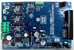
STEVAL-IHM031V1 low voltage
three-phase inverter demonstration board
Introduction
The STEVAL-IHM031V1 demonstration board is a low voltage three-phase power stage
inverter designed to perform permanent magnet motor controls. To this purpose, it must be
connected to an additional control logic stage (usually based on an 8/32-bit microcontroller).
According to the existing wide range of motor types and control techniques, it has been
designed to offer large flexibility by allowing full configurability.
In particular, it can be used for implementing scalar control (also known as current six-step
mode or trapezoidal shaped back-EMF) and field oriented control (sinusoidal-shaped backEMF PMSM).
The system has been specifically designed to achieve accurate and fast conditioning of the
current and back-EMF feedbacks, thereby matching the requirements typical of high-end
applications such as field oriented motor control. Back-EMF conditioning networks can
include an amplification stage for managing very low motor speed. Circuit networks are
provided to implement different techniques of sensorless speed and rotor position detection.
The input voltage range is from 12 V up to 24 V with no need to set any jumper for selecting
the input voltage level. Nominal power is up to 120 W. A dedicated power supply has been
designed to provide power +5 V and +3.3 V voltages to supply the control stage board. The
latter can be connected to the STEVAL-IHM031V1 board by using a dedicated motor control
connector, generally available in most boards based on microcontrollers produced by ST.
The three-phase inverter bridge is based on the STS8DNH3LL power MOSFET dual-inpackage SO-8 and L6387E gate driver. The board is self-protected by overcurrent events
and for each power MOSFET the case temperature is sensed through a temperature
sensor. A connector exists to read signals coming from encoder and Hall sensors.
Figure 1.
October 2010
STEVAL-IHM031V1 demonstration board
Doc ID 17701 Rev 1
1/45
www.st.com
�Contents
UM0971
Contents
1
2
STEVAL-IHM031V1 features . . . . . . . . . . . . . . . . . . . . . . . . . . . . . . . . . . . 6
1.1
Electrical and functional characteristics . . . . . . . . . . . . . . . . . . . . . . . . . . . 6
1.2
Target application . . . . . . . . . . . . . . . . . . . . . . . . . . . . . . . . . . . . . . . . . . . . 6
1.3
Safety and operating instructions . . . . . . . . . . . . . . . . . . . . . . . . . . . . . . . . 6
1.3.1
General . . . . . . . . . . . . . . . . . . . . . . . . . . . . . . . . . . . . . . . . . . . . . . . . . . 6
1.3.2
Demonstration board intended use . . . . . . . . . . . . . . . . . . . . . . . . . . . . . 7
1.3.3
Demonstration board installation . . . . . . . . . . . . . . . . . . . . . . . . . . . . . . . 7
1.3.4
Electronic connections . . . . . . . . . . . . . . . . . . . . . . . . . . . . . . . . . . . . . . . 7
1.3.5
Demonstration board operation . . . . . . . . . . . . . . . . . . . . . . . . . . . . . . . . 7
Board description . . . . . . . . . . . . . . . . . . . . . . . . . . . . . . . . . . . . . . . . . . . 8
2.1
System architecture . . . . . . . . . . . . . . . . . . . . . . . . . . . . . . . . . . . . . . . . . . 8
2.2
Power supply circuit . . . . . . . . . . . . . . . . . . . . . . . . . . . . . . . . . . . . . . . . . . 9
2.2.1
LD1117xx33 and LD1117xx50 characteristics . . . . . . . . . . . . . . . . . . . . 9
2.2.2
L4976 characteristics . . . . . . . . . . . . . . . . . . . . . . . . . . . . . . . . . . . . . . . 12
2.2.3
Inverse polarity protection . . . . . . . . . . . . . . . . . . . . . . . . . . . . . . . . . . . 12
2.3
Gate driving . . . . . . . . . . . . . . . . . . . . . . . . . . . . . . . . . . . . . . . . . . . . . . . 12
2.4
Three-phase inverter power switches . . . . . . . . . . . . . . . . . . . . . . . . . . . . 14
2.4.1
2.5
2.6
2.7
3
BEMF conditioning network . . . . . . . . . . . . . . . . . . . . . . . . . . . . . . . . . . . 15
2.5.1
Zero-crossing methods for BEMF reading . . . . . . . . . . . . . . . . . . . . . . . 16
2.5.2
Low amplitude BEMF signal amplification . . . . . . . . . . . . . . . . . . . . . . . 16
2.5.3
Virtual neutral (or natural) point reconstruction . . . . . . . . . . . . . . . . . . . 17
Current sensing and conditioning network . . . . . . . . . . . . . . . . . . . . . . . . 18
2.6.1
Bipolar current reading configuration . . . . . . . . . . . . . . . . . . . . . . . . . . . 18
2.6.2
Unipolar current reading configuration . . . . . . . . . . . . . . . . . . . . . . . . . . 19
2.6.3
Three-shunt current reading configuration . . . . . . . . . . . . . . . . . . . . . . . 21
2.6.4
Single-shunt current reading configuration . . . . . . . . . . . . . . . . . . . . . . 21
2.6.5
Overcurrent protection . . . . . . . . . . . . . . . . . . . . . . . . . . . . . . . . . . . . . . 22
Temperature sensing and protection . . . . . . . . . . . . . . . . . . . . . . . . . . . . 23
Descriptions of connectors and jumpers . . . . . . . . . . . . . . . . . . . . . . . 24
3.1
2/45
STS8DNH3LL characteristics . . . . . . . . . . . . . . . . . . . . . . . . . . . . . . . . 14
Jumper description . . . . . . . . . . . . . . . . . . . . . . . . . . . . . . . . . . . . . . . . . . 24
Doc ID 17701 Rev 1
�UM0971
4
Contents
3.2
Connector placement . . . . . . . . . . . . . . . . . . . . . . . . . . . . . . . . . . . . . . . . 25
3.3
Connector description . . . . . . . . . . . . . . . . . . . . . . . . . . . . . . . . . . . . . . . 26
STEVAL-IHM0031V1 hardware settings . . . . . . . . . . . . . . . . . . . . . . . . . 27
4.1
Settings for six-step current control (block commutation) . . . . . . . . . . . . . 27
4.2
Settings for three-shunt configuration and FOC control . . . . . . . . . . . . . . 28
5
Board schematic . . . . . . . . . . . . . . . . . . . . . . . . . . . . . . . . . . . . . . . . . . . 30
6
BOM list . . . . . . . . . . . . . . . . . . . . . . . . . . . . . . . . . . . . . . . . . . . . . . . . . . 35
7
References . . . . . . . . . . . . . . . . . . . . . . . . . . . . . . . . . . . . . . . . . . . . . . . . 43
8
Revision history . . . . . . . . . . . . . . . . . . . . . . . . . . . . . . . . . . . . . . . . . . . 44
Doc ID 17701 Rev 1
3/45
�List of tables
UM0971
List of tables
Table 1.
Table 2.
Table 3.
Table 4.
Table 5.
Table 6.
Table 7.
Table 8.
Table 9.
Table 10.
Table 11.
Table 12.
Table 13.
Table 14.
Table 15.
Table 16.
Table 17.
Table 18.
Table 19.
Table 20.
Table 21.
Table 22.
4/45
Absolute maximum ratings . . . . . . . . . . . . . . . . . . . . . . . . . . . . . . . . . . . . . . . . . . . . . . . . . 10
Electrical characteristics of the LD1117#33 . . . . . . . . . . . . . . . . . . . . . . . . . . . . . . . . . . . . 10
Electrical characteristics of the LD1117#50 . . . . . . . . . . . . . . . . . . . . . . . . . . . . . . . . . . . . 11
Features . . . . . . . . . . . . . . . . . . . . . . . . . . . . . . . . . . . . . . . . . . . . . . . . . . . . . . . . . . . . . . . 14
Absolute maximum ratings . . . . . . . . . . . . . . . . . . . . . . . . . . . . . . . . . . . . . . . . . . . . . . . . . 14
Low amplitude BEMF jumper configuration . . . . . . . . . . . . . . . . . . . . . . . . . . . . . . . . . . . . 17
Virtual neutral point reconstruction . . . . . . . . . . . . . . . . . . . . . . . . . . . . . . . . . . . . . . . . . . . 18
AC current jumper configuration . . . . . . . . . . . . . . . . . . . . . . . . . . . . . . . . . . . . . . . . . . . . . 19
DC current jumper configuration . . . . . . . . . . . . . . . . . . . . . . . . . . . . . . . . . . . . . . . . . . . . . 21
Three-shunt jumper settings (default) . . . . . . . . . . . . . . . . . . . . . . . . . . . . . . . . . . . . . . . . . 21
Single-shunt jumper settings . . . . . . . . . . . . . . . . . . . . . . . . . . . . . . . . . . . . . . . . . . . . . . . 21
Jumper description . . . . . . . . . . . . . . . . . . . . . . . . . . . . . . . . . . . . . . . . . . . . . . . . . . . . . . . 24
Connector pinout description . . . . . . . . . . . . . . . . . . . . . . . . . . . . . . . . . . . . . . . . . . . . . . . 26
Single-shunt current reading - jumper configuration . . . . . . . . . . . . . . . . . . . . . . . . . . . . . . 27
Sensored mode - jumper configuration (Hall sensors for rotor position detecting) . . . . . . . 27
Sensorless mode - jumper configuration (BEMF reading w/o amplification) . . . . . . . . . . . 27
Sensorless mode - jumper configuration (low BEMF reading w/o amplification) . . . . . . . . 28
Virtual neutral point reconstruction - jumper configuration . . . . . . . . . . . . . . . . . . . . . . . . . 28
Three-shunt current reading . . . . . . . . . . . . . . . . . . . . . . . . . . . . . . . . . . . . . . . . . . . . . . . . 29
Encoder/Hall sensor speed reading . . . . . . . . . . . . . . . . . . . . . . . . . . . . . . . . . . . . . . . . . . 29
BOM . . . . . . . . . . . . . . . . . . . . . . . . . . . . . . . . . . . . . . . . . . . . . . . . . . . . . . . . . . . . . . . . . . 35
Document revision history . . . . . . . . . . . . . . . . . . . . . . . . . . . . . . . . . . . . . . . . . . . . . . . . . 44
Doc ID 17701 Rev 1
�UM0971
List of figures
List of figures
Figure 1.
Figure 2.
Figure 3.
Figure 4.
Figure 5.
Figure 6.
Figure 7.
Figure 8.
Figure 9.
Figure 10.
Figure 11.
Figure 12.
Figure 13.
Figure 14.
Figure 15.
Figure 16.
Figure 17.
Figure 18.
Figure 19.
Figure 20.
STEVAL-IHM031V1 demonstration board . . . . . . . . . . . . . . . . . . . . . . . . . . . . . . . . . . . . . . 1
STEVAL-IHM031V1 block scheme . . . . . . . . . . . . . . . . . . . . . . . . . . . . . . . . . . . . . . . . . . . . 8
Power supply block diagram . . . . . . . . . . . . . . . . . . . . . . . . . . . . . . . . . . . . . . . . . . . . . . . . . 9
LD1117 family packages . . . . . . . . . . . . . . . . . . . . . . . . . . . . . . . . . . . . . . . . . . . . . . . . . . 10
Typical application circuit . . . . . . . . . . . . . . . . . . . . . . . . . . . . . . . . . . . . . . . . . . . . . . . . . . 12
Block diagram . . . . . . . . . . . . . . . . . . . . . . . . . . . . . . . . . . . . . . . . . . . . . . . . . . . . . . . . . . . 13
Gate driving network . . . . . . . . . . . . . . . . . . . . . . . . . . . . . . . . . . . . . . . . . . . . . . . . . . . . . . 13
STS8DNH3LL . . . . . . . . . . . . . . . . . . . . . . . . . . . . . . . . . . . . . . . . . . . . . . . . . . . . . . . . . . . 14
Back-EMF conditioning network . . . . . . . . . . . . . . . . . . . . . . . . . . . . . . . . . . . . . . . . . . . . . 15
Low back-EMF amplification network . . . . . . . . . . . . . . . . . . . . . . . . . . . . . . . . . . . . . . . . . 16
AC current reading configuration . . . . . . . . . . . . . . . . . . . . . . . . . . . . . . . . . . . . . . . . . . . . 18
Single-shunt configuration . . . . . . . . . . . . . . . . . . . . . . . . . . . . . . . . . . . . . . . . . . . . . . . . . 20
Overcurrent protection circuit . . . . . . . . . . . . . . . . . . . . . . . . . . . . . . . . . . . . . . . . . . . . . . . 22
Temperature sensing circuit . . . . . . . . . . . . . . . . . . . . . . . . . . . . . . . . . . . . . . . . . . . . . . . . 23
STEVAL-IHM0031V1 connector placement . . . . . . . . . . . . . . . . . . . . . . . . . . . . . . . . . . . . 25
Bemf_hall_encoder schematic . . . . . . . . . . . . . . . . . . . . . . . . . . . . . . . . . . . . . . . . . . . . . . 30
Current conditioning network schematic . . . . . . . . . . . . . . . . . . . . . . . . . . . . . . . . . . . . . . . 31
Driver and power MOSFET schematic . . . . . . . . . . . . . . . . . . . . . . . . . . . . . . . . . . . . . . . . 32
Motor control connector schematic . . . . . . . . . . . . . . . . . . . . . . . . . . . . . . . . . . . . . . . . . . . 33
Power supply schematic . . . . . . . . . . . . . . . . . . . . . . . . . . . . . . . . . . . . . . . . . . . . . . . . . . . 34
Doc ID 17701 Rev 1
5/45
�STEVAL-IHM031V1 features
UM0971
1
STEVAL-IHM031V1 features
1.1
Electrical and functional characteristics
The information below lists the converter specification data and the main parameters fixed
for the STEVAL-IHM0031V1 demonstration board.
1.2
●
Minimum input voltage: 12 VDC
●
Maximum input voltage: 24 VDC
●
Maximum output power for motor up to 120 W
●
Circuit protection against input reverse polarity
●
5 VDC auxiliary power supply based on the LD1117xx50
●
3.3 VDC auxiliary power supply based on the LD1117xx33
●
8 VDC auxiliary power supply based on the L4976
●
Power MOSFET STS8DNH3LL dual N-channel in SO-8 package
●
Motor control connector for interface with STM32 and STM8 microcontroller family
demonstration boards
●
Hall/encoder inputs
●
Fully configurable to implement both scalar and field oriented motor control driving
strategies
Target application
●
Battery powered high-end tools
●
Medical applications
●
Autonomous mover
●
Super silent and high-efficiency water pump for cooling/heating applications
1.3
Safety and operating instructions
1.3.1
General
Warning:
During assembly and operation, the STEVAL-IHM031V1
demonstration board poses several inherent hazards,
including bare wires, moving or rotating parts, and hot
surfaces. There is a danger of serious personal injury and
damage to property, if the kit or its components are
improperly used or installed incorrectly.
All operations involving transportation, installation and use, as well as maintenance, is to be
carried out by skilled technical personnel (national accident prevention rules must be
observed). For the purposes of these basic safety instructions, “skilled technical personnel”
are suitably qualified people who are familiar with the installation, use, and maintenance of
power electronic systems.
6/45
Doc ID 17701 Rev 1
�UM0971
1.3.2
STEVAL-IHM031V1 features
Demonstration board intended use
The STEVAL-IHM031V1 demonstration board is a component designed for demonstration
purposes only, and is not to be used for electrical installation or machinery. The technical
data as well as information concerning the power supply conditions must be taken from the
relevant documentation and strictly observed.
1.3.3
Demonstration board installation
The installation and cooling of the demonstration board is in accordance with the
specifications and the targeted application.
1.3.4
●
The motor drive converters are protected against excessive strain. In particular, no
components are to be bent, or isolating distances altered, during the course of
transportation or handling.
●
No contact must be made with other electronic components and contacts.
●
The boards contain electrostatically sensitive components that are prone to damage
through improper use. Electrical components must not be mechanically damaged or
destroyed (to avoid potential health risks).
Electronic connections
Applicable national accident prevention rules must be followed when working on the main
power supply with a motor drive. The electrical installation is completed in accordance with
the appropriate requirements (e.g., cross-sectional areas of conductors, fusing, PE
connections, etc.).
1.3.5
Demonstration board operation
A system architecture which supplies power to the STEVAL-IHM031V1 demonstration board
is equipped with additional control and protective devices in accordance with the applicable
safety requirements (e.g., compliance with technical equipment and accident prevention
rules).
Warning:
Do not touch the demonstration board after disconnection
from the voltage supply, as several parts and power terminals
which contain possibly energized capacitors need to be
allowed to discharge.
Doc ID 17701 Rev 1
7/45
�Board description
UM0971
2
Board description
2.1
System architecture
The system can be schematized in five main blocks (see Figure 2):
●
Power supply: this section accepts a supply voltage between 12 V and 24 V and
provides, in output, three supply voltage levels: +3.3 V, +5 V, and +8 V. The first two are
also available on the MC connector for supplying the control unit (not part of this
STEVAL-IHM031V1 board). Please read Section 2.2 for details on used devices.
●
Gate driving: the power switches of the three-phase inverter bridge are driven by (3x)
L6387E high/low side drivers. Refer to Section 2.3 for details on driving network.
●
Three-phase inverter: the power MOSFET STS8NH3LL is the device used for the
inverter bridge. As it is made up of two NMOS integrated in the same package, three
ICs are used in total. Please consult Section 2.4 for details on power switches.
●
Back-EMF voltage conditioning: this circuit senses and/or amplifies the voltage backEMF of each motor phase. See Section 2.5 for details.
●
Current reading and conditioning: this circuit network is used to sense and amplify the
current flowing through the shunt resistors. This block implements a hardware
overcurrent protection. See Section 2.6 for details on how it operates.
●
Motor speed and rotor position: a connector and circuitry when connecting a
quadrature encoder/Hall sensor signal for motor speed/rotor position sensing.
●
Control unit Interface: this is a signal interface (motor control connector) where a
control unit board can be connected to implement motor driving. ST distributes several
demonstrators and demonstration boards which are compatible with this interface. For
references, please read Section 6.
Figure 2.
STEVAL-IHM031V1 block scheme
$#BUS
��6
�� ��6
��6
��� ���6
0
O
W
E
R
S
U
P
P
L
Y
�
PH INVERTER
0-3-OTOR
'ATE
DRIVING
3PEED�0OSITION
READING
#URRENTREADING
� CONDITIONING
"ACK
%-&READING
ANDCONDITIONING
/VERCURRENT
SENSING
#ONTROL5NIT)NTERFACE
!-�����V�
8/45
Doc ID 17701 Rev 1
�UM0971
2.2
Board description
Power supply circuit
The STEVAL-IHM031V1 board is designed to work with an input voltage bus ranging from
12 V up to 24 V (nominal values). The bus voltage supplies the three-phase inverter stage.
To allow proper working below the nominal 12 V lower voltage limit, an opportune power
supply stage has been designed, taking into account several aspects, such as:
●
ensuring supply voltage for the gate driver L6387E (+8 V)
●
+5 VDC generation with current capability of 800 mA
●
+3.3 VDC generation with current capability of 800 mA
●
providing externally auxiliary 8 VDC power supply
Figure 3 is a block diagram representation of the power supply stage used for the
STEVAL-IHM031V1 board:
Figure 3.
��
��6$#
Power supply block diagram
)NVERSE
POLARITY
PROTECTION
,����
�6$#
,$����3��
�6$#
,$����3��
���6$#
!-�����V�
In a case where the bus voltage input is below nominal voltage (12 VDC), the L4976
regulator is no longer able to provide 8 V voltage level at its output. Nevertheless, it is still
possible to continue using the board by providing an external +8 V voltage through
connector J21.
2.2.1
LD1117xx33 and LD1117xx50 characteristics
The LD1117xx33/50 is a low drop voltage regulator able to provide up to 800 mA of output
current at 3.3 V/5 V output voltage. The main features follow.
Doc ID 17701 Rev 1
9/45
�Board description
UM0971
Figure 4.
LD1117 family packages
3
1
3
1
2
DPAK
TO-220
2
1
2
3
SO-8
SOT-223
Table 1.
Absolute maximum ratings
Symbol
Value
Unit
DC input voltage
15
V
PTOT
Power dissipation
12
W
TSTG
Storage temperature range
-40 to +150
°C
-40 to +125
°C
TOP
Operating junction temperature range
0 to +125
°C
VIN
(1)
Parameter
for C version
for standard version
1. Absolute maximum rating of VIN = 18 V, when IOUT is lower than 20 mA.
Table 2.
Symbol
Electrical characteristics of the LD1117#33
Parameter
Test condition
Min.
Typ.
Max.
Unit
3.3
3.333
V
3.365
V
VO
Output voltage
Vin = 5.3 V, IO = 10 mA, TJ = 25 °C
3.267
VO
Output voltage
IO = 0 to 800 mA, Vin = 4.75 to 10 V
3.235
ΔVO
Line regulation
Vin = 4.75 to 15 V, IO = 0 mA
1
6
mV
ΔVO
Load regulation
Vin = 4.75 V, IO = 0 to 800 mA
1
10
mV
ΔVO
Temperature stability
ΔVO
Long term stability
1000 hrs, TJ = 125 °C
Vin
Operating input voltage
IO = 100 mA
Id
Quiescent current
Vin ≤ 15 V
IO
Output current
Vin = 8.3 V, TJ = 25 °C
eN
Output noise voltage
B = 10 Hz to 10 kHz, TJ = 25 °C
Supply voltage rejection
IO = 40 mA, f = 120 Hz, TJ = 25 °C
Vin = 6.3 V, Vripple = 1 VPP
SVR
10/45
Doc ID 17701 Rev 1
800
60
0.5
%
0.3
%
15
V
5
10
mA
950
1300
mA
100
µV
75
dB
�UM0971
Table 2.
Symbol
Vd
Board description
Electrical characteristics of the LD1117#33 (continued)
Parameter
Dropout voltage
Thermal regulation
Table 3.
Symbol
Test condition
Min.
Typ.
Max.
Unit
IO = 100 mA
1
1.1
IO = 500 mA
1.05
1.15
IO = 800 mA
1.10
1.2
Ta = 25 °C, 30 ms pulse
0.01
0.1
%/W
Min.
Typ.
Max.
Unit
5
5.05
V
5.1
V
V
Electrical characteristics of the LD1117#50
Parameter
Test condition
VO
Output voltage
Vin = 7 V, IO = 10 mA, TJ = 25 °C
4.95
VO
Output voltage
IO = 0 to 800 mA, Vin = 6.5 to 15 V
4.9
ΔVO
Line regulation
Vin = 6.5 to 15 V, IO = 0 mA
1
10
mV
ΔVO
Load regulation
Vin = 6.5 V, IO = 0 to 800 mA
1
15
mV
ΔVO
Temperature stability
ΔVO
Long term stability
1000 hrs, TJ = 125 °C
Vin
Operating input voltage
IO = 100 mA
Id
Quiescent current
Vin ≤ 15 V
IO
Output current
Vin = 10 V, TJ = 25 °C
eN
Output noise voltage
B = 10 Hz to 10 kHz, TJ = 25 °C
Supply voltage rejection
IO = 40 mA, f = 120 Hz, TJ = 25 °C
Vin = 8 V, Vripple = 1 VPP
SVR
Vd
Dropout voltage
Thermal regulation
800
60
0.5
%
0.3
%
15
V
5
10
mA
950
1300
mA
100
µV
75
dB
IO = 100 mA
1
1.1
IO = 500 mA
1.05
1.15
IO = 800 mA
1.10
1.2
Ta = 25 °C, 30 ms pulse
0.01
0.1
Doc ID 17701 Rev 1
V
%/W
11/45
�Board description
2.2.2
UM0971
L4976 characteristics
The L4976 is a step down monolithic power switching regulator delivering 1 A at a voltage
between 3.3 V and 50 V (selected by a simple external divider). A wide input voltage range
from 8 V to 55 V and output voltages regulated from 3.3 V to 40 V cover the majority of
today's applications. Features of this new generation of DC-DC converters include pulse-bypulse current limit, hiccup mode for short-circuit protection, voltage feedforward regulation,
protection against feedback loop disconnection and thermal shutdown. The device is
available in plastic dual-in-line, MINIDIP 8 for standard assembly, and SO16W for SMD
assembly. It features:
●
Up to 1 A step down converter
●
Operating input voltage from 8 V to 55 V
●
Precise 5.1 V reference voltage
●
Output voltage adjustable from 0.5 V to 50 V
●
Switching frequency adjustable up to 300 kHz
●
Voltage feedforward
●
Zero load current operation
●
Internal current limiting (pulse-by-pulse and hiccup mode)
●
Protection against feedback disconnection
●
Thermal shutdown
Figure 5.
Typical application circuit
6I��6TO��6
�
�
2�
��+
,����
�
#�
���M&
��6
#�
���N&
#�
���N&
�
�
�
�
2�
���+
#�
��N&
,�
���M(
������
�
#�
���N&
$�
')
3"���
6/����6��!
#�
���M&
!-�����V�
2.2.3
Inverse polarity protection
To prevent accidental polarity inversion when supplying the STEVAL-IHM031V1 board
through connector J22, a protection circuit has been provided. It is made up of a diode and
a fuse of 6.3 A. In the case of polarity inversion occurring, the fuse F1 is permanently
damaged and needs to be replaced before the next system operation.
2.3
Gate driving
The L6387E is a high-voltage device, in the DIP-8 and SO-8 package, manufactured with
BCD “OFF-LINE” technology. It has a driver structure that enables the driving of an
independent referenced N-channel power MOSFET or IGBT. The high side (floating) section
12/45
Doc ID 17701 Rev 1
�UM0971
Board description
is enabled to work with voltage rail up to 600 V. The logic inputs are CMOS/TTL compatible
for ease of interfacing with controlling devices. It features:
●
High voltage rail up to 600 V
●
dV/dt immunity ±50 V/nsec in full temperature range
●
Driver current capability:
–
400 mA source
–
650 mA sink
●
Switching times 50/30 nsec rise/fall with 1 nF load
●
CMOS/TTL Schmitt trigger inputs with hysteresis and pull down
●
Internal bootstrap diode
●
Outputs in phase with inputs
●
Interlocking function
Figure 6.
Block diagram
"//4342!0$2)6%2
6##
�
�
(�6�
56
$%4%#4)/.
(6'
$2)6%2
2
().
�
,/')#
3
,%6%,
3()&4%2
#BOOT
(6'
�
/54
�
6##
,).
6BOOT
�
,6'
$2)6%2
4/,/!$
�
,6'
�
'.$
!-�����V�
Figure 7 shows, in more detail, the circuit utilized for the turn-on and turn-off of the power
MOSFETs.
Figure 7.
Gate driving network
6BUS
$�
0OWER-/3
(VG
(IN
2�
/UT
2�
,IN
2�
$�
,IN
0OWER-/3
,����
2�
!-�����V�
As can be deduced from Figure 7, during turn-on, power MOSFET gate capacitances are
charged through R1 and R4 (220 Ω) resistors, while turn-off is fastened by the presence of
diode D1 and D2.
Doc ID 17701 Rev 1
13/45
�Board description
UM0971
The driver L6387E offers an interlocking feature to avoid undesired simultaneous turn-on of
both driven power switches.
2.4
Three-phase inverter power switches
2.4.1
STS8DNH3LL characteristics
The STS8DNH3LL is a dual N-channel (30 V - 0.018 Ω - 8 A) low gate charge STripFET™ III
power MOSFET in the SO-8 package.
Figure 8.
STS8DNH3LL
SO-8
Table 4.
Features
Type
VDSS
RDS(on) max
ID
STS8DNH3LL
30 V
< 0.022 Ω
8A
Table 5.
Absolute maximum ratings
Symbol
Parameter
Unit
VDS
Drain source voltage (vGS = 0)
30
V
VGS
Gate source voltage
±16
V
ID
Drain current (continuous) at TC = 25 °C
8
A
ID
Drain current (continuous) at TC = 100 °C
5
A
Drain current (pulsed)
32
A
PTOT
Total dissipation at TC = 25 °C
2
W
EAS(2)
Single-pulse avalanche energy
100
mJ
IDM
(1)
1. Pulse width limited by safe operating area
2. Starting TJ = 25 °C, ID = 6 A
14/45
Value
Doc ID 17701 Rev 1
�UM0971
2.5
Board description
BEMF conditioning network
Permanent magnet brushless DC motors require the electronic commutation of motor
phases to respect the synchronization between statoric flux and that of the permanent
magnet of the rotor.
Generally, a BLDC motor drive uses one or more sensors giving positional information to
maintain synchronization.
Such implementation results in a higher drive cost due to sensor wiring and implementation
in the motor. Moreover, sensors cannot be used in applications where the rotor is in closed
housing and the number of electrical entries must be kept to a minimum value.
Therefore, for cost and technical reasons, the BLDC sensorless drive is an essential
capability of a brushless motor controller. There exists various implementations of
sensorless BLDC control techniques, most of them using motor back-EMF voltage as rotor
position sensing signal.
In ST technical papers and application notes (please refer to Section 6) some topologies,
their advantages and drawbacks, as well as their practical implementation, are described in
detail.
STEVAL-IHM031V1 allows the easy implementation of most topologies described.
The network for reading back-EMF phase voltage has been designed to offer maximum
configurability according to different motor type operations and control strategy.
For each motor phase, there exists a conditioning network such as the one schematized
below in Figure 9:
Figure 9.
Back-EMF conditioning network
0HASE !
0OS�
6OLTAGEDIVIDER
TOCONTROL
UNIT
0OS�
0-3-OTOR
!MPLIFICATION
BLOCK
!-�����V�
The switch can assume one of two different positions according to the type of back-EMF
sensing methodology used.
Doc ID 17701 Rev 1
15/45
�Board description
2.5.1
UM0971
Zero-crossing methods for BEMF reading
Putting the switch on Pos 1, the motor phase voltage is directly input to the voltage divider
block.
When the patented ST zero-crossing method is used, the voltage divider is simply made up
of a 10 kΩ series resistor for limiting the current to the control unit that processes the signal.
When the “classic” (industry standard) method is used, the voltage divider must scale and
filter the back-EMF voltage before it is input to the control unit. The partition ratio
determination depends on motor bus voltage. Therefore, the voltage divider resistor and
filtering capacitor values are calculated by the user.
2.5.2
Low amplitude BEMF signal amplification
When the back-EMF signal is very low (low speed) or for low voltage applications, the backEMF zero-crossing detection can become difficult due to the very weak signal. The
application note AN1103; improved B-EMF detection for low-speed and low-voltage
applications with ST72141, offers a circuit solution for improving back-EMF zero-crossing
detection at very low speeds or for low voltage applications.
This circuit can greatly improve the performance of sensorless BLDC drives in low voltage
applications, especially for automotive applications. With this technique, the sensorless
drive can be used in much wider speed ranges.
With reference to Figure 9, by setting Pos 2, an amplification block is inserted in back-EMF
signal processing, therefore allowing all the cases listed above to be covered.
For the actual amplification network, please see the circuit schematic in Figure 10:
Figure 10. Low back-EMF amplification network
2�
6BEMF?X
��6
2�
2�
/P!MP
2�
6/54
'.$
R
2
'.$
!-�����V�
The output voltage Vout can be expressed in function of generic back-EMF phase voltage
Vbemf_x in this way:
Equation 1
Vout = Vbias + G ⋅ Vbemf x
With the resistor values actually used in the circuit schematic:
16/45
Doc ID 17701 Rev 1
�UM0971
Board description
Equation 2
R1 = R3 = R4 = r = 2200Ω
●
R2=1500 Ω
●
R=10000 Ω
we have:
Equation 3
R1 + R
Vbias = 2.5 ---------------------- = 1.77
R1 + R2
and:
Equation 4
R1 + R
G = ------------------ = 2.77
2R1
If needed, further adjustments on amplified Vout voltage can be done by means of the next
block voltage divider, as shown in Figure 1 and 9.
Table 6 lists the involved jumpers and their positions for low amplitude BEMF amplification:
Table 6.
Low amplitude BEMF jumper configuration
Jumper
Position
J1
Between 1-2
J4
Between 1-2
J7
Between 1-2
Moreover, please refer to Section 3 for jumper setting configurations for outputting Vout
signals through the Motor Control connector.
2.5.3
Virtual neutral (or natural) point reconstruction
When the classic analog method is used for back-EMF reading, there is a need to
reconstruct the virtual neutral point of motor windings (when star connected). To this aim,
there are different schemes. In particular, STEVAL-IHM031V1 allows implementation of
both the following (though not at the same time):
1.
to rebuild the virtual neutral motor using three resistors and a voltage divider and filter
2.
a voltage divider of DC bus voltage to get a proper reference voltage which follows DC
bus fluctuation
For a detailed explanation and principle schemes, please see Section 3 of application note
AN1946; Sensorless BLDC motor control and BEMF sampling methods with ST7MC.
Table 7 lists the involved jumpers and their positions for selecting how to reconstruct the
virtual neutral point:
Doc ID 17701 Rev 1
17/45
�Board description
UM0971
Table 7.
Virtual neutral point reconstruction
Jumper
Position
Description
Between 1-2
Three resistors used
Between 2-3
DC bus voltage divider
J9
2.6
Current sensing and conditioning network
2.6.1
Bipolar current reading configuration
The details of bipolar current sensing (also referred to as Alternating AC) reading
configuration is shown in Figure 11. In this configuration, the alternating current signal on
the shunt resistor, with positive and negative values, must be translated to be compatible
with the single positive input of the microcontroller ADC converter used to read the current
value. This means that the op amp must be biased in order to obtain a voltage on the output
which makes it possible to measure the symmetrical alternating input signal.
Basically, the output signal from the op amp is made up of two terms: a bias voltage Vbias
and an amplification of voltage drop across the shunt resistor (G). The formulas below show
the relationships between network components and signal values.
Figure 11. AC current reading configuration
��6
2�
)
/P!MP
2�
2 3(5.4
6/54
2�
R
'.$
!-�����V�
Equation 5
Vout = Vbias + G ⋅ ( Rshunt ⋅ I )
Where:
Equation 6
5
R+r
Vbias = ------------------------------------------------------- ⋅ -----------r
1 - + ------1 - + ------1 -⎞ ⋅ R1
⎛ ------⎝ R1 R2 R3⎠
and:
18/45
2
Doc ID 17701 Rev 1
�UM0971
Board description
Equation 7
1
R+r
G = ------------------------------------------------------- ⋅ -----------r
1
1
1
⎛ -------- + -------- + --------⎞ ⋅ R2
⎝ R1 R2 R3⎠
With the resistor values actually used in the circuit schematic, it is:
●
R1=5100 Ω
●
R2=920 Ω
●
R3=470 Ω
●
r= 1000 Ω
●
R= 5100 Ω
Therefore getting:
●
Vbias=1.7534 Ω
and:
●
G=1.944
This means that the maximum instantaneous current amplifiable without distortion is 8 A
(corresponding to Vout = 3.3 V). The user can modify the maximum current value by
changing the shunt resistor values.
Table 8 lists the involved jumper and their positions for AC current reading configuration:
Table 8.
AC current jumper configuration
Jumper
Position
J10
Present
J11
Between 1-2
J12
Present
Note:
The resistor R2 value of 920 Ω in the circuit schematic is made up of the sum of two
resistors: one of 100 Ω, belonging to the low-pass filter across the shunt resistor and the
second of 820 Ω belonging to the amplifier network.
2.6.2
Unipolar current reading configuration
The details of the single-shunt current sensing (also referred to as direct DC current)
configuration are shown in Figure 12. This configuration is used when sampling is done on
positive current on the shunt resistor. The only positive value read on the shunt resistor
allows the setting of a higher gain for the op amp than the one set in AC reading mode.
Doc ID 17701 Rev 1
19/45
�Board description
UM0971
Figure 12. Single-shunt configuration
��6
2�
2�
2�
)
/P!MP
2�
6/54
23(5.4
R
2
'.$
!-�����V�
It is possible to calculate the voltage on the output of the op amp Vout as the sum of a bias
voltage, Vbias, and an amplification of voltage drop across the shunt resistor (G):
Equation 8
Vout = Vbias + G ⋅ ( Rshunt ⋅ I )
Where:
Equation 9
R1 --------------------R1
+ R2
R+r
Vbias = ---------------------------------------------------------------------- ⋅ -----------r
1 - + --------------------1 - + ------1 -⎞ ⋅ R4
⎛ ------⎝ R3 R1 + R2 R4⎠
and:
Equation 10
R3 ⋅ R4R4 = --------------------R3 + R4
With the resistor values actually used in the circuit schematic, we have:
●
R1= 1100 Ω
●
R2=1000 Ω
●
R3=18 Ω
●
R4=2700
●
r=1000 Ω
●
R=11900 Ω
Therefore getting:
●
Vbias=0.2219 V
●
G=6.2
Table 9 lists the involved jumpers and their positions for DC current reading configuration:
20/45
Doc ID 17701 Rev 1
�UM0971
Board description
Table 9.
DC current jumper configuration
Jumper
Position
J10
Not present
J11
Between 2-3
J12
Not present
This means that the maximum instantaneous current amplifiable without distortion is 7.7A
(corresponding to Vout = 5 V). The user can modify the maximum current value by changing
the shunt resistor values.
Note:
The user should bear in mind that in AC and DC configuration the maximum value of op amp
output voltages are different, 3.3 V and 5 V respectively, when the currents on the shunt
resistor assume their allowed maximum values.
2.6.3
Three-shunt current reading configuration
The board can be configured to perform three-shunt current readings, one for each inverter
leg. Table 10 shows the related jumper settings:
Table 10.
2.6.4
Three-shunt jumper settings (default)
Jumper
Position
J14
Present
J15
Not present
J16
Not present
J17
Present
Single-shunt current reading configuration
The board can be configured to perform single-shunt current readings. In this configuration,
the sensed current on the Rshunt resistor is the one flowing on the negative DC bus link.
Table 14 shows the related jumper settings:
Table 11.
Single-shunt jumper settings
Jumper
Position
J14
Not present
J15
Present
J16
Present (default)
J17
Not present
Doc ID 17701 Rev 1
21/45
�Board description
2.6.5
UM0971
Overcurrent protection
A hardware overcurrent protection has been implemented through a comparator. The typical
transition speed under the 5 V supply is about 2 µs from 50 mV overdrive.
Figure 13. Overcurrent protection circuit
)
#OMP
6/54
2 3(5.4
2
��6
'.$
2�
2�
With the resistor values actually used in the circuit schematic:
R1= 15 kΩ, R2=3 kΩ and Rshunt=0.1 Ω
it results:
Equation 11
R2
1
Iower current = 5 ⋅ ---------------------- ⋅ -------------------R1 + R2 Rshunt
that fixes the overcurrent threshold peak value at 8.33 A.
22/45
Doc ID 17701 Rev 1
!-�����V�
�UM0971
2.7
Board description
Temperature sensing and protection
A hardware temperature sensing has also been implemented on the STEVAL-IHM031V1
demonstration board. As this signal is available on the MC connector, with a proper control
logic, this feature helps to fully protect the switches against damage when power loss
reaches some defined value.
The temperature is sensed with an NTC resistor placed close to the power MOSFET device.
The measured analog value is fed through the MC connector to the control unit part and, for
instance, can be read with an AD converter of the microcontroller.
Figure 14. Temperature sensing circuit
��6
2�
.4#
/P!MP
2�
R
'.$
6/54
2
!-�����V�
With the following used resistor values:
RNTC = 10 kΩ, R1 = 130 Ω, R2 = r = 10 kΩ, and R = 39 kΩ, the shut down temperature is
around 70 °C.
Doc ID 17701 Rev 1
23/45
�Descriptions of connectors and jumpers
3
UM0971
Descriptions of connectors and jumpers
Details of jumper setting meanings and pinout connectors present in the board are shown in
Table 12 and 13.
3.1
Jumper description
Table 12.
Jumper description
Jumper
Position/
selection
Description
1-2
BEMF voltage phase A is amplified
2-3
BEMF voltage phase A is not amplified
1-2
MC_Fdbk1 is connected to BEMF Va signal
2-3
MC_Fdbk1 is connected to sensor H1/EncA signal
1-2
BEMF voltage phase B is amplified
2-3
BEMF voltage phase B is not amplified
1-2
MC_Fdbk2 is connected to BEMF Vb signal
2-3
MC_Fdbk2 is connected to sensor H2/EncB signal
1-2
Speed/position sensor supply voltage is 5 V
2-3
Speed/position sensor supply voltage is Vdd_micro
1-2
BEMF voltage phase C is amplified
2-3
BEMF voltage phase C is not amplified
1-2
MC_Fdbk3 is connected to BEMF Vc signal
2-3
MC_Fdbk3 is connected to sensor H3/EncC signal
1-2
Star point voltage is built up through three resistors
2-3
Star point voltage is derived by bus voltage
Present
Bipolar current B reading configuration
Not present
Unipolar current B reading configuration
1-2
Bipolar current B reading configuration
2-3
Unipolar current B reading configuration
Present
Bipolar current B reading configuration
Not present
Unipolar current B reading configuration
J14,J15
See
Section 2.6
for details
Select between three-shunt or single-shunt reading for current A
J16, J17
See
Section 2.6
for details
Select between three-shunt or single-shunt reading for current C
J1
J2
J4
J5
J6
J7
J8
J9
J10
J11
J12
24/45
Doc ID 17701 Rev 1
�UM0971
Table 12.
Jumper
Descriptions of connectors and jumpers
Jumper description (continued)
Position/
Description
selection
1-2
Current A pin of MC_connector is connected to motor windings natural point
2-3
Current A pin of MC connector is connected to amplified signal of motor current phase A
Present/not
present
Connect/disconnect + 5 V power voltage to corresponding + 5 V power pin of MC
connector
1-2
Connect 3.3 V power pin of MC connector to + 5 V power voltage
2-3
Connect 3.3 V power pin of MC connector to + 3.3 V power voltage
1-2
+5 V is a power voltage
2-3
+5 V is a reference voltage
J18
J19
J20
J23
3.2
Connector placement
Figure 15. STEVAL-IHM0031V1 connector placement
Doc ID 17701 Rev 1
25/45
�Descriptions of connectors and jumpers
3.3
Connector description
Table 13.
Name
26/45
UM0971
Connector pinout description
Reference
Description/pinout
J3
Hall sensor/encoder input connector
1 – GND
2 – 5 V DC
3 – Hall3/EncC
4 – Hall2/EncB
5 – Hall1/EncA
J13
Motor phase out connector
1 – phase A
2 – phase B
3 – phase C
CON34
Motor control connector
1 - Emergency stop
3 - MC_UH
5 - MC_UL
7 - MC_VH
9 - MC_VL
11 - MC_WH
13 - MC_WL voltage
15 - Current A
17 - Current B
19 - Current C
21 - NTC bypass relay
23 - dissipative brake
25 - 5 V power
27 - PFC sync
29 - PFC PWM
31 - Encoder A
33 - Encoder B
J22
Board supply connector
1 - +Vbus
2 - GND
J21
8 V auxiliary supply connector
1 - +8 VDC
2 - GND
Not mounted
Doc ID 17701 Rev 1
2 - GND
4 - GND
6 - GND
8 - GND
10 - GND
12 - GND
14 - Bus voltage
16 - GND
18 - GND
20 - GND
22 - GND
24 - GND
26 - Heat. Temp.
28 - 3.3 V power
30 - GND
32 - GND
34 - Encoder Ind.
�UM0971
STEVAL-IHM0031V1 hardware settings
4
STEVAL-IHM0031V1 hardware settings
4.1
Settings for six-step current control (block commutation)
Six-step BLDC motor control requires one shunt resistor for sensing the motor current.
Moreover, for detecting rotor position, the user can choose between sensored or sensorless
techniques. In the first case, generally, Hall sensor signals are available from motor wires
and they must be connected to the J3 connector on the board.
Alternatively, sensorless rotor position detecting is performed by reading the back-EMF
voltage of the floating motor phase during running time.
The way this signal is processed depends on the sensorless technique the user wants to
implement.
In the following tables all the jumper configurations to drive BLDC motors in six-step
configuration are detailed.
Table 14.
Table 15.
Table 16.
Single-shunt current reading - jumper configuration
Jumper
Position / selection
J10
Not present
J11
Between 2 and 3
J12
Not present
J14
Not present
J15
Present
J16
Present
J17
Not present
Sensored mode - jumper configuration (Hall sensors for rotor position
detecting)
Jumper
Position / selection
J2
Between 2 and 3
J5
Between 2 and 3
J8
Between 2 and 3
Sensorless mode - jumper configuration (BEMF reading w/o
amplification)
Jumper
Position / selection
J1
Between 2 and 3
J4
Between 2 and 3
J7
Between 2 and 3
Doc ID 17701 Rev 1
27/45
�STEVAL-IHM0031V1 hardware settings
Table 16.
Table 17.
Table 18.
Jumper
UM0971
Sensorless mode - jumper configuration (BEMF reading w/o
amplification) (continued)
Jumper
Position / selection
J2
Between 1 and 2
J5
Between 1 and 2
J8
Between 1 and 2
Sensorless mode - jumper configuration (low BEMF reading w/o
amplification)
Jumper
Position / selection
J1
Between 1 and 2
J4
Between 1 and 2
J7
Between 1 and 2
J2
Between 1 and 2
J5
Between 1 and 2
J8
Between 1 and 2
Virtual neutral point reconstruction - jumper configuration
Position / selection
Between 1 and 2 - for three resistors reconstruction
J9
Between 2 and 3 - for DC bus voltage reconstruction
J18
4.2
Between 1 and 2
Settings for three-shunt configuration and FOC control
PMAC motors driven with field oriented control techniques need proper hardware
configuration of the three-phase inverter power stage. In particular, currents flowing in the
motor phases must be read through shunt resistors and their values must be amplified for
control unit processing. Generally, the current conditioning network has a different topology
than the one used in scalar control.
Sensored and sensorless techniques for motor speed reading can also be used in FOC
control.
Table 19 shows the jumper settings according to the three-shunt current reading
configuration.
28/45
Doc ID 17701 Rev 1
�UM0971
STEVAL-IHM0031V1 hardware settings
Table 19.
Three-shunt current reading
Jumper
Position / selection
J10
Present
J11
Between 1 and 2
J12
Present
J14
Present
J15
Not present
J16
Not present
J17
Present
J18
Between 2 and 3
The way in which to set the jumpers, when a speed or position sensor is connected to the
power board, is shown in Table 20:
Table 20.
Encoder/Hall sensor speed reading
Jumper
Position / selection
J2
Between 2 and 3
J5
Between 2 and 3
J8
Between 2 and 3
Doc ID 17701 Rev 1
29/45
���9
��9
��9
��.
5��
��.
5��
��.
5�
���.
5��
���.
5��
���.
5��
9F
5�� ���.
���.
5��
���.
5��
9E
5��
���.
���.
5�
���.
5�
9D
� �
� �
� �
� �
� �
�� �
5��
���.
5��
���.
5�
���.
5)�
��.
76+��
�
8�&
��9
5)�
��.
76+��
�
8�%
��9
5)�
��.
76+��
�
8�$
��9
�
�
�
�
�
�
-�
-�
-�
5��
��.
5��
��.
1�0�
&�
�
1�0�
&�
�
1�0�
&�
�
5�
��.
5��
1�0�
�
�
5��
1�0�
�
�
5�
1�0�
�
�
-�
-�
-�
�
�
73�
�
�
73�
�
�
��
�
��
�
��
Doc ID 17701 Rev 1
�
30/45
0&B)GEN�
0&B)GEN�
0&B)GEN�
5�
���.
&�
&�
��Q���9
&�
���Q)�1&� ���Q)��1&�
5�
���.
��/9;��
��/9;��
��/9;��
5��
���.
5��
��.
&�
���Q)��1&�
&�
���Q
��
�
�
5�
���.
9GGBPLFUR
��
9%XV
8�%
�
��
��
��
9F
9E
9D
��9
8�'
8�&
�
�
�
5��
��.
5��
��.
5��
��.
��/9;��
8�$
1�0�
&��
5��
��.
5��
���.
�
�
���Q
�
�
1�0�
5��
&�
5��
���.
-�
5��
���.
*1'
��9
�
9B6WDU3RLQW
+��(QF&
+��(QF%
+��(QF$
+$//�6(1625���
(1&2'(5
&21�
�
�
�
�
�
-�
0&B%XV9ROWDJH
��Q)���9
&��
5��
���.
5��
��.
9%XV
5
�
73�
Board schematic
UM0971
Board schematic
Figure 16. Bemf_hall_encoder schematic
!-�����V�
���9
5��
8�%
�
���.
5��
5��
���
��S
5��
�
� �
�
�
�.
%$5��
��
&��
���
9GGBPLFUR
'�
� �
,�+LJK�3KDVH�$
UM0971
Figure 17. Current conditioning network schematic
76+��
�
&XUUHQW�3KDVH�$
��9
5��
,�/RZ�3KDVH�$
5��
���
���
���.
5��
�
�.
&�� ���X���9
-��
5��
5��
&�� ���S
&�� ���Q
,�+LJK�3KDVH�%
�
�
���.
�
� �
-��
5��
�
�
�.
%$5��
��
5��
���
9GGBPLFUR
'�
� �
�
5��
���.
8�$
�
5��
��9
&��
��S
�.
5��
��
-��
&XUUHQW�3KDVH�%
5��
���.
5��
�
���.
5��
5��
,�/RZ�3KDVH�%
��.�
�.
W
&�� ���S
��9
&�� ���S
17&
5��
5��
���
8�'
�
Doc ID 17701 Rev 1
5��
76+��
��.
�� �
�
���.
5��
���
&��
5��
���
5��
�
� �
+HDWVLQN�7HPSHUDWXUH
76+��
9GGBPLFUR
8�&
'�
�� �
��
5��
5��
,�+LJK�3KDVH�&
��
�� �
��9
�
��.
5��
��.
�
�.
&�� ���S
��
76+��
&XUUHQW�3KDVH�&
5��
,�/RZ�3KDVH�&
�.
5��
���.
5��
�
31/45
&�� ���S
!-�����V�
Board schematic
%$5��
��S
�3:0B:/
3:0B:+
3:0B9/
3:0B9+
73�
�
73�
5��
��.
5��
��.
5��
��.
�
�
3:0B8/
� 8�$
��
�� 8�)
��+& 7����
��+& 7����
��
��+& 7����
�
��+& 7����
�
�� 8�(
� 8�'
5��
��.
73�
�
��+& 7����
�
���Q
&��
��+& 7����
� 8�&
� 8�%
5��
��.
73�
5��
��.
�
�
3:0B8+
�
/LQ
+LQ
��9
/LQ
+LQ
��9
/LQ
+LQ
&��
��Q)
�
�
�
�
�
�
��9
��9
�
�
�
�
�
�
�
�
5��
�.
5��
��.
'�
�
��5
���5
��5
5��
���5
8��
�
�
�
�
8��
&��
�X)���9
9D
&��
�X)� ��9
9F
&��
�X)� ��9
9E
�
%$5��
'��
&XUUHQW�6HQVH�&
&XUUHQW�3URWHFWLRQ
5��
�.
�
9%XV
&XUUHQW� 6HQVH�%
� 9E
9%XV
&XUUHQW� 6HQVH�$
9%XV
676�GQK�OO
76+��
��
�
�
�
�
9%XV
� 9D
9%XV
676�GQK�OO
8�'
��9
9E
��5 9F
���5
//���� 5��
��5
5��
5��
'� //����
&��
�X���9
5��
���5
5��
5�� ��5
5��
'� //����
�� �
�� �
&XUUHQW� 6HQVH
3KDVH�&
/����(
8�
/Y J
2XW
+Y J
�
�
&��
�X���9
5��
���5
8�
9%XV
676�GQK�OO
�
5�� ��5
�
�
�
9D
���5 5��
'� //����
'� //���� 5��
�
&��
�X���9
'�//����
3KDVH�%
/����(
8�
/Y J
2XW
+Y J
�
3KDVH�$
/����(
8�
/Y J
2XW
+Y J
9%RRW
��
�
�
9FF
*1'
�
�
9FF
*1'
�
�
9FF
*1'
�
62����'RXEOH�GHYLFHV�
62����'RXEOH�GHYLFHV�
�
9%RRW
�
9%RRW
�
�
�
�
�
�
�
�
��9
�
��
Doc ID 17701 Rev 1
�
32/45
62����'RXEOH�GHYLFHV�
73� 73�
�
9F
-��
5��
���5
-��
0&(6
9GGBPLFUR
-��
-��
5��
���5
5��
5��
���
�
02725�3+$6(�287
�
-��
�
5��
���5
5��
���
&��
��Q
���
&��
��Q
&��
��Q
,� /RZ�3KDVH�&
,�+LJK�3KDVH�&
,�/RZ�3KDVH�%
,�+LJK�3KDVH�%
&XUUHQW�6HQVH
,�/RZ�3KDVH�$
,�+LJK�3KDVH�$
Board schematic
UM0971
Figure 18. Driver and power MOSFET schematic
!-�����V�
�#URRENT 0HASE!
6?3TAR0OINT
�
�
*��
�
#URRENT0HASE"
#URRENT 0HASE#
-#%3
07-?5(
07-?5,
07-?6(
07-?6,
07-?7(
07-?7,
��6
-#?&DBK�
-#?&DBK�
*��
�
�
�
�
�
��
��
��
��
��
��
��
��
��
��
��
��
Doc ID 17701 Rev 1
#/.��
��6�
��6
%-%2'%.#934/0
'.$
-#?5(
'.$
-#?5,
'.$
-#?6(
'.$
-#?6,
'.$
'.$
-#?7(
"536/,4!'%
-#?7,
#522%.4!
'.$
#522%.4"
'.$
#522%.4#
'.$
.4#"90!332%,!9
'.$
$)33)0!4)6%"2!+%
'.$
��60/7%2 (EATSINK4EMPERATURE
0'.#
���60OWER
'.$
0�%.#/$%2!
'.$
%.#/$%2"
%NCODER)NDEX
-##/..%#4/2
-OTOR#ONTROL#ONNECTOR
�
�
�
�
��
��
��
��
��
��
��
��
��
��
��
��
��
�
�
*��
�
6DD?MICRO
-#?&DBK�
(EATSINK4EMPERATURE
-#?"US6OLTAGE
UM0971
Board schematic
Figure 19. Motor control connector schematic
!-�����V�
33/45
�9%XV
�
�
*1'
9%XV
)�
���$
�
�
6736�/��
'��
9%XV
&��
���X)�/RZ�(65
�
&��
���Q
5��
��.
&��
���Q
��9B5HI
�
�
�
�
�
�
�
�
/����'
1�&�
*1'
95HI
26&
2XW
2XW
1�&�
1�&�
8��
1�&�
1�&�
)%
&RPS
%RRW
9FF
1�&�
1�&�
��
��
��
��
��
��
��
�
&��
��Q
5��
��.
&��
���S
&��
���Q)
��9
&��
���X)�/RZ�(65
�
���X+�����$
'��
6736�/��$
/�
5��
���.
&��
���X)���9
�
5��
���.
�
�
9,1
*1'
9287
8�
/'����6��75
'��
���.(��$
*1'
�
�
&��
���X)���9
73��
��9
*1'
9287
�X)���9
��9�
9,1
8��
/'����6��75
&��
�
�
-��
��9
�
-��
�
�
�
��9'&
�
Doc ID 17701 Rev 1
�
��9B5HI
73��
&��
�X���9
�
34/45
�
-��
'��
*5((1�/('
5��
���5
Board schematic
UM0971
Figure 20. Power supply schematic
!-�����V�
�BOM list
Table 21.
BOM
Reference
Part /
value
Tolerance
%
BOM list
35/45
6
Voltage
current
Watt
Technology
information
Package
Manuf.
Doc ID 17701 Rev 1
C1,R3,C3,
C8,
C10,R16,
R24, R33
N.M.
C2,C4,C16
,C23, C33
100 nF
10 %
25 V
X7R ceramic
capacitor
SMD 0805
Any
C5,C6,C7
2.2 nF
(N.M.)
10 %
50 V
X7R ceramic
capacitor
SMD 0805
Any
C9,
C11,C12,
C26,
C29,C32
10 nF
10 %
50 V
X7R ceramic
capacitor
SMD 0805
Any
C13,C17,
C21
33 pF
5%
50 V
COG ceramic
capacitor
SMD 0805
Any
C14,C18,
C19,
C20,C22,
C39
100 pF
5%
50 V
COG ceramic
capacitor
SMD 0805
Any
C15
4.7 µF
10 %
25 V
Tantalum
capacitor
SMD
Any
C24,C27,
C30
1 µF
10 %
16 V
X7R ceramic
capacitor
SMD 0805
Any
C25,C28,
C31
1 µF
10 %
50 V
X7R ceramic
capacitor
SMD 0805
EPCOS
Manuf.
code
RS/Distrelec/
other
code
More
info
not
mounted
SMD 0805
Not
mounted
RS:407-0255
UM0971
Distrelec:
820271
�BOM (continued)
Part /
value
Tolerance
%
Voltage
current
C34, C42
100 µF
20 %
C35, C43
1 µF
10 %
Reference
Technology
information
Package
25 V
Aluminium
electrolytic
capacitor
SMD 8 mm
diameter
Any
10 V
X7R ceramic
capacitor
SMD 0805
Any
THT radial 10 mm
diameter
RUBYCON
Watt
Manuf.
Doc ID 17701 Rev 1
C36
330 µF
20 %
50 V
Ultra low ESR
electrolytic
capacitor ZL
series
C37
220 nF
10 %
50 V
X7R ceramic
capacitor
SMD 0805
Any
THT radial 8 mm
diameter
RUBYCON
220 µF
20 %
25 V
C40
3.3 nF
5%
25 V
COG ceramic
capacitor
SMD 0805
Any
C41
22 nF
5%
50 V
COG ceramic
capacitor
SMD 1206
Any
D1,D2,D3,
D14
BAR43
100 mA
Small signal
Schottky
diode
SMD SOT23
D4,D5,D6,
D7,D8,D9
LL4148
150 mA
Small signal
rectifier diode
SMD mini melf
Low drop
power
Schottky
rectifier
SMD DPAK
TRANSIL
diode
DO-201
D10
STPS8L30
D11
1.5KE15A
15 V
code
RS/Distrelec/
other
code
More
info
RS: 547-9158
Distrelec:801
853
Distrelec:801
845
RS: 624-2648
STMicroelectronics BAR43FILM
Any
STMicroelectronics STPS8L30B
STMicroelectronics
1.5KE15A
BOM list
36/45
C38
Ultra low ESR
electrolytic
capacitor ZL
series
Manuf.
UM0971
Table 21.
�BOM (continued)
Part /
value
Tolerance
%
D12
Green LED
20 mA
D13
STPS1L60
A
1 A/60 V
Reference
F1
Doc ID 17701 Rev 1
J1,J2,J4,
J5,J7,J8,
J9,J11,
J18,J20,
J23
J3
6.3 A
CON3_1
Hall sensor
/ encoder
Voltage
current
6.3 A/250
V
Technology
information
Package
Green
LED
SMD 0805
any
Power
Schottky
rectifier
SMD DO214AC
STMicroelectronics
Watt
Manuf.
mount
with
Distrelec:271 fusehold
358
er:
distrelec
273250
3-way vertical
strip line
connector
(male
connector)
THT 2.54 mm
Any
Phoenix Contact
Any
THT 2.54 mm
any
Do not fit
Do not fit
J10,J12,
J19
Jumper
J14, J17
Jumper
Do not fit
code
More
info
STPS1L60A
THT
2-way vertical
strip line
connector
(male
connector)
code
RS/Distrelec/
other
RS: 6545773
subminiature
6.3 A fuse
5-way
PCB
vertical
THT 2.54 mm
mount
terminal,
2.54 mm
Manuf.
BOM list
37/45
Table 21.
RS:495-8470
RS:2204298
RS:495-8470
Do not fit
Do not fit
Do not
fit
UM0971
�Reference
J15, J16
BOM (continued)
Part /
value
Tolerance
%
Voltage
current
Watt
Jumper
3-way
screw
terminal
block
5.08 mm
pitch
Technology
information
Package
soldering
directly wire
(1,00 mm
diameter)
THT
THT 5.08 mm
any
Manuf.
Manuf.
code
RS/Distrelec/
other
code
Doc ID 17701 Rev 1
J13
Motor
phase out
J21
+8 V
2-way screw
terminal block
5.08 mm pitch
THT 5.08 mm
Any
RS:193-0586
J22
VBus
2-way screw
terminal block
5.08 mm pitch
THT 5.08 mm
Any
RS:193-0586
L1
470 µH
power
inductor SMT
shielded
SMD 10x10 mm
EPCOS
MC
connector
CON34
34-way IDC
straight boxed
header
THT
Any
RF1,RF2,
RF3
10 kΩ
1%
150 V
0.125 W
Metal film
resistor
SMD 0805
Any
R1,R14,
R21,R22,
R26,R30,
R60,
R62,R27
10 kΩ
1%
150 V
0.125 W
Metal film
resistor
SMD 0805
Any
0.5 A
More
info
UM0971
Table 21.
RS:1895865
B82464G44
74M
not
mounted
RS:496-0697
RS:625-7347
BOM list
38/45
�BOM (continued)
Part /
value
Tolerance
%
Voltage
current
Watt
Package
R2,R8,R9,
R13,
R15,R18,
R19,
R20,R23,
R29,R32,
R35
2.2 kΩ
1%
150 V
0.125 W
Metal film
resistor
SMD 0805
Any
R4,R5,R6,
R10,
R11,R12,
R31, R36
4.7 kΩ
1%
150 V
0.125 W
Metal film
resistor
SMD 0805
Any
R7,R17,R2
8,R37,R95
15 kΩ
1%
150 V
0.125 W
Metal film
resistor
SMD 0805
Any
R25,R34,
R74,
R75,R83,
R84,R91,
R92
47 kΩ
1%
150 V
0.125 W
Metal film
resistor
SMD 0805
Any
R39
3 kΩ
1%
150 V
0.125 W
Metal film
resistor
SMD 0805
Any
R41,R48,
R64
820 Ω
1%
150 V
0.125 W
Metal film
resistor
SMD 0805
Any
R38,R43,
R44,
R52,R53,
R58,R66,
R67
1 kΩ
1%
150 V
0.125 W
Metal film
resistor
SMD 0805
Any
R46,R56,
R69
0
1%
150 V
0.125 W
Metal film
resistor
SMD 0805
Any
R51
2.7 kΩ
1%
150 V
0.125 W
Metal film
resistor
SMD 0805
Any
Manuf.
Manuf.
code
RS/Distrelec/
other
code
More
info
Doc ID 17701 Rev 1
UM0971
Technology
information
Reference
BOM list
39/45
Table 21.
�BOM (continued)
Part /
value
Tolerance
%
Voltage
current
Watt
Package
R47
180 Ω
1%
150 V
0.125 W
Metal film
resistor
SMD 0805
Any
R54
18 Ω
1%
150 V
0.125 W
Metal film
resistor
SMD 0805
Any
R40,R45,
R49,
R55,R61,
R68
5.1 kΩ
1%
150 V
0.125 W
Metal film
resistor
SMD 0805
Any
R57
6.8 kΩ
1%
150 V
0.125 W
Metal film
resistor
SMD 0805
Any
R59
130 Ω
1%
150 V
0.125 W
Metal film
resistor
SMD 0805
Any
R63
39 kΩ
1%
150 V
0.125 W
Metal film
resistor
SMD 0805
Any
R71,R73,
R79,
R80,R87,
R88
22 Ω
1%
150 V
0.125 W
Metal film
resistor
SMD 0805
Any
R72,R82,
R90
100 Ω
1%
150 V
0.125 W
Metal film
resistor
SMD 0805
Any
R70,R78,
R86,
R77,R81,
R89
220 Ω
5%
150 V
0.125 W
Metal film
resistor
SMD 0805
Any
R76,R85,
R93
0.1 Ω
3%
3W
non inductive
resistor LOB3
type
THT
IRC
R42,R50,
R65, R94
470 Ω
5%
0.125 W
metal film
resistor
SMD 0805
Any
Doc ID 17701 Rev 1
150 V
Manuf.
Manuf.
code
RS/Distrelec/
other
code
More
info
Distrelec:710
520
40/45
BOM list
Technology
information
Reference
UM0971
Table 21.
�BOM (continued)
Part /
value
Tolerance
%
Voltage
current
Watt
R96
4.64 kΩ
1%
200 V
R97
18 kΩ
1%
R98
3.3 kΩ
1%
TP1,TP2,
TP3,
TP4,TP5,
TP6,
TP7,TP8,
TP9,
TP10,
TP11
test point
SMD test
point
U1
Manuf.
Package
0.25 W
Metal film
resistor
SMD 1206
Any
150 V
0.125 W
Metal film
resistor
SMD 0805
Any
200 V
0.25 W
Metal film
resistor
SMD 1206
Any
74LVX03
Low voltage
cMOS quad 2input NAND
gate
(open drain)
SMD TSSO14
STMicroelectronics
74LVX03TT
R
U2,U4
TSH24
QUAD bipolar
operational
amplifier
SMD SO14
STMicroelectronics
TSH24ID
U3
LD1117S3
3
Low drop
positive
voltage
regulators
SOT-223
STMicroelectronics
LD1117S33
TR
U5
74HCT700
7
Hex buffer
SMD SO14
STMicroelectronics
M74HCT700
7RM13TR
U6,U7,U8
L6387E
High-voltage
high and low
side driver
SMD SO8
STMicroelectronics
L6387ED
Manuf.
code
RS/Distrelec/
other
code
More
info
Doc ID 17701 Rev 1
UM0971
Technology
information
Reference
BOM list
41/45
Table 21.
�Reference
BOM (continued)
Part /
value
U9,U10,
U11
STS8dnh3l
l (1)
U12
L4976D
Tolerance
%
Voltage
current
Watt
Dual Nchannel
low gate
charge
STripFE
T™ III
power
MOSFE
T
8 A/30 V
1A
Doc ID 17701 Rev 1
U13
LD1117S5
0TR
800 mA
NTC
10 kΩ
5%
Technology
information
Package
SMD SO-8
STMicroelectronics
STS8DNH3LL
1 A step down
switching
regulator
SMD SO16W
STMicroelectronics
Low drop
positive
voltage SMD SOT-223 STMicroelectronics
regulator
s
0.125 W
NTC SMT
chip
thermistor
SMD 0805
Manuf.
Manuf.
code
RS/Distrelec/
other
code
More
info
UM0971
Table 21.
L4976D
LD1117S50TR
Tyco Electronics
NTC0805J1
0K
RS:247-7418
BOM list
42/45
�UM0971
7
References
References
For additional information on BLDC and PMAC motor driving techniques, circuital solutions
and advanced algorithm, please refer to the application notes reported below.
The list includes references to the user manuals of some demonstration boards, based on
ST 8/32-bit microcontrollers, that can be interfaced with this power stage.
●
AN1946
●
AN2030
●
AN1103
●
UM0482
●
UM0426
●
UM0488
●
UM0686
●
UM0747
Doc ID 17701 Rev 1
43/45
�Revision history
8
UM0971
Revision history
Table 22.
44/45
Document revision history
Date
Revision
27-Oct-2010
1
Changes
Initial release.
Doc ID 17701 Rev 1
�UM0971
Please Read Carefully:
Information in this document is provided solely in connection with ST products. STMicroelectronics NV and its subsidiaries (“ST”) reserve the
right to make changes, corrections, modifications or improvements, to this document, and the products and services described herein at any
time, without notice.
All ST products are sold pursuant to ST’s terms and conditions of sale.
Purchasers are solely responsible for the choice, selection and use of the ST products and services described herein, and ST assumes no
liability whatsoever relating to the choice, selection or use of the ST products and services described herein.
No license, express or implied, by estoppel or otherwise, to any intellectual property rights is granted under this document. If any part of this
document refers to any third party products or services it shall not be deemed a license grant by ST for the use of such third party products
or services, or any intellectual property contained therein or considered as a warranty covering the use in any manner whatsoever of such
third party products or services or any intellectual property contained therein.
UNLESS OTHERWISE SET FORTH IN ST’S TERMS AND CONDITIONS OF SALE ST DISCLAIMS ANY EXPRESS OR IMPLIED
WARRANTY WITH RESPECT TO THE USE AND/OR SALE OF ST PRODUCTS INCLUDING WITHOUT LIMITATION IMPLIED
WARRANTIES OF MERCHANTABILITY, FITNESS FOR A PARTICULAR PURPOSE (AND THEIR EQUIVALENTS UNDER THE LAWS
OF ANY JURISDICTION), OR INFRINGEMENT OF ANY PATENT, COPYRIGHT OR OTHER INTELLECTUAL PROPERTY RIGHT.
UNLESS EXPRESSLY APPROVED IN WRITING BY AN AUTHORIZED ST REPRESENTATIVE, ST PRODUCTS ARE NOT
RECOMMENDED, AUTHORIZED OR WARRANTED FOR USE IN MILITARY, AIR CRAFT, SPACE, LIFE SAVING, OR LIFE SUSTAINING
APPLICATIONS, NOR IN PRODUCTS OR SYSTEMS WHERE FAILURE OR MALFUNCTION MAY RESULT IN PERSONAL INJURY,
DEATH, OR SEVERE PROPERTY OR ENVIRONMENTAL DAMAGE. ST PRODUCTS WHICH ARE NOT SPECIFIED AS "AUTOMOTIVE
GRADE" MAY ONLY BE USED IN AUTOMOTIVE APPLICATIONS AT USER’S OWN RISK.
Resale of ST products with provisions different from the statements and/or technical features set forth in this document shall immediately void
any warranty granted by ST for the ST product or service described herein and shall not create or extend in any manner whatsoever, any
liability of ST.
ST and the ST logo are trademarks or registered trademarks of ST in various countries.
Information in this document supersedes and replaces all information previously supplied.
The ST logo is a registered trademark of STMicroelectronics. All other names are the property of their respective owners.
© 2010 STMicroelectronics - All rights reserved
STMicroelectronics group of companies
Australia - Belgium - Brazil - Canada - China - Czech Republic - Finland - France - Germany - Hong Kong - India - Israel - Italy - Japan Malaysia - Malta - Morocco - Philippines - Singapore - Spain - Sweden - Switzerland - United Kingdom - United States of America
www.st.com
Doc ID 17701 Rev 1
45/45
�