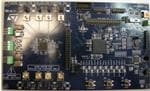
STEVAL-IME003V1
STHV748 Ultrasound Pulser IC evaluation board
Data brief
Description
The STEVAL-IME003V1 evaluation board is
designed around the STHV748 4-channel high
voltage pulser, a state-of-the-art device designed
for ultrasound imaging applications. The output
waveforms can be displayed directly on an
oscilloscope by connecting the scope probe to
the relative BNCs. 16 preset waveforms are
available to test the HV pulser under varying
conditions.
Features
4-channel outputs: high voltage and low
voltage BNC connectors
Load simulator using signal equivalent
circuits
Possibility to set up own load simulator
16 preset waveforms
USB connector to connect STM32 with PC
and supply power to it
4 MB serial Flash memory to host FPGA
code and waveforms
Memory expansion connector to add
external serial Flash
Connectors to supply high voltage and low
voltage to the STHV748 output stage
LEDs to monitor the power management
stage
Human machine interface to select, start and
stop the generation of the preset waveforms
25 LEDs to monitor board behavior
RoHS compliant
August 2015
DocID022109 Rev 2
For further information contact your local STMicroelectronics sales
office
1/12
www.st.com
�Schematic diagram
1
STEVAL-IME003V1
Schematic diagram
Figure 1: STEVAL-IME003V1 hierarchical blocks
2/12
DocID022109 Rev 2
�STEVAL-IME003V1
Schematic diagram
Figure 2: STEVAL-IME003V1 FPGA bank 0 configuration
+
3V3
-
DocID022109 Rev 2
3/12
�Schematic diagram
STEVAL-IME003V1
Figure 3: STEVAL-IME003V1 FPGA bank 1 configuration
4/12
DocID022109 Rev 2
�STEVAL-IME003V1
Schematic diagram
Figure 4: STEVAL-IME003V1 FPGA bank 2 configuration
DocID022109 Rev 2
5/12
�6/12
DocID022109 Rev 2
MCU_FPGA_GPIO0
MCU_FPGA_GPIO1
MCU_FPGA_GPIO2
MCU_FPGA_GPIO3
MCU_FPGA_GPIO4
MCU_FPGA_GPIO5
MCU_FPGA_GPIO6
MCU_FPGA_GPIO7
XC6SLX16-2CSG324C
T15
R15
V16
U16
T13
R13
V15
U15
V14
T14
P12
N12
V13
U13
N11
M11
T11
R11
V12
T12
P11
N10
N9
M10
V11
U11
T10
R10
V10
U10
T8
R8
V9
T9
N8
M8
V8
U8
V7
U7
P8
N7
V6
T6
T7
R7
P7
N6
T5
R5
V5
U5
T3
R3
V4
T4
P6
N5
V3
U3
TP2
TEST POINT
MCU_FPGA_GPIO[0:7]
PROG_LED14
PROG_LED15
MCU_FPGA_GPIO6
MCU_FPGA_GPIO7
MCU_FPGA_GPIO4
MCU_FPGA_GPIO5
PROG_LED12
PROG_LED13
MCU_FPGA_GPIO2
MCU_FPGA_GPIO3
MCU_FPGA_GPIO0
MCU_FPGA_GPIO1
PROG_LED10
PROG_LED11
PROG_LED2
PROG_LED3
PROG_LED6
PROG_LED7
PROG_LED0
PROG_LED1
PROG_LED4
PROG_LED5
PROG_LED8
PROG_LED9
FPGA_SPI_SEL
FPGA_INIT_B
FPGA_MODE1
FPGA_SPI_MISO3
FPGA_SPI_MISO2
FPGA_SPI_MOSI
FPGA_SPI_MISO1
FPGA_MODE0
CCLK
MCU_FPGA_GPIO[0:7]
IO_2_L01N_M0_CMPMISO
IO_2_L01P_CCLK
IO_2_L02N_CMPMOSI
IO_2_L02P_CMPCLK
IO_2_L03N_MOSI_CSI_B_MISO0
IO_2_L03P_D0_DIN_MISO_MISO1
IO_2_L05N
IO_2_L05P
IO_2_L12N_D2_MISO3
IO_2_L12P_D1_MISO2
IO_2_L13N_D10
IO_2_L13P_M1
IO_2_L14N_D12
IO_2_L14P_D11
IO_2_L15N
IO_2_L15P
IO_2_L16N_VREF
IO_2_L16P
IO_2_L19N
IO_2_L19P
IO_2_L20N
IO_2_L20P
IO_2_L22N
IO_2_L22P
IO_2_L23N
IO_2_L23P
IO_2_L29N_GCLK2
IO_2_L29P_GCLK3
IO_2_L30N_GCLK0_USERCCLK
IO_2_L30P_GCLK1_D13
IO_2_L31N_GCLK30_D15
IO_2_L31P_GCLK31_D14
IO_2_L32N_GCLK28
IO_2_L32P_GCLK29
IO_2_L40N
IO_2_L40P
IO_2_L41N_VREF
IO_2_L41P
IO_2_L43N
IO_2_L43P
IO_2_L44N
IO_2_L44P
IO_2_L45N
IO_2_L45P
IO_2_L46N
IO_2_L46P
IO_2_L47N
IO_2_L47P
IO_2_L48N_RDWR_B_VREF
IO_2_L48P_D7
IO_2_L49N_D4
IO_2_L49P_D3
IO_2_L62N_D6
IO_2_L62P_D5
IO_2_L63N
IO_2_L63P
IO_2_L64N_D9
IO_2_L64P_D8
IO_2_L65N_CSO_B
IO_2_L65P_INIT_B
FPGA - Bank 2
1
U4C
R21
2K43 0402DNP
R17
2K43 0402
R22
2K43 0402
MCU_FPGA_MODE1
MCU_FPGA_INIT_B
R18
2K43 0402DNP
1
2
3
4
5
6
7
8
9
10
Place D29
close to J10
EXT SPI
FLASH
CON10 R127
56
J10
R38
GREEN
C33 Details:
TDK (C2012X7R1A106K) - DIGIKEY (445-6857-2-ND)
Dimension 0805 - EIA 2012
C34
100nF
R40
NA 0402
R39
NA 0402
FPGA_SPI_CCLK
FPGA_SPI_MISO1
FPGA_SPI_MOSI
FPGA_SPI_SEL
FPGA_SPI_MISO2
FPGA_SPI_MISO3
MCU_FPGA_PROG
+VFPGA_IO_3V3
C33
10uF 10V 0805
33R2 0402
TO CORRECT
D29
CCLK
FPGA_SPI_MISO1
FPGA_SPI_MOSI
FPGA_SPI_SEL
FPGA_SPI_MISO2
FPGA_SPI_MISO3
Place R38 close to the FPGA device
SPI FLASH CTRL SIGNALS
When FPGA_INIT_B (bidirectional open-drain) is Low the configuration memory
si
being cleared.
When held Low, the start of configuration is delayed
.
During configuration, a Low on this output indicates that a configuration dat
a
error has occurred.
Configuration mode selection:
FPGA_MODE0 = Parallel (Low) or Serial (High
)
FPGA_MODE1 = Master (Low) or Slave (High
)
FPGA_INIT_B
FPGA_MODE0
FPGA_MODE1
R16
10K 0402
+VFPGA_IO_3V3
FPGA CONFIGURATION
PROG_LED7
PROG_LED6
PROG_LED5
PROG_LED4
PROG_LED3
PROG_LED2
PROG_LED1
PROG_LED0
68R 0402
R33
68R 0402
R31
68R 0402
R29
68R 0402
R27
68R 0402
R25
68R 0402
R23
68R 0402
R19
68R 0402
R14
YELLOW
D20
PROG7
YELLOW
D18
PROG6
YELLOW
D16
PROG5
YELLOW
D14
PROG4
YELLOW
D12
PROG3
YELLOW
D10
PROG2
YELLOW
D8
PROG1
YELLOW
D6
PROG0
68R 0402
R34
68R 0402
R32
68R 0402
R30
68R 0402
R28
68R 0402
R26
68R 0402
R24
68R 0402
R20
68R 0402
R15
Kingbright KP-3216SYC
RS: 466-3942
LED 0805
PROG_LED15
PROG_LED14
PROG_LED13
PROG_LED12
PROG_LED11
PROG_LED10
PROG_LED9
PROG_LED8
YELLOW
D21
PROG 15
YELLOW
D19
PROG 14
YELLOW
D17
PROG 13
YELLOW
D15
PROG 12
YELLOW
D13
PROG 11
YELLOW
D11
PROG 10
YELLOW
D9
PROG9
YELLOW
D7
PROG8
Schematic diagram
Figure 5: STEVAL-IME003V1 FPGA configuration
STEVAL-IME003V1
SPI EXTERNAL PROGRAMMING HEADER
AM010069v1
�STEVAL-IME003V1
Schematic diagram
Figure 6: STEVAL-IME003V1 FPGA bank 3 configuration
DocID022109 Rev 2
7/12
�Schematic diagram
STEVAL-IME003V1
Figure 7: STEVAL-IME003V1 FPGA power and configuration
8/12
DocID022109 Rev 2
�DocID022109 Rev 2
THSD_EN
THSD_EN
IN4
IN3D
IN2D
IN1D
IN3C
IN2C
IN1C
IN3B
IN2B
IN1B
N/A
R60
N/A
C110
220n
C104
220n
C100
220n
C94
100
R61
HVM1
HVM0
HVP0
HVP1
HVP0
IN3_A
VDDP
IN3_B
IN2_A
IN1_A
IN2_B
IN1_B
IN4
17
24
23
22
21
20
VDDP
2
19
2
D37
D36
LVOUT_C
1
1
1
DFLS1200
33
34
35
36
37
38
39
40
41
42
43
44
45
46
47
B2S J34
B2S J32
B2S J28
2
2
2
XDCR_C
IN3C
IN2C
IN1C
1
STHV748
AGND
RefHVM1
HVM1_C
HVM0_C
HVOUT_C
HVP0_C
DFLS1200
31
HVM0
BNC
J30
HVP0
1
2
J29
HVP0
DFLS1200
HVM0
DFLS1200
HVP1_C
HVP1_D
RefHVP1
32
D38
GNDPW
27
D35
VDDM
C114 20p 0805
XDCR_B
1
LVOUT_B
LVOUT_B
GNDPW
26
1
XDCR_A
29
J33
LVOUT_C
30
B2S
2
LVOUT_A
BNC
LVOUT_D
VDDM
1
XDCR_C
28
J31
GNDPW
B2S
2
XDCR_D
1
VDDM
J27
HVP0_D
RefHVP0
J23
BNC
220n
C83
3.9n
C107
22n
C99
22n
C93
3.9n
C85
BNC
J26
2
B2S
2
GNDPW
C109
220n
IN3_C
C108
220n
VDDP
IN2B
IN2_C
IN3B
IN3_D
IN1B
IN4
D_CTRL
RefHVM0
HVM1_B
HVM0_B
HVOUT_B
HVP0_B
RefHVP0
HVP1_B
HVP1_A
RefHVP1
HVP0A
HVOUT_D
HVM0_D
HVM1_D
1
C75
HVM1
HVM0
C115 20p 0805
100
R62
THSD
C112
220n
C105
220n
C101
220n
C95
220n
C89
C113
N/A
220n
C103
220n
C97
220n
C91
220n
C87
N/A
R59
100k
R58
10k
THSD_EN
DVDD
J16, J17, J22, J23, J25, J26, J29 and J30 Detail
s
Tyco Electronics (1-1337482-0) - RS (420-5401
)
R63
N/A
N/A
R56
1
2
3
CON3
J24
THSD
C77, C80, C111, C112 Details
DigiKey (490-1462-2-ND) Murata (GRM188R72A271KA01D
)
J16, J17, J22, J23, J25, J26, J29 and J30 Detail
s
Tyco Electronics (1-1337482-0) - RS (420-5401
)
D1, D2, D3 ,D4, D5, D6, D7, D8
diode DFLS1200 rs-code 708-232
4
C80
270p 100V 0603 C81
270p 100V 0603
HVP0
HVP1
HVP0
HVM0
HVM1
R55
100
20p 0805
TP3
TESTPOINT
STHV74 8
48
DVDD
IN1D
IN2D
DGND
2
2
2
XDCR_D
B2S J21
B2S J19
B2S J15
IN3D
1
1
1
RefHVM0
THSD
XDCR_B
16
15
14
13
12
11
10
9
8
7
6
HVOUT_A
220n
IN1_C
BNC
J25
1
3.9n
C106
22n
C98
22n
C92
5
C79
LVOUT_D
IN2_D
1
C111
270p 100V 0603
220n
C102
220n
C96
220n
C90
2
IN4
IN3D
IN2D
IN1D
IN3C
IN2C
IN1C
IN3B
IN2B
220n
HVM0_A
EN
IN1B
IN3A
SUB
4
65
HVM0
64
220n
63
IN1_D
IN3A
C88
62
IN2A
61
HVM1_A
60
3
59
IN2A
HVM1
58
IN1A
57
RefHVM1
56
AGND
55
2
54
1
1
53
3.9n
HVM0
R57
10k
C78
220n
BNC
1
52
C84
U8
DVDD
IN1A
IN2A
IN3A
J20
1
LVOUT_A
51
DVDD
IN1A
C86
220n
C82
XDCR_A
B2S
J18
1
50
HVM0
HVM1
R54
100
B2S
2
J14
DFLS1200
DFLS1200
49
HVM0
HVM1
DVDD
VDDP
VDDM
C77
270p 100V 0603
1
B2S
2
J17
BNC
D34
D32
VDDP
DVDD
VDDP
VDDM
HVP0
HVP1
C76
N/A
J22
BNC
20p 0805
J16
HVP0
HVM0
2
HVP0
HVP1
R53
N/A
C74
1
2
HVM0
DFLS1200
HVP0
DFLS1200
VDDM
2
D33
2
D31
STEVAL-IME003V1
Figure 8: STEVAL-IME003V1 configuration of the STHV748
Schematic diagram
25
18
AM010050v1
9/12
�Schematic diagram
STEVAL-IME003V1
Figure 9: STEVAL-IME003V1 configuration of the STM32
10/12
DocID022109 Rev 2
�STEVAL-IME003V1
2
Revision history
Revision history
Table 1: Document revision history
Date
Version
Changes
11-Aug-2011
1
Initial release.
07-Aug-2015
2
Updated title on the cover page.
DocID022109 Rev 2
11/12
�STEVAL-IME003V1
IMPORTANT NOTICE – PLEASE READ CAREFULLY
STMicroelectronics NV and its subsidiaries (“ST”) reserve the right to make changes, corrections, enhancements, modifications, and
improvements to ST products and/or to this document at any time without notice. Purchasers should obtain the latest relevant information on ST
products before placing orders. ST products are sold pursuant to ST’s terms and conditions of sale in place at the time of order
acknowledgement.
Purchasers are solely responsible for the choice, selection, and use of ST products and ST assumes no liability for application assistance or the
design of Purchasers’ products.
No license, express or implied, to any intellectual property right is granted by ST herein.
Resale of ST products with provisions different from the information set forth herein shall void any warranty granted by ST for such product.
ST and the ST logo are trademarks of ST. All other product or service names are the property of their respective owners.
Information in this document supersedes and replaces information previously supplied in any prior versions of this document.
© 2015 STMicroelectronics – All rights reserved
12/12
DocID022109 Rev 2
�
很抱歉,暂时无法提供与“STEVAL-IME003V1”相匹配的价格&库存,您可以联系我们找货
免费人工找货- 国内价格
- 1+5706.08280
- 200+2276.76960
- 500+2200.68360
- 1000+2163.08880