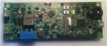
STEVAL-IPP003V1
General purpose xPSK power line communication module
Data brief
Description
The STEVAL-IPP003V1 evaluation board is a
PLM communication module that can be used for
a large set of applications, including metering,
building automation and street lighting. The
module is optimized to operate in CENELEC
bands, but can also work in FCC and ARIP bands
up to 250 kHz with a few modifications.
The module is based on the STM32F103RFT6
ARM Cortex-M3 microcontroller and the ST7580
xPSK narrow band power line modem with up to
28.8 kbps data rate. The MCU mounted on the
board can be easily replaced with an equivalent
64-pin MCU from the STM32F2 or STM32F4
family by a few modification in the assembly. The
module can be coupled to both AC and DC power
line buses and also includes a USB interface for
optional PC connection.
Features
• Insulation from the high voltage mains
•
Interfaces included:
– USB interface
– Dual DC power supply
– Digital interface
– DC or AC insulated bus interface
•
xPSK modulation with bitrate up to 28.8 kbps
• RoHS compliant
December 2013
DocID025671 Rev 1
For further information contact your local STMicroelectronics sales office.
1/7
www.st.com
�Schematic diagram
1
STEVAL-IPP003V1
Schematic diagram
Figure 1. Power supply
CN1
1
2
3
Screw Connector 3P 2.5mm
J7
1
2
3
CON3
VCC
5
1
C1
100nF/25V - 0402
U1
R1
100K - 0603
JP1
OPEN
3
IN
OUT
SHDN
BYPASS
2
C4
100nF/25V - 0402 GND
LK112SM33TR
VCC
VDDIO
4
C2
C3
100nF/25V - 0402
10u/6.3V - 0603
GSPG06112013DI1025
Figure 2. ST7580 reset button (micro-switch)
SW 1
1
2
C17
RESETN
100nF/25V - 0402
GSPG06112013DI1030
Figure 3. ST7580 UART interface
TP8
TXD
1
1
TP9
T_REQ
TXD
T_REQ
1
GND
2/7
DocID025671 Rev 1
RXD
1
TP11
TP12
RXD
GSPG06112013DI1035
�STEVAL-IPP003V1
Schematic diagram
Figure 4. DC BUS / AC BUS
OUTPUT(+)
BUS(+)
OUTPUT(-)
BUS(-)
GSPG06112013DI1040
Figure 5. Current limit setting
1
TP5
CL
R19
VDDIO
330 - 0402
4
CL
2
R21
10k - 0603
Q1
STN4NF06L
R 23
C21
1
130 - 0402
100pF/C0G - 0402
CL_SEL
3
GSPG06112013DI1045
Figure 6. Microcontroller connection
VDDIO
R33
R34
R35
4k7 - 0402
4k7 - 0402
4k7 - 0402
4k7 - 0402
4k7 - 0402
R32
4k7 - 0402
4k7 - 0402
R29
4k7 - 0402
4k7 - 0402
R28
4k7 - 0402
R31
R27
R30
R26
BR0
1
2GPIO_P1
GPIO_BR0
JP2
CLOSE
JP3
CLOSE
RX_ON
1
DFU_FORCE
1 JP4
CLOSE
2
1
JP5
CLOSE
NC_1
nIND
2
JP6
CLOSE
NC_2
1
BR1
TXD
T_REQ
RXD
RESETN
1
2GPIO_P2
2GPIO_P4
2
JP7
CLOSE
JP8
CLOSE
JP9
CLOSE
1
2
1
2
1
2
JP10 CLOSE
TX_ON
1
2
JP11 CLOSE
GPIO_BR1
GPIO_RX
MOSI0_TXD_ST7580
T_REQ_ST7580
MISO0_RXD_ST7580
RESETN_ST7580
GPIO_TX
GSPG06112013DI1050
DocID025671 Rev 1
3/7
7
�ZC_IN
TP15
0 - 0603
R36
XIN
100 nF - 0603
C32
Isolated Zero Crossing
10M - 0402
R40
10M - 0402 (N.A.)
R38
C19
VSSA
47k - 0603
R41
XOUT
XIN
1
TXD
2
RXD
3
VDDIO
R25
4
TRSTN
5
TMS
10k - 0402
GND_SIGNAL 6
7
TCK
8
TDO
9
TDI
10
RESETN
11
VDD
12
XIN
R39
100k - 1206
33k - 1206
R42
33k - 1206
R37
1
2
33k - 1206
R43
STTH1L06A
D5
U2
PA
10k - 0402
R12 R13
C13
100 pF/C0G - 0402
PA_IN+
33k - 0402
TP1
PA_IN-
R16 10k - 0402
R18
10k - 040210k - 0402
10k - 0402
R15
TXD
RXD
VDDIO
TRSTN
TMS
GND
TCK
TDO
TDI
RESETN
VDD
XIN
10k - 0402
C26
C27
C28
100nF/25V - 0402 100nF/25V - 1004u0F2/10V - 0805
TP13
VCCA
10k - 0402
R24
100nF/25V - 0402
Y1
8MHz (N.A.)
C20
VDDIO
10u/6.3V - 0603
VDDIO
R14
100nF/25V - 0402
C15
1nF/C0G - 0402
47k - 0402
22k - 0402
5k1 - 0402
C12
R8
PA_IN-
1
R3
OUTPUT(-)
OUTPUT(+)
PA_OUT
4.7pF/C0G - 0402
100pF/C0G - 0402
C7
C5
TP2
PA_IN+
100nF/C0G - 0402
C8
10k - 0402
R2
27pF/C0G - 0402
C6
R7
R11
1.5k - 0402
R6
47k - 0402
R5
TP7
VDDIO
VCC
C25
100nF/25V - 0402
VDDIO
VCCA
TP10
VDD
VDDIO
ISO1
C11
100nF/25V - 0402
C18
100nF/25V - 0402
TLP781(GP)
TX_OUT
Remove R36 and C28 in DC application
ZC_IN
1
TX_OUT
TP3
To mount only for DC line
VDDIO
VDDIO
4
3
VCC
1
CL_SEL
VSSA
VDDIO
GND
NC#32/DFU_FORCE
STarGRID RESERVED0/P7
NC#30/P8
NC#29/nIND
VDDIO
VDD_REG_1V8
PA_OUT
VSS
R9
C16
18n/25V - 0603
D4
SMAJ5.0CA
150 - 0603
R10
VDD_PLL
VCC
VSS
C33
100nF/25V - 0603
TP16
VCC
100pF/C0G - 0402
VSSA
100nF/25V - 0402
C30
TP14
VDD_PLL
C29
VDD_REG_1V8
TX_ON
RX_ON
DL1
1
SEC
100nF/25V - 0603
C34
C35
47uF/25V - 1210
1
4
J2
1
T1
8
5
OPEN
2
PRI
OPEN
2
R22
0 - 0603
LED-RED
2
R20
LED-GREEN
2
R17
1
J3
560R
CL_ADC
VDDIO
560R
D2
SM6T15CA
15uH - EPCOS B82464-A4153K
L1
TDK SRW 13EP-X07S002 / W E 750-510-231
10u/6.3V - 0603
C24
CL
DL2
1
4.7u/4V - 0402
C31
C23
100nF/25V - 0402
100nF/25V - 0402
C22
BLM21PG331SN1
FB1
nIND
VDDIO
VDD_REG_1V8
PA_OUT
VSS
BLM21PG331SN1
L2
D3
STPS1L30A
10uF/50V X5R 1206
C9
D1
STPS1L30A
220uH - EPCOS B82462-A4224K
10nF/C0G
C14
CL_SEL
VSSA
VDDIO
GND_SIGNAL
DFU_FORCE
P7
TP6
RX_IN
FB2
VCC
24k 1% - 0402
GROUND PLANE
BELOW THE DEVICE
VDD
R4
24k 1% - 0402
VCC
It is recommended to use the specified capacitor dielectrics
(C0G and X7R) to guarantee low distortion
VSSA VSS
36
35
34
33
32
31
30
29
28
27
26
25
RX_IN
TP4
PA_OUT
1
1
2
1
2
VCC
1
2
EXT_XIN
1
1
P7
1
1
48
47
46
45
44
43
42
41
40
39
38
37
RESERVED5
RESERVED4
VDD
GND
RESERVED3
RESERVED2
RESERVED1
PL_TX_ON/P0
BR0/GPIO1
BR1/P2
T_REQ/P3
PL_RX_ON/P4
XOUT
GND
VSSA
VDD_PLL
VCCA
ZC_IN
RX_IN
TX_OUT
PA_IN+
PA_INCL
VCC
13
XOUT
GND_SIGNAL 14
15
VSSA
VDD_PLL 16
17
VCCA
18
ZC_IN
19
RX_IN
20
TX_OUT
21
PA_IN+
22
PA_IN23
CL
24
VCC
EP
49
DocID025671 Rev 1
1
GND_SIGNAL
1
4/7
RX_ON
T_REQ
BR1
BR0
TX_ON
1
OUTPUT(+)
OUTPUT(-)
220nF X1
C10
SEC
4
1
W E 750-510-231
7
10 T2
OUTPUT(-)
PRI
Schematic diagram
STEVAL-IPP003V1
Figure 7. ST7580 module - PLM
GSPG06112013DI1055
�1
C45
22p - 0402
SMD LEDs
22p - 0402
Y3
8MHz
R55
1M - 0402
C46
R52
R53
R54
C38
10pF
OSC-32-IN
OSC-32-OUT
1
D6 2
D7 2
RED
YELLOW
32.768 Khz
Y2
VCC_3V3
C39
10pF
1
D8 2
GREEN
VDDIO
SW 2
1
3
PC4
SW 4
100nF/25V - 0402
2
2
1
SW 3
C40
VCC_3V3
Micro Switch
C36
100nF/25V - 0402
2
1
Micro Switch
SW 5
R56
10K - 0402
VCC_3V3
PD2
CL_ADC
PA1
USART2_TX
USART2_RX
PA4
PA5
PA6
PA7
MCO
PA9
PA10
STM32_USBSTM32_USB+
JT-TMS
JT-TCK
JT-TDI
13
12
60
0 - 0603
R58
7
5
6
54
14
15
16
17
20
21
22
23
41
42
43
44
45
46
49
50
C37
100nF/25V - 0402
PC3
R45
10k - 0402
VCC_3V3
VCC_3V3
100nF/25V - 0402
C42
C41
C43
100nF/25V - 0402
100nF/25V - 0402
1
3
5
7
9
CON10A
J4
2
4
6
8
10
VDDA
VSSA
BOOT0
NRST
C50
10nF/25V - 0402
remove R? and R? for
STM32F4 or STM32F2
0 - 0603 R59
STM32F103RFT6
PB0/ADC-IN8/TIM3-CH3
PB1/ADC-IN9/TIM3-CH4
PB2/BOOT1
PB3/JTDO
PB4/JTRST
PB5/I2C1-SMBA1
PB6/I2C1-SCL/TIM4-CH1
PB7/I2C1-SDA/TIM4-CH2
PB8/TIM4-CH3
PB9/TIM4-CH4
PB10/I2C2-SCL/USART3-TX
PB11/I2C2-SDA/USART3-RX
PB12/SPI2-NSS/I2C2-SMBA1/USART3-CK/TIM1-BKIN
PB13/SPI2-SCK/USART3-CTS/TIM1-CH1N
PB14/SPI2-MISO/USART3-RTS/TIM1-CH2N
PB15/SPI2-MOSI/TIM1-CH3N
PD0/OSC-IN
PD1/OSC-OUT
PD2/TIM3-ETR
PA0-WKUP/USART2-CTS/ADC_IN0/TIM2-CH1-ETR PC0/ADC-IN10
PC1/ADC-IN11
PA1/USART2-RTS/ADC-IN1/TIM2-CH2
PA2/USART2-TX/ADC-IN2/TIM2-CH3
PC2/ADC-IN12
PA3/USART2-RX/ADC-IN3/TIM2-CH4
PC3/ADC-IN13
PA4/SPI1-NSS/USART2-CK/ADC-IN4
PC4/ADC-IN14
PC5/ADC-IN15
PA5/SPI1-SCK/ADC-IN5
PA6/SPI1-MISO/ADC-IN6/TIM3-CH1
PC6
PA7/SPI1-MOSI/ADC-IN7/TIM3-CH2
PC7
PC8
PA8/USART1-CK/TIM1-CH1/MCO
PA9/USART1-TX/TIM1-CH2
PC9
PA10/USART1-RX/TIM1-CH3
PC10
PA11/USART1-CTS/CAN-RX/USBDM(2)/TIM1-CH4
PC11
PA12/USART1-RTS/CAN-TX/USBDP(2)/TIM1-ETR
PC12
PA13/JTMS-SWDAT
PC13/ANTI-TAMP
PA14/JTCK-SWCLK
PC14/OSC32-IN
PA15/JTDI
PC15/OSC32-OUT
C49
10nF/25V - 0402
R57
C47
C48
10nF/25V - 0402 100K - 0402
100nF/25V - 0402
RESET#
300 - 0402 PC5
300 - 0402 PC6
300 - 0402 PD2
V1
BATTERY HOLDER RS: 430-653 PLUS CR1220 lithium coin cell
U4
VCC_3V3
2
1
R44
10k - 0402
PB0
PB1
PB2
JT-TDO
26
27
28
55
56
57
58
59
61
62
29
30
33
34
35
36
PB5
PB6
PB7
PB8
PB9
PB10
PB11
PB12
PB13
PB14
PB15
PC0
PC1
PC2
PC3
PC4
PC5
PC6
PL_BR0
PL_BR1
PC9
PC10
PL_RST
PL_TX_ON
PL_RX_ON
OSC-32-IN
OSC-32-OUT
8
9
10
11
24
25
37
38
39
40
51
52
53
2
3
4
Male Connector 2x5
Pitch 1.27 mm
SAMTEC FTSH-105-01-F-D-K
JT-TMS
JT-TCK
JT-TDO
JT-TDI
RESET#
R47
R46
R48
4k7 - 04024k7 - 04024k7 - 0402
2
1
2
1
2
1
VCC_3V3
PC10
PC9
PL_RX_ON
PL_BR1
PL_RST
PL_TX_ON
CL_ADC
USART2_RX
MCO
USART2_TX
PA1
PB0
PB1
PB2
PL_BR0
PA4
PA5
PA6
PA7
PA9
PA10
PC0
PC1
PC2
NC_1
GPIO_RX
GPIO_BR1
22R - 0402
R50
T_REQ_ST7580
RESETN_ST7580
GPIO_TX
CL_ADC
MISO0_TXD_ST7580
MCO
1
2
3
4
5
6
7
8
9
10
11
12
VDDIO
DIGITAL_B
J6
1.5K - 0402
R51
MOSI0_RXD_ST7580
NC_2
R49
22R - 0402
Strip-Line
DIGITAL_A
J5
GPIO_BR0
1
2
3
4
5
6
7
8
9
10
11
12
STM32_USB+
STM32_USB-
1
2
3
I/O1#6
VBUS
PB5
PB6
PB7
PB8
PB9
PB10
PB11
PB12
PB13
PB14
PB15
100nF/25V - 0603
C44
6
5
4
STM32_USB_PW R
I/O2#4
USBLC6-2P6
I/O1#1
GND
I/O2#3
U3
Mini-USB
CN2
MINI-USB
BLM21PG600SN1D
FB3
1
2
3
4
5
SH2
SH1
VCC_3V3
1
VBAT
32
48
64
19
VDD1
VDD2
VDD3
VDD4
VSS1
VSS2
VSS3
VSS4
DocID025671 Rev 1
31
47
63
18
STEVAL-IPP003V1
Schematic diagram
Figure 8. ST7580 module - MCU
GSPG06112013DI1100
5/7
7
�Revision history
2
STEVAL-IPP003V1
Revision history
Table 1. Document revision history
6/7
Date
Revision
13-Dec-2013
1
Changes
Initial release.
DocID025671 Rev 1
�STEVAL-IPP003V1
Please Read Carefully:
Information in this document is provided solely in connection with ST products. STMicroelectronics NV and its subsidiaries (“ST”) reserve the
right to make changes, corrections, modifications or improvements, to this document, and the products and services described herein at any
time, without notice.
All ST products are sold pursuant to ST’s terms and conditions of sale.
Purchasers are solely responsible for the choice, selection and use of the ST products and services described herein, and ST assumes no
liability whatsoever relating to the choice, selection or use of the ST products and services described herein.
No license, express or implied, by estoppel or otherwise, to any intellectual property rights is granted under this document. If any part of this
document refers to any third party products or services it shall not be deemed a license grant by ST for the use of such third party products
or services, or any intellectual property contained therein or considered as a warranty covering the use in any manner whatsoever of such
third party products or services or any intellectual property contained therein.
UNLESS OTHERWISE SET FORTH IN ST’S TERMS AND CONDITIONS OF SALE ST DISCLAIMS ANY EXPRESS OR IMPLIED
WARRANTY WITH RESPECT TO THE USE AND/OR SALE OF ST PRODUCTS INCLUDING WITHOUT LIMITATION IMPLIED
WARRANTIES OF MERCHANTABILITY, FITNESS FOR A PARTICULAR PURPOSE (AND THEIR EQUIVALENTS UNDER THE LAWS
OF ANY JURISDICTION), OR INFRINGEMENT OF ANY PATENT, COPYRIGHT OR OTHER INTELLECTUAL PROPERTY RIGHT.
ST PRODUCTS ARE NOT DESIGNED OR AUTHORIZED FOR USE IN: (A) SAFETY CRITICAL APPLICATIONS SUCH AS LIFE
SUPPORTING, ACTIVE IMPLANTED DEVICES OR SYSTEMS WITH PRODUCT FUNCTIONAL SAFETY REQUIREMENTS; (B)
AERONAUTIC APPLICATIONS; (C) AUTOMOTIVE APPLICATIONS OR ENVIRONMENTS, AND/OR (D) AEROSPACE APPLICATIONS
OR ENVIRONMENTS. WHERE ST PRODUCTS ARE NOT DESIGNED FOR SUCH USE, THE PURCHASER SHALL USE PRODUCTS AT
PURCHASER’S SOLE RISK, EVEN IF ST HAS BEEN INFORMED IN WRITING OF SUCH USAGE, UNLESS A PRODUCT IS
EXPRESSLY DESIGNATED BY ST AS BEING INTENDED FOR “AUTOMOTIVE, AUTOMOTIVE SAFETY OR MEDICAL” INDUSTRY
DOMAINS ACCORDING TO ST PRODUCT DESIGN SPECIFICATIONS. PRODUCTS FORMALLY ESCC, QML OR JAN QUALIFIED ARE
DEEMED SUITABLE FOR USE IN AEROSPACE BY THE CORRESPONDING GOVERNMENTAL AGENCY.
Resale of ST products with provisions different from the statements and/or technical features set forth in this document shall immediately void
any warranty granted by ST for the ST product or service described herein and shall not create or extend in any manner whatsoever, any
liability of ST.
ST and the ST logo are trademarks or registered trademarks of ST in various countries.
Information in this document supersedes and replaces all information previously supplied.
The ST logo is a registered trademark of STMicroelectronics. All other names are the property of their respective owners.
© 2013 STMicroelectronics - All rights reserved
STMicroelectronics group of companies
Australia - Belgium - Brazil - Canada - China - Czech Republic - Finland - France - Germany - Hong Kong - India - Israel - Italy - Japan Malaysia - Malta - Morocco - Philippines - Singapore - Spain - Sweden - Switzerland - United Kingdom - United States of America
www.st.com
DocID025671 Rev 1
7/7
7
�
很抱歉,暂时无法提供与“STEVAL-IPP003V1”相匹配的价格&库存,您可以联系我们找货
免费人工找货- 国内价格 香港价格
- 1+1399.748441+181.13483