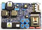
STEVAL-ISA147V3
500 W fully digital AC-DC power supply (D-SMPS) based on
STM32F334C8 microcontroller
Data brief
Description
The STEVAL-ISA147V3 is a digital switch mode
AC-DC converter consisting of two power stages:
an input semi-bridgeless power factor corrector
(SBPFC) controlled by an STM32F051K8, and a
regulation stage implemented with an LLC half
bridge with synchronous rectification (SR),
controlled by an STM32F334C8 microcontroller.
This 500 W AC-DC converter uses the so-called
bridgeless PFC topology, with the advantage of
lower conduction losses and higher efficiency by
eliminating the need for a diode rectifier stage.
This choice also allows a reduced component
count compared to a standard PFC.
Features
Input AC voltage: 90 V to 264 V
Input AC frequency: 45 Hz to 65 Hz
Nominal power: 500 W
Output voltage: 12 V
Semi-Bridgeless PFC stage
DC-DC stage: resonant LLC with
synchronous rectification
Peak efficiency: 94%
PFC switching frequency: 60 kHz
DC-DC switching frequency: 80 kHz to 115
kHz (burst mode above)
HF transformer isolation voltage: 4 kV
Cooling: natural convection up to 300 W,
forced cooling above 300 W
PFC control: managed by STM32F051K8
LLC control: managed by STM32F334C8
Input short-circuit protection
Input under/overvoltage protection
Input under/overfrequency protection
DC Bus under/overvoltage protection
Output short-circuit protection
Output under/overvoltage protection
Overtemperature protection
RoHS compliant
March 2016
The input stage is typically controlled using an
outer voltage loop for bus voltage regulation and
an inner control loop to shape the current
according to a sinusoidal waveform. The outer
loop adjusts the current reference in order to
maintain a regulated bus voltage, independent of
load or input voltage variations. The output
isolation and regulation stage is implemented
using a half-bridge LLC topology, operating with
constant duty cycle and variable frequency
control.
DocID029092 Rev 1
For further information contact your local STMicroelectronics sales
office
1/10
www.st.com
�Description continued
1
STEVAL-ISA147V3
Description continued
The DC-DC stage performs voltage step-down using an HF transformer with a primary to
secondary turn ratio chosen to maintain good efficiency and regulation over the entire
operating range. The transformer is supplied with a square wave voltage generated by the
primary side active switches. On the secondary side, this voltage waveform is rectified and
then smoothed by the output filter; on the primary side, switching losses are reduced
thanks to zero voltage switching (ZVS). On the secondary side, synchronous rectification
(SR) is used to ensure low conduction losses. The overall effect of these design choices is
high system efficiency, in line with the stringent requirements of the power supply industry.
The system is controlled by two microcontrollers from the STM32 product family. On the
primary side, an STM32F051K8 controls the bridgeless PFC by sampling the current of the
two MOSFETs, the input AC voltage and the output bus voltage. Two control signals,
PWM1 and PWM2, are then generated to drive two power switches. On the secondary
side, an STM32F334C8 microcontroller samples the output voltage and adjusts the
frequency of the LLC bridge control signals to ensure stable operation throughout the
overall load range. In addition, two ADC channels are used to sample the rising and falling
edges of the drain-to-source voltage of the SR MOSFETs. The two microcontrollers
exchange information about the status of the input and output power stage via bidirectional
serial communication.
Both the power stage and control stage are supplied by an offline flyback circuit which
provides a suitable, regulated voltage to the microcontrollers, the gate drive ICs and signal
conditioning circuits.
2/10
DocID029092 Rev 1
�F1
FUSE
R3 R4 R6
470K 9241108
470K 9241108
470K 9241108
R27
R31
R36
C21
1uF X2 1781894
C22
1nF
R34
470K 9241108
R30
470K 9241108
R26
470K 9241108
EARTH2
C97
4n7 Y2 1166486
4
2
3.3nF
5K1
R43
8n2
C65
1K
C76
3.3nF
GND1
R41
C83
100nF
GND1
D11
R38
GND1
R32 10K
10K
BAR 43 AS no t conne cted
3
1
ININ+
C53
C12
+3.3 Primary
GND1
4
TSV611
OUT
GND1
R18
nc
GND1
D13
1N4007
U6
GND1
2000
R40
C20
100nF
0
D12
1N4007
PFC VAC
G_PFC1
Q1
2
500uH 10A
L2
1
3
GND1
1
MURATA 53020C
S T P 42N60M2-EP
3
T4
4
R15 22
GND1
R21
6.8
STPS1L309907491
D19
R51
D9
D10
1N4007 1N4007
PFC CS1
GND1
R50
nc
0
G_PFC2
GND1
R22
6.8
STPS1L309907491
D14
R49
D7
STPSC1006D
R16 22
S T P 42N60M2-EP
3
4
500uH 10A
1
3
Q2
MURATA 53020C
T5
GND1
1
2
L1
D8
STPSC1006D
100uF 450V 1166652
C35
100uF 450V 1166652
C14
100uF 450V 1166652
C36
100uF 450V 1166652
GND1
C34
C25
560nF 1890496
C23
+3.3 Primary
560nF 1890496
GND1
+3.3 Primary
C64
C16
560nF 1890496
PFC CS2
1K
GND1
C71
C46
EARTH
4n7 Y2 1166486
C26
L3
1636294
4n7 Y2 1166486
C1
560nF 1890496
R39
EARTH
C18
4n7 Y2 1166486
C24
L6
1636294
4
2
4n7 Y2 1166486
C15
1uF X2 1781894
C96
3
4n7 Y2 1166486
470K 9241108
470K 9241108
3
2
1
Header 3
EARTH2
1uF X2 1781894
JP1
470K 9241108
1
3
1
EARTH
560nF 1890496
2
1
EARTH
560nF 1890496
5
V+
V-
DocID029092 Rev 1
2
1
2
2
1
2
1
C17
560nF 1890496
560nF 1890496
GNDpri
+3.3V pri
- OUT PFC
C19
+ OUT PFC
2
EARTH2
STEVAL-ISA147V3
Schematic diagram
Schematic diagram
Figure 1: STEVAL-ISA147V3 circuit schematic (1 of 6)
GSPG0903151420SG
3/10
�DocID029092 Rev 1
3.3V pri
- OU T PF C
Bridg e curr ent
R77
300
Q12
N.C.
GND pri
+3.3V pri
Bridg e LS_P
D20
100nF
C48
0
R81
C43
20
20
20
C49
100nF
0
10
12
13
ACPL-P484 2070254 U10
U11
Vcc
Vo
U 12
GN D
Vo
V cc
4n7 4kV
C80
PS 9821 /KB357 NT
1
8
7
6
PS 9821 /KB357 N T
5
GN D
1
2
3
4
1
2
5
6
3
4
1
2
6
3
N.C.
Q17
5
ACPL-P484 2070254 U9
D23
2
39 /200 for 357 N T
R86
3
0
R104
4
R84
CapLL C
6
3
15
8
5
6
7
D 36
1N 4148 W 1469425
GND 2
0
GND 2
C50
100nF
GND 2
R44
47
R35
47
GND 2
GD R_2
GND 2
Bridg e LS_P_M CU
nc/820 for 357 NT
U SART1 RX Sec ond ary
R103
Q 14
Bridg e H S_P_M CU
Q10
39
R42
39
USA RT1 TX Sec ond ary
39 /200 for 357 NT
0
0
R85
3.3V sec
R83
R82
R100
300
R80
GND 2
300
R79
GND 2
Q8
STL 220 N6F7
VD rain2
1N4148 W 1469425
R37
1K
T7
TRAN SF ORM ER LP4525-H
GND 2
4
nc/820 for 357 NT
USA RT1 TX Prim ary
3.3V pri
R101
+V cc
+V cc
100nF
C47
1N 4148 W 1469 425 M M SD914
U SART1 RX Prim ary
C44
10u F 2112705
Q4
R74
R52
R56
Q3
Q11
Bridg e H S_P
STP25N60M2-EP
GD _2
OU T
GD _1
15n F 18 54929
STP25N60M2-EP
220p F 1216461
C45
15n F 1854 929
N.C.
C84
D 33
STL 220 N 6F7
+ OU T PF C
1N4148 W 1469425 M M SD914
T2
N.C.
N.C.
Q16
C89
22pF
Q6
STL 220 N6F7
curr ent_cycle
D 37
BAT754
curr ent_AV G
VD rain2
GND 2
3.3V sec
Q7
Discharge
V D rain2
GND sec
300
GD R_1
R97
+3.3V sec ond ary
Q13
VD rain1
STL 220 N6F7
3.3V sec
N.C.
BA T754 R29
1K
R33
150 0uF 16V 155 1414
MAGNETICA 24.340.002
C39
C40
FAN switch
C41
GND 2
C42
+12V
Q9
PM BF170 1081473
R94
100
GND 2
150 0uF 16V 155 1414
C88
10nF
150 0uF 16V 155 1414
C87
3uF
150 0uF 16V 155 1414
D28
C90
330
R111
10u F X 7R 2112722
3.3V sec
C91
C92
C93
Q 15
STN 4NF03L
GND 2
10u F X 7R 2112722
4/10
10u F X 7R 2112722
GND 2
14
12
10
8
6
4
2
P6
13
11
9
7
5
3
1
GND 2
GND 2
Hea der 7X2H 1551388
12V
FAN
1
2
3
P7
0 (nc)
R115
Schematic diagram
Figure 2: STEVAL-ISA147V3 circuit schematic (2 of 6)
STEVAL-ISA147V3
GSPG0903161500SG
10u F X 7R 2112722
�DocID029092 Rev 1
C81
nc
C78
1uF
C85
100pF
R23
0
Bridge HS_P
+Vcc
SD L6491D
C79
100nF
C82
100pF
C31
C29
1
2
3
4
5
6
7
4
1
2
3
LVG
GND
L6491D
LIN
SD/OD
HIN
VCC
DT
SGND
PGND
CP+
CPLVG
BOOT
HVG
OUT
Q5
PMBF170 108147 3
330
R67
10
9
8
14
13
12
R65
nc
R66
300
+3.3 Primary
OUT
HVG
BOOT
4u7
C77
R68
nc
5
6
7
8
L6387E (not mounted)
LIN
HIN
VCC
U7
C32
100pF (not mounted)
U8
R62
10K
Bridge LS_P
100pF (not mounted)
Bridge LS_P
Bridge HS_P
1uF (not mounted)
C72
100nF (not mounted)
+Vcc
+Vcc
OUT
10K
+Vcc
+3.3 Primary
BAT754
D16
BAT754
R20
R25 1K
R59 82
R58 3.3
R55 82
R54 3.3
D15
4u7 (not mounted)
C28
+3.3V pri
SR2
SR1
GND pri
GD_2
OUT
GD_1
R61
R60
GND2
GND2
GND2
330
1
2
3
4
R57 360
10K
R63
330
PFC PWM 1
PFC PWM 2
R53 360
C86
C33
PM8834
ENB1
PWM1
GND
PWM2
IC2
R64 10K
1uF
100nF
ENB2
OUT1
VCC
OUT2
PM8834
8
7
6
5
1uF
+Vcc
G_PFC1
G_PFC2
EN DR PFC
0
0
D17
R118
R117
6V Viper
BAT754
D18
GDR_2
GDR_1
EN SYNC RECT
8
7
6
5
BAT754
ENB2
OUT1
VCC
OUT2
12V
100nF
C73
C30
ENB1
PWM1
GND
PWM2
GND sec
1
2
3
4
IC1
STEVAL-ISA147V3
Figure 3: STEVAL-ISA147V3 circuit schematic (3 of 6)
Schematic diagram
GSPG0903161445SG
5/10
�PFC CS2
SD L6491D
330
PFC CS1
R109
470
+3.3 Primary
R45
C94
47pF
D22
BAT754
C56
1uF
Bridge current
D21
BAT754
+3.3 Primary
C55
100nF
100nF
C51
GND1
U5
LM19CIZ
+3.3 Primary
1
2
+VS
VO
C67
GND
100nF
+3.3 Primary
C95
47pF
330
R108
L4
3
470
R17
I2C1_SDA
I2C1_SCL
U13
DAC out
P2
GND1
Header 4
1
2
3
4
P3
+3.3 Primary
1
2
3
4
PFC PWM 2
GNDpri
+3.3V pri
+ OUT PFC
R96
3K9
R95
180K
C58
10nF
D25
BAT754
R92 +3.3 Primary
180K
R91
180K
USART1 RX Primary
EN DR PFC
P4
Header 4
+3.3 Primary
PFC PWM 1
470
R28
+3.3 Primary
+3.3 Primary
C57
100nF
LED 1058385
D24
24
23
22
21
20
19
18
17
T9
test
Test point
PA14
PA13
PA12
PA11
PA10
PA9
PA8
VDD
620
22nF
C68
1
R93
Test point
STM32F051Kx
VDD
PF0/OSC_in
PF1/OSC_out
NRST
VDDa
PA0
PA1
PA2
+3.3 Primary
C27
100nF
BAT754
D38
+3.3 Primary
1
2
3
C52
4
5
10nF
6
7
8
R87
10K
T8
1
32
31
30
29
28
27
26
25
PB8
BOOT0
PB7
PB6
PB5
PB4
PB3
PA15
PA3
PA4
PA5
PA6
PA7
PB0
PB1
PB2/BOOT1
9
10
11
12
13
14
15
16
DocID029092 Rev 1
PFC VAC
6/10
test
USART1 TX Primary
Schematic diagram
Figure 4: STEVAL-ISA147V3 circuit schematic (4 of 6)
STEVAL-ISA147V3
GSPG0903161515SG
�GSPG0903161540SG
DocID029092 Rev 1
6V Viper
GND2
VCC
GND sec
+3.3V secondary
0
R73
STM32F 334
R72
0
cu rr ent_AVG
R11 3
2k
R11 0
2k
Vb
bat
PC
C 13
PC
C 1 4 / O S C 3 2 in
PC
C 1 5 /O S C 3 2 o u t
PD
D 0 / O S C in
PD
D 1 /O S C o u t
NR
RST
VS
SSa
VDDa
PA0
PA1
PA2
R48
C74
100n F
D32
BAT754
GND2
to main GND2
R69 0
R46 0
R47 0
C54 10n F
GND2 10 K R99
GND2
0
GND2
C9 8
nc (47 to 100 nF)
1
R10 5
1K 0.1%
C66
1nF
D27
BAT754
GND2
1
2
3
4
5
6
7
8
9
10
11
12
C59
100n F
GND2
VCC
GND2
C69
100n F
SR leg1
SR leg2
36
35
34
33
32
31
30
29
28
27
26
25
VCC
R76
R78
R88
R89
R90
0
0
0
0
0
R75 0
GND2
VCC
200
R98
D35
VCC
BAR43S
GND2
D29
VCC
GND2
VC C
BAR43S
GND2
C75
47p F
R11 4
GND2
C70
47p F
R10 7
0
0
USART1 TX Secondary
USART1 RX Sec ondary
R11 2
360
VC C
VDrain1
D34
BAT754
BAT 754
R10 6
360 D30
2
3
4
Header 4
1
2
3
4
Heade r 4
P8
1
VCC
P5
LED 1058385
D26
FAN switch
SR1
Bridg e HS_P_MC U
Bridg e LS_P_MCU
SR 2
GND2
100n F
C60
GND2
EN SYNC RECT
VCC
VDD_3
VSS_3
PA13
PA12
PA11
PA10
PA9
PA8
PB15
PB14
PB13
PB12
U14
470
R19
GND2
24
23
22
21
20
19
18
17
16
15
14
13
12 V
R10 2
VCC
GND2
C3
100n F
20p F
2
VDD_2
VSS_2
PB11
PB10
PB2
PB1
PB0
PA7
PA6
PA5
PA4
PA3
4K3 0.1%
C63
1u F
GND2
Y2
1
C62
8Mhz HC49 /US
T12 T13
Test p oint
1
20p F
C61
Temp SR out
Test p oint
test
test
VCC
R24
470
C38
100n F
GND2
2
PA14
PA15
PB3
PB4
PB5
PB6
PB7
BOOT0
PB8
PB9
VSS_1
48 VDD_1
GND2
VCC
VO
GND2
3
37
38
39
40
41
42
43
44
45
46
47
GND2
L5
GND
+VS
U 15
LM19 CIZ
I2C
3
2
1
GND2
C37
100n F
VCC
1
P9
V Drain2
STEVAL-ISA147V3
Figure 5: STEVAL-ISA147V3 circuit schematic (5 of 6)
Schematic diagram
Temp SR out
Discharge
cu rr ent_cycle
0
R71
0
R70
7/10
�3
Vin
GND
1
Vout
2
GNDpri
C13
100uF 16V 1780615
+3.3V pri
+Vcc
R2
3.3
C10
nc
100uF 25V 1780615
C8
D6
BAR46
-OUT PFC
R12
nc
R11
33K
3
5
R7
180K
CONT
BR
VDD
C11
22nF
FB
CONTROL
D3 STTH1L06
U2
R13
47K
C9
120nF
SOURCE
DRAIN
VIPER 27H N
C4
22uF 35V 1899657
D4
1N4148W 1469425
R1
1
D5
BAR46
D2
7
1.5KE250
8
1
PC817 D
OPTO1
2
4
1
5 TR1
8
6
4
TS431ILT
U3
9
7
Viper transfo WE MIDCOM
4
3
+ OUT PFC
2
4
1
2
3
2
DocID029092 Rev 1
A
K
NC
NC
VREF
2.4K
R5
R10
160K
C7
82nF
R8
1.8K
470uF 16V YXF
R14
4.3K
R9
16K
GND2
C2
GND2
STPS2L40
D1
C5
1uF
3
Vout
Vin
GND
GND2
GND2
1
8/10
5
1
+3.3V secondary
6V Viper
1
2
Header 2
C6
100uF 16V 1780615
4
GNDsec
Vout
2
U1
LD1117
P1
Schematic diagram
Figure 6: STEVAL-ISA147V3 circuit schematic (6 of 6)
STEVAL-ISA147V3
U4
LD1117
GSPG0903161400SG
�STEVAL-ISA147V3
3
Revision history
Revision history
Table 1: Document revision history
Date
Version
Changes
11-Mar-2016
1
Initial release.
DocID029092 Rev 1
9/10
�STEVAL-ISA147V3
IMPORTANT NOTICE – PLEASE READ CAREFULLY
STMicroelectronics NV and its subsidiaries (“ST”) reserve the right to make changes, corrections, enhancements, modifications, and
improvements to ST products and/or to this document at any time without notice. Purchasers should obtain the latest relevant information on ST
products before placing orders. ST products are sold pursuant to ST’s terms and conditions of sale in place at the time of order
acknowledgement.
Purchasers are solely responsible for the choice, selection, and use of ST products and ST assumes no liability for application assistance or the
design of Purchasers’ products.
No license, express or implied, to any intellectual property right is granted by ST herein.
Resale of ST products with provisions different from the information set forth herein shall void any warranty granted by ST for such product.
ST and the ST logo are trademarks of ST. All other product or service names are the property of their respective owners.
Information in this document supersedes and replaces information previously supplied in any prior versions of this document.
© 2016 STMicroelectronics – All rights reserved
10/10
DocID029092 Rev 1
�
很抱歉,暂时无法提供与“STEVAL-ISA147V3”相匹配的价格&库存,您可以联系我们找货
免费人工找货