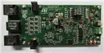
STEVAL-TSP004V2
Data brief
5 V/4 A, synchronous flyback converter, Power Over Ethernet (PoE) - IEEE
802.3at compliant reference design
Features
•
•
•
IEEE 802.3at compliant PD interface
Works with power supplied from Ethernet LAN cables or from local auxiliary
sources
Line input voltage range: 40 to 60 VDC
•
Output voltage: 5 VDC ± 5%
•
•
•
•
•
Output current: 4 A
Peak-to-peak output ripple: < 30 mV
Efficiency DC-DC full-load: > 92%
Overall peak efficiency: > 89%
Transient response ΔVOUTPK-PK to 50% load step: < 170 mV
•
•
ΔV in load line case: < 0.5%
RoHs compliant
Description
The STEVAL-TSP004V2 is a reference design for a PoE+, high-efficiency, 5 V/4 A
flyback converter based on the PM8803 PoE controller.
The PM8803 is a highly integrated device embedding an IEEE802.3at-compliant
powered device (PD) interface together with a PWM controller and support for
auxiliary sources.
Product summary
The STEVAL-TSP004V2 reference design is based on an isolated flyback CCM
converter featuring synchronous rectification with gate driver transformer.
5 V/4 A, synchronous flyback converter, Power
STEVALOver Ethernet (PoE) - IEEE
TSP004V2
802.3at compliant
reference design
High efficiency integrated
IEEE 802.3at PoE-PD
interface and PWM
controller type 2 PSE
indicator, plus support for
forward active clamp
topology
PM8803
DB2569 - Rev 2 - May 2019
For further information contact your local STMicroelectronics sales office.
www.st.com
�STEVAL-TSP004V2
Detailed description
1
Detailed description
The STEVAL-TSP004V2 reference design for the PM8803 covers a broad range of Power over Ethernet (PoE)
applications.
The PM8803 is a highly integrated device embedding an IEEE802.3at-compliant powered device (PD) interface
together with a PWM controller and support for auxiliary sources.
Although the PM8803 can be configured to work in several isolated topologies (self-driven or transformer gatedriven), we focus here on a high-efficiency isolated flyback converter topology with synchronous rectification, 5 V
output voltage and 4 A output current capability.
Auxiliary sources can be connected to the reference design on two different input connectors: one input (AUX II)
allows prevalence of the auxiliary sources with respect to the PoE, whereas the other input (AUX I) allows the use
of a wall adapter with voltage lower than the internal PoE UVLO threshold, while still benefitting from the inherent
inrush and DC current limit.
The possible configurations supported by the STEVAL-TSP004V2 reference design are:
•
input diode bridges (four possible options, including active bridges)
•
optional 4-pair detection circuit to detect a high power PSE source
•
optional booster circuit to increase the max. input current over 800 mA
•
diode or synchronous rectification (four package options for diode and three package options for MOSFET)
•
primary side snubber (three options including active clamp)
•
power transformer (three size options for transformer gate-driven solutions and two size options for selfdriven applications)
1.1
Efficiency
Figure 1. STEVAL-TSP004V2 reference design: 5 VOUT overall and DC-DC efficiency
DB2569 - Rev 2
page 2/5
�STEVAL-TSP004V2
Schematic diagrams
2
Schematic diagrams
Figure 2. STEVAL-TSP004V2 circuit schematic (1 of 2)
Chassis
Chassis
J3
10
10
T1
1
2
3
4
5
6
7
8
12
13
1
2
3
4
5
6
7
8
11
14
10
R175R
15
J4
DATA OUTPUT
9
9
0603
16
9
Chassis
Chassis
17
8
7
Data and power input
R275R
18
0603
6
19
5
20
4
R575R
21
0603
22
3
23
2
1
R10
75R
0603
C5
10nF 10%
0603
100V
R11
75R
0603
R12
75R
0603
R775R
24
0603
ETH1-460
R13
75R
0603
C9
2.2nF
2KV
1812 1206
C8
10nF 10%
0603
100V
C6
C7
10nF 10% 10nF 10%
0603
0603
100V
100V
R1250R0
TP24
BLACK
C12
2.2nF
2KV
1812
Chassis
Chassis
SP
TP22
Red
TP2
Red
AUX 1
J2
D1
R26
1
2
3
0R01206
R17
POE+F
POE+F
0R01206
STTH302S
SMC
SP
C14
1nF 10%
0603
100V
D9
STPS2H100A
SMA
D8
STPS2H100A
SMA
D4
STPS2H100A
SMA
D7
STPS2H100A
SMA
R32
15K
0805
D12
STPS2H100A
SMA
D17
STPS2H100A
SMA
D14
STPS2H100A
SMA
RTN
C18
D11
0.1µF 10% SMAJ58A
SMA
0805
100V
C16
1nF 10%
0805
100V
C21
1nF 10%
0603
100V
D13
STPS2H100A
SMA
R37
R43
0R0 1206
0R01206
TP3
BLACK
Auxiliary input frontal or AUXI
VSS
TP23
BLACK
Figure 3. STEVAL-TSP004V2 circuit schematic (2 of 2)
48VAUX2
J1
TP7
Red
TP4
Red
R49
1206
0R0
1
2
3
D21
L5
TP9
Red
10µH
1
STTH302S
C22
TBD
2
MSS7341-103ML
2KV
1812
SMC
SA
C64
R51
15K
0805
2.2µ
1210
100V
C26
33µF 20%
100V
10x10.2
C28
C29
2.2µ
1210
100V
2.2µ
1210
100V
C30
68pF
0805
100V
TP5
Red
R23
100R
1206
R54
1206
0R0
L60.33uH
7
6
1
1
Red
2
9
10
1206
8
7
6
5
4
T5
5
D28
R66
10R
D52
BAT46J
R70
10K 1%
1%
10nF
R65
1K
C67
C68
22uF
1206
16V
22uF
1206
16V
22uF
1206
16V
22uF
1206
16V
4
C33
C35
22uF
1206
16V
22uF
1206
16V
C34
330uF
16V
8x10.2
1
2
D26
C36
0.1u
1
2
TP12
BLACK
Output filter
STL60N3LLH5
TP13
Red
10R
BAT46J
C39
1uF
25V
0603
SOD323
C37
PowerFLAT™ 5x6
R62
C38
3
2
1
C27
Q12
COILCRAFT HA3691-AL
R58
27K
J5
R52
3K3
0805
0805
TP10
Red
SA
R53
5R
Out det
C31
1.5nF
R21
220R
RTN
POE+F
R72
120K 1%
1%
TP6
2
DO1813-331ML
Input filter
TP8
BLACK
SOD323
TP14
Red
C41
1uF
25V
0603
D32
MM3Z15VT1
SOD323
C40
1uF
25V
0805
RTN
D34
COILCRAFT DA2319-AL
R64
0R0
4
ARTN
R84
R131
R27
SP
15
30R9 1%
R0805
14
R95
27k
13
24.9K 1%1%
12
11
C19
10nF
VSS
MMBT3904LT1
SOT23
Q18
R38
1k
C69
10nF
R101
24.9K 1%
1%
R9
1K 1%
R0603
FRS
RTN
GAT1
CLS
VC
SP
GAT2
DET
ARTN
VDD
RTN
VDD
PM8803
C23
470nF 10%
50V
0603
VB
CS
DT
SA
DCCL
VSS
D36
BAT46J
SOD323
Q16
MMBT3906LT1
SOT23
1
0R0
R96
0R0
U3
2
R89
3.3K
3
4
R92
10R
5
TP16
6
TP15
Red
D57
7
BAT46J
8
2
C49
3.3nF
C50
47nF
SO8
4
Q17
BAT46J
ARTN
D40
SOD323
TP18
Red
R107
10K
R1044.7K 1%
C5647nF
BAT46J
HTSSOP20-LARGE
ARTN
C55
100pF
R99
47K
D39
510R
C54
470p
C60
1nF
C59
1µF
25V
0603
R108
R109
0.30 ohm 1% 0.30 ohm 1%
1206
1206
0805
Power circuit
VC
TP19
BLACK
RTN
C61
2.2n
2KV
1%
SOD323
3
100V
TP11
BLACK
C48
1µF
25V
0603
R93
1K
R94
21K 1%
1%
Si4848DY
9
C53
1uF
1
SOD323
R103
10
4
3
R90
1k5
Red
R0805
R91
10R
Fairchild FOD817AS
0.1uF
5
6
7
8
17
16
CTL
R83
10K
3
R80
20R
T8
1
2
3
19
18
T2P
ExPad
20
BAT46J
SOD323
0.1uF
C45
21
T2P
6
RTN
U1
C44
1
U4
4
1
2
TS431AILT
R111
12.4K 1%
1%
R112
15K 1%
1%
5
SOT23-5
1812
RTN
Feedback circuit
ARTN
R122
0R0
RTN
D20
Aux det
SA
SP
JM1
Double jumper
U2
R45
1
2
3
JM2
Double jumper
VSS
3
24.9K
Fairchild FOD817AS
1
4
2
3
R44
3K3
D44
T2P det
TP21
Red
Auxiliary present
U7
R1175.1K
VC
T2P
Fairchild FOD817AS
1
4
2
3
R119
3.3K
TP20
Red
T2P present
1
2
RTN
DB2569 - Rev 2
page 3/5
�STEVAL-TSP004V2
Revision history
Table 1. Document revision history
Date
Version
24-Apr-2015
1
Changes
Initial release.
Updated title.
07-May-2019
2
Added product summary table.
Minor text and formatting changes.
DB2569 - Rev 2
page 4/5
�STEVAL-TSP004V2
IMPORTANT NOTICE – PLEASE READ CAREFULLY
STMicroelectronics NV and its subsidiaries (“ST”) reserve the right to make changes, corrections, enhancements, modifications, and improvements to ST
products and/or to this document at any time without notice. Purchasers should obtain the latest relevant information on ST products before placing orders. ST
products are sold pursuant to ST’s terms and conditions of sale in place at the time of order acknowledgement.
Purchasers are solely responsible for the choice, selection, and use of ST products and ST assumes no liability for application assistance or the design of
Purchasers’ products.
No license, express or implied, to any intellectual property right is granted by ST herein.
Resale of ST products with provisions different from the information set forth herein shall void any warranty granted by ST for such product.
ST and the ST logo are trademarks of ST. For additional information about ST trademarks, please refer to www.st.com/trademarks. All other product or service
names are the property of their respective owners.
Information in this document supersedes and replaces information previously supplied in any prior versions of this document.
© 2019 STMicroelectronics – All rights reserved
DB2569 - Rev 2
page 5/5
�
很抱歉,暂时无法提供与“STEVAL-TSP004V2”相匹配的价格&库存,您可以联系我们找货
免费人工找货- 国内价格 香港价格
- 1+1397.386891+173.89012
- 国内价格
- 1+2905.29720
- 200+1159.23960
- 500+1120.50000
- 1000+1101.35160


 工商网监
湘ICP备2023018690号
工商网监
湘ICP备2023018690号
