STF26N60DM6
Datasheet
N-channel 600 V, 165 mΩ typ., 18 A, MDmesh DM6 Power MOSFET
in a TO‑220FP package
Features
1
2
3
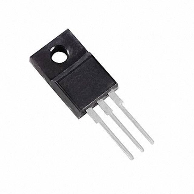
TO-220FP
D(2)
G(1)
Order code
VDS
RDS(on) max.
ID
STF26N60DM6
600 V
195 mΩ
18 A
•
•
Fast-recovery body diode
Lower RDS(on) per area vs previous generation
•
•
•
•
Low gate charge, input capacitance and resistance
100% avalanche tested
Extremely high dv/dt ruggedness
Zener-protected
Applications
•
S(3)
AM15572v1_no_tab
Switching applications
Description
This high-voltage N-channel Power MOSFET is part of the MDmesh DM6 fastrecovery diode series. Compared with the previous MDmesh fast generation, DM6
combines very low recovery charge (Qrr), recovery time (trr) and excellent
improvement in RDS(on) per area with one of the most effective switching behaviors
available in the market for the most demanding high-efficiency bridge topologies and
ZVS phase-shift converters.
Product status link
STF26N60DM6
Product summary
Order code
STF26N60DM6
Marking
26N60DM6
Package
TO-220FP
Packing
Tube
DS12863 - Rev 2 - September 2020
For further information contact your local STMicroelectronics sales office.
www.st.com
�STF26N60DM6
Electrical ratings
1
Electrical ratings
Table 1. Absolute maximum ratings
Symbol
Value
Unit
Gate-source voltage
±25
V
Drain current (continuous) at TC = 25 °C
18
A
Drain current (continuous) at TC = 100 °C
11
A
Drain current (pulsed)
60
A
Total power dissipation at TC = 25 °C
30
W
dv/dt(2)
Peak diode recovery voltage slope
100
V/ns
di/dt(2)
Peak diode recovery current slope
1000
A/µs
dv/dt(3)
MOSFET dv/dt ruggedness
100
V/ns
VISO
Insulation withstand voltage (RMS) from all three leads to external heat sink
(t = 1 s, TC = 25 °C)
2.5
kV
Tstg
Storage temperature range
-55 to 150
°C
Value
Unit
4.17
°C/W
50
°C/W
Value
Unit
VGS
ID
IDM
(1)
PTOT
Tj
Parameter
Operating junction temperature range
1. Pulse width is limited by safe operating area.
2. ISD ≤ 18 A, VDS (peak) < V(BR)DSS, VDD = 400 V.
3. VDS ≤ 480 V
Table 2. Thermal data
Symbol
Rthj-case
Rthj-amb(1)
Parameter
Thermal resistance junction-case
Thermal resistance junction-ambient
1. When mounted on FR-4 board of inch², 2oz Cu.
Table 3. Avalanche characteristics
Symbol
DS12863 - Rev 2
Parameter
IAR
Avalanche current, repetitive or not repetitive (pulse width limited by Tjmax)
4
A
EAS
Single pulse avalanche energy (starting TJ = 25 °C, ID = IAR, VDD = 50 V)
360
mJ
page 2/12
�STF26N60DM6
Electrical characteristics
2
Electrical characteristics
TC = 25 °C unless otherwise specified
Table 4. On/off states
Symbol
V(BR)DSS
Parameter
Test conditions
Drain-source breakdown voltage
VGS = 0 V, ID = 1 mA
Min.
Typ.
600
Zero gate voltage drain current
1
µA
100
µA
±5
µA
4
4.75
V
165
195
mΩ
Min.
Typ.
Max.
Unit
-
940
-
pF
-
75
-
pF
-
4
-
pF
VGS = 0 V, VDS = 600 V,
TC = 125 °C(1)
IGSS
Gate-body leakage current
VDS = 0 V, VGS = ±25 V
VGS(th)
Gate threshold voltage
VDS = VGS, ID = 250 µA
RDS(on)
Static drain-source on-resistance
VGS = 10 V, ID = 9 A
Unit
V
VGS = 0 V, VDS = 600 V
IDSS
Max.
3.25
1. Defined by design, not subject to production test.
Table 5. Dynamic
Symbol
Parameter
Ciss
Input capacitance
Coss
Output capacitance
Crss
Reverse transfer capacitance
(1)
Test conditions
VDS = 100 V, f = 1 MHz,
VGS = 0 V
Equivalent output capacitance
VDS = 0 to 480 V, VGS = 0 V
-
157
-
pF
RG
Intrinsic gate resistance
f = 1 MHz, ID = 0 A
-
4.8
-
Ω
Qg
Total gate charge
VDD = 480 V, ID = 18 A,
-
24
-
nC
Qgs
Gate-source charge
VGS = 0 to 10 V
-
6
-
nC
Qgd
Gate-drain charge
(see Figure 14. Test circuit for gate
charge behavior)
-
11.5
-
nC
Coss eq.
1. Coss eq. is defined as a constant equivalent capacitance giving the same charging time as Coss when VDS increases from 0
to 80% VDSS.
Table 6. Switching times
Symbol
td(on)
tr
td(off)
tf
DS12863 - Rev 2
Parameter
Test conditions
Min.
Typ.
Max.
Unit
Turn-on delay time
VDD = 300 V, ID = 9 A,
-
13
-
ns
Rise time
RG = 4.7 Ω, VGS = 10 V
-
11
-
ns
Turn-off delay time
(see Figure 13. Test circuit for
resistive load switching times and
Figure 18. Switching time
waveform)
-
39
-
ns
-
8
-
ns
Fall time
page 3/12
�STF26N60DM6
Electrical characteristics
Table 7. Source drain diode
Symbol
ISD
Parameter
Test conditions
Min.
Typ.
Max.
Unit
Source-drain current
-
18
A
ISDM(1)
Source-drain current (pulsed)
-
60
A
VSD(2)
Forward on voltage
VGS = 0 V, ISD = 18 A
-
1.6
V
trr
Reverse recovery time
ISD = 18 A, di/dt = 100 A/µs,
-
100
ns
Qrr
Reverse recovery charge
VDD = 60 V
-
0.35
µC
Reverse recovery current
(see Figure 15. Test circuit for
inductive load switching and diode
recovery times)
-
7
A
trr
Reverse recovery time
ISD = 18 A, di/dt = 100 A/µs,
-
170
ns
Qrr
Reverse recovery charge
VDD = 60 V, Tj = 150 °C
-
1.02
µC
Reverse recovery current
(see Figure 15. Test circuit for
inductive load switching and diode
recovery times)
-
12
A
IRRM
IRRM
1. Pulse width is limited by safe operating area.
2. Pulsed: pulse duration = 300 µs, duty cycle 1.5 %.
DS12863 - Rev 2
page 4/12
�STF26N60DM6
Electrical characteristics (curves)
2.1
Electrical characteristics (curves)
Figure 1. Safe operating area
ID
(A)
Figure 2. Normalized thermal impedance
GADG061220181128SOA
Operation in this area
is limited by RDS(on)
tp = 1 μs
101
tp = 1 ms
100
TC = 25 °C,
TJ ≤ 150 °C,
single pulse
tp = 100 μs
tp = 10 ms
10-1
10-1
100
101
VDS (V)
102
Figure 3. Output characteristics
ID
(A)
Figure 4. Transfer characteristics
ID
(A)
GADG291120180826OCH
VGS = 10 V
50
VGS = 9 V
VGS = 8 V
40
30
VGS = 7 V
20
20
10
10
VGS = 6 V
0
0
4
8
12
16
20
VDS (V)
0
4
Figure 5. Gate charge vs gate-source voltage
VDS
(V)
GADG291120180831QVG
VDD = 480 V, ID = 18 A
600
10
VDS
6
200
4
100
2
DS12863 - Rev 2
8
12
7
8
9
VGS (V)
Figure 6. Capacitance variations
C
(pF)
GADG291120180831CVR
10 3
CISS
10 2
300
4
6
8
Qgd
Qgs
VGS
(V)
5
12
Qg
500
0
0
VDS = 20 V
50
40
30
400
GADG291120180826TCH
16
20
24
0
Qg (nC)
COSS
10 1
f = 1 MHz
10 0
10 0
CRSS
10 1
10 2
VDS (V)
page 5/12
�STF26N60DM6
Electrical characteristics (curves)
Figure 7. Static drain-source on-resistance
RDS(on)
(mΩ)
GADG291120181528RID
180
Figure 8. Normalized on-resistance vs temperature
RDS(on)
(norm.)
GADG291120180832RON
2.5
175
2.0
VGS = 10 V
VGS = 10 V
170
1.5
165
1.0
160
0.5
155
150
0
3
6
9
12
15
18
ID (A)
Figure 9. Normalized gate threshold voltage vs
temperature
VGS(th)
(norm.)
GADG291120181054VTH
-25
25
75
125
Tj (°C)
Figure 10. Normalized V(BR)DSS vs temperature
V(BR)DSS
(norm.)
GADG291120181051BDV
1.10
1.1
1.05
1.0
1.00
0.9
ID = 1 mA
ID = 250 µA
0.95
0.8
0.90
0.7
0.6
-75
0
-75
-25
25
75
125
Tj (°C)
Figure 11. Output capacitance stored energy
EOSS
(µJ)
GADG291120181055EOS
0.85
-75
-25
25
75
Tj (°C)
Figure 12. Source-drain diode forward characteristics
VSD
(V)
GADG291120181528SDF
TJ = -50 °C
1.1
10
125
1.0
8
TJ = 25 °C
0.9
6
0.8
TJ = 150 °C
4
0.7
2
0
0
DS12863 - Rev 2
0.6
100
200
300
400
500
600
VDS (V)
0.5
0
3
6
9
12
15
18
ISD (A)
page 6/12
�STF26N60DM6
Test circuits
3
Test circuits
Figure 13. Test circuit for resistive load switching times
Figure 14. Test circuit for gate charge behavior
VDD
RL
RL
2200
+ μF
3.3
μF
VDD
VD
IG= CONST
VGS
+
pulse width
RG
VGS
D.U.T.
2.7 kΩ
2200
μF
pulse width
D.U.T.
100 Ω
VG
47 kΩ
1 kΩ
AM01469v10
AM01468v1
Figure 15. Test circuit for inductive load switching and
diode recovery times
D
G
A
D.U.T.
S
25 Ω
A
L
A
VD
100 µH
fast
diode
B
B
B
3.3
µF
D
G
+
Figure 16. Unclamped inductive load test circuit
RG
1000
+ µF
2200
+ µF
VDD
3.3
µF
VDD
ID
D.U.T.
S
D.U.T.
Vi
_
pulse width
AM01471v1
AM01470v1
Figure 18. Switching time waveform
Figure 17. Unclamped inductive waveform
ton
V(BR)DSS
td(on)
toff
td(off)
tr
tf
VD
90%
90%
IDM
VDD
10%
0
ID
VDD
AM01472v1
VGS
0
VDS
10%
90%
10%
AM01473v1
DS12863 - Rev 2
page 7/12
�STF26N60DM6
Package information
4
Package information
In order to meet environmental requirements, ST offers these devices in different grades of ECOPACK packages,
depending on their level of environmental compliance. ECOPACK specifications, grade definitions and product
status are available at: www.st.com. ECOPACK is an ST trademark.
4.1
TO-220FP package information
Figure 19. TO-220FP package outline
7012510_Rev_13_B
DS12863 - Rev 2
page 8/12
�STF26N60DM6
TO-220FP package information
Table 8. TO-220FP package mechanical data
Dim.
mm
Min.
Max.
A
4.40
4.60
B
2.50
2.70
D
2.50
2.75
E
0.45
0.70
F
0.75
1.00
F1
1.15
1.70
F2
1.15
1.70
G
4.95
5.20
G1
2.40
2.70
H
10.00
10.40
L2
DS12863 - Rev 2
Typ.
16.00
L3
28.60
30.60
L4
9.80
10.60
L5
2.90
3.60
L6
15.90
16.40
L7
9.00
9.30
Dia
3.00
3.20
page 9/12
�STF26N60DM6
Revision history
Table 9. Document revision history
DS12863 - Rev 2
Date
Version
Changes
07-Dec-2018
1
First release.
10-Sep-2020
2
Updated Table 1.
page 10/12
�STF26N60DM6
Contents
Contents
1
Electrical ratings . . . . . . . . . . . . . . . . . . . . . . . . . . . . . . . . . . . . . . . . . . . . . . . . . . . . . . . . . . . . . . . . . .2
2
Electrical characteristics. . . . . . . . . . . . . . . . . . . . . . . . . . . . . . . . . . . . . . . . . . . . . . . . . . . . . . . . . . . 3
2.1
Electrical characteristics (curves) . . . . . . . . . . . . . . . . . . . . . . . . . . . . . . . . . . . . . . . . . . . . . . . . . 5
3
Test circuits . . . . . . . . . . . . . . . . . . . . . . . . . . . . . . . . . . . . . . . . . . . . . . . . . . . . . . . . . . . . . . . . . . . . . . .7
4
Package information. . . . . . . . . . . . . . . . . . . . . . . . . . . . . . . . . . . . . . . . . . . . . . . . . . . . . . . . . . . . . . .8
4.1
TO-220FP package information . . . . . . . . . . . . . . . . . . . . . . . . . . . . . . . . . . . . . . . . . . . . . . . . . . 8
Revision history . . . . . . . . . . . . . . . . . . . . . . . . . . . . . . . . . . . . . . . . . . . . . . . . . . . . . . . . . . . . . . . . . . . . . . .10
DS12863 - Rev 2
page 11/12
�STF26N60DM6
IMPORTANT NOTICE – PLEASE READ CAREFULLY
STMicroelectronics NV and its subsidiaries (“ST”) reserve the right to make changes, corrections, enhancements, modifications, and improvements to ST
products and/or to this document at any time without notice. Purchasers should obtain the latest relevant information on ST products before placing orders. ST
products are sold pursuant to ST’s terms and conditions of sale in place at the time of order acknowledgement.
Purchasers are solely responsible for the choice, selection, and use of ST products and ST assumes no liability for application assistance or the design of
Purchasers’ products.
No license, express or implied, to any intellectual property right is granted by ST herein.
Resale of ST products with provisions different from the information set forth herein shall void any warranty granted by ST for such product.
ST and the ST logo are trademarks of ST. For additional information about ST trademarks, please refer to www.st.com/trademarks. All other product or service
names are the property of their respective owners.
Information in this document supersedes and replaces information previously supplied in any prior versions of this document.
© 2020 STMicroelectronics – All rights reserved
DS12863 - Rev 2
page 12/12
�