STB9NK60ZD
STF9NK60ZD - STP9NK60ZD
N-channel 600 V - 0.85 Ω - 7 A - D2PAK, TO-220FP, TO-220
SuperFREDMesh™ Power MOSFET
Features
Type
RDS(on)
max
VDSS
ID
Pw
STB9NK60ZD
600 V
< 0.95 Ω
7A
125 W
STF9NK60ZD
600 V
< 0.95 Ω
7A
30 W
600 V
< 0.95 Ω
STP9NK60ZD
■
Very high dv/dt capability
■
100% avalanche tested
■
Gate charge minimized
■
Low intrinsic capacitances
■
Fast internal recovery diode
7A
125 W
2
1
2
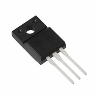
TO-220FP
TO-220
3
1
D²PAK
Application
■
3
3
1
Figure 1.
Internal schematic diagram
Switching applications
Description
The SuperFREDMesh™ series associates all
advantages of reduced on-resistance, zener gate
protection and very high dv/dt capability with a
Fast body-drain recovery diode. Such series
complements the “FDmesh™” advanced
technology.
Table 1.
Device summary
Order codes
Marking
Package
Packaging
STB9NK60ZD
B9NK60ZD
D²PAK
Tape and reel
STF9NK60ZD
F9NK60ZD
TO-220FP
Tube
STP9NK60ZD
P9NK60ZD
TO-220
Tube
April 2008
Rev 8
1/16
www.st.com
16
�Contents
STB9NK60ZD - STF9NK60ZD - STP9NK60ZD
Contents
1
Electrical ratings . . . . . . . . . . . . . . . . . . . . . . . . . . . . . . . . . . . . . . . . . . . . 3
2
Electrical characteristics . . . . . . . . . . . . . . . . . . . . . . . . . . . . . . . . . . . . . 4
2.1
Electrical characteristics (curves)
............................ 6
3
Test circuits
4
Package mechanical data . . . . . . . . . . . . . . . . . . . . . . . . . . . . . . . . . . . . 10
5
Packaging mechanical data . . . . . . . . . . . . . . . . . . . . . . . . . . . . . . . . . . 14
6
Revision history . . . . . . . . . . . . . . . . . . . . . . . . . . . . . . . . . . . . . . . . . . . 15
2/16
.............................................. 9
�STB9NK60ZD - STF9NK60ZD - STP9NK60ZD
1
Electrical ratings
Electrical ratings
Table 2.
Absolute maximum ratings
Value
Symbol
Parameter
Unit
D²PAK/TO-220
TO-220FP
VDS
Drain-source voltage (VGS = 0)
600
V
VGS
Gate- source voltage
± 30
V
Drain current (continuos) at TC = 25 °C
ID
Drain current (continuos) at TC = 100 °C
ID
IDM
(2)
PTOT
4.3
4.3
A
28
(1)
A
28
Total dissipation at TC = 25 °C
125
30
W
1
0.24
W/°C
VESD(G-S) Gate source ESD (HBM-C=100 pF, R=1.5 kΩ)
dv/dt
A
(1)
Drain current (pulsed)
Derating factor
(3)
7 (1)
7
Peak diode recovery voltage slope
VISO
Insulation withstand voltage (RMS) from all
three leads to external heat sink
(t=1 s;TC=25 °C)
Tj
Tstg
Operating junction temperature
Storage temperature
4000
V
15
V/ns
--
2500
-55 to 150
V
°C
1. Limited only by maximum temperature allowed
2. Pulse width limited by safe operating area
3.
ISD ≤ 7 A, di/dt ≤ 500 A/µs, VDD = 80%V(BR)DSS
Table 3.
Thermal data
Value
Symbol
Parameter
Unit
D²PAK/TO-220
TO-220FP
Thermal resistance junction-pcb Max
(when mounted on minimum footprint)
30
--
°C/W
Rthj-case Thermal resistance junction-case Max
1
4.16
°C/W
Rthj-pcb
Rthj-amb Thermal resistance junction-ambient Max
Tl
Table 4.
Symbol
Maximum lead temperature for soldering
purpose
62.5
°C/W
300
°C
Max value
Unit
7
A
235
mJ
Avalanche characteristics
Parameter
IAR
Avalanche current, repetitive or not-repetitive
(pulse width limited by Tj max)
EAS
Single pulse avalanche energy
(starting Tj = 25 °C, ID = IAR, VDD = 50 V)
3/16
�Electrical characteristics
2
STB9NK60ZD - STF9NK60ZD - STP9NK60ZD
Electrical characteristics
(Tcase = 25 °C unless otherwise specified)
Table 5.
Symbol
V(BR)DSS
On /off states
Parameter
Drain-source
breakdown voltage
Test conditions
ID = 1 mA, VGS = 0
Min.
Typ.
Max.
Unit
600
V
IDSS
VDS = Max rating
Zero gate voltage
drain current (VGS = 0) VDS = Max rating, TC = 125 °C
1
50
µA
µA
IGSS
Gate-body leakage
current (VDS = 0)
±10
µA
3.5
4.5
V
0.85
0.95
Ω
Typ.
Max.
Unit
VGS = ± 20 V
VGS(th)
Gate threshold voltage VDS = VGS, ID = 100 µA
RDS(on)
Static drain-source on
resistance
Table 6.
Symbol
VGS = 10 V, ID = 3.5 A
Dynamic
Parameter
Test conditions
gfs (1)
Forward
transconductance
Ciss
Coss
Crss
Input capacitance
Output capacitance
Reverse transfer
capacitance
VDS = 25 V, f = 1 MHz, VGS = 0
Equivalent output
capacitance
Total gate charge
Gate-source charge
Gate-drain charge
COSS eq(2)
Qg
Qgs
Qgd
2.5
VDS = 15 V, ID = 3.5 A
Min.
5.3
S
1110
135
30
pF
pF
pF
VGS = 0, VDS = 0 to 480 V
72
pF
VDD = 480 V, ID = 7 A,
VGS = 10 V
(see Figure 17)
41
8.7
21
53
nC
nC
nC
1. Pulsed: Pulse duration = 300 µs, duty cycle 1.5%
2. Coss eq. is defined as a constant equivalent capacitance giving the same charging time as Coss when VDS
increases from 0 to 80% VDSS
4/16
�STB9NK60ZD - STF9NK60ZD - STP9NK60ZD
Table 7.
Switching times
Symbol
Parameter
Electrical characteristics
Test conditions
Min.
Typ.
Max Unit
td(on)
tr
td(off)
tf
Turn-on delay time
Rise time
Turn-off-delay time
Fall time
VDD = 300 V, ID = 3.5 A
RG = 4.7 Ω, VGS = 10 V
(see Figure 16)
11.4
13.6
23.1
15
ns
ns
ns
ns
tr(Voff)
tf
tc
Off-voltage rise time
Fall time
Cross-over time
VDD = 480 V, ID = 7 A,
RG = 4.7 Ω, VGS = 10 V
(see Figure 16)
11
8
20
ns
ns
ns
Table 8.
Source drain diode
Symbol
Parameter
ISD
ISDM (1)
Source-drain current
Source-drain current (pulsed)
VSD (2)
Forward on voltage
ISD = 7 A, VGS = 0
Reverse recovery time
Reverse recovery charge
Reverse recovery current
ISD = 7 A, di/dt = 100 A/µs
VDD = 30 V
(see Figure 21)
130
550
8.4
ns
nC
A
Reverse recovery time
Reverse recovery charge
Reverse recovery current
ISD = 7 A, di/dt = 100 A/µs
VDD = 30 V, Tj = 150 °C
(see Figure 21)
176
880
10
ns
nC
A
trr
Qrr
IRRM
trr
Qrr
IRRM
Test conditions
Min.
Typ.
Max. Unit
7
28
A
A
1.6
V
1. Pulse width limited by safe operating area
2. Pulsed: Pulse duration = 300 µs, duty cycle 1.5%
Table 9.
Symbol
BVGSO(1)
Gate-source Zener diode
Parameter
Gate-source breakdown
voltage
Test conditions
Igs=± 1 mA (open drain)
Min
Typ
Max Unit
30
V
1. The built-in back-to-back Zener diodes have specifically been designed to enhance not only the device’s
ESD capability, but also to make them safely absorb possible voltage transients that may occasionally be
applied from gate to source. In this respect the Zener voltage is appropriate to achieve an efficient and
cost-effective intervention to protect the device’s integrity. These integrated Zener diodes thus avoid the
usage of external components
5/16
�Electrical characteristics
STB9NK60ZD - STF9NK60ZD - STP9NK60ZD
2.1
Electrical characteristics (curves)
Figure 2.
Safe operating area for TO-220 /
D²PAK
Figure 3.
Thermal impedance for TO-220 /
D²PAK
Figure 4.
Safe operating area for TO-220FP
Figure 5.
Thermal impedance for TO-220FP
Figure 6.
Output characteristics
Figure 7.
Transfer characteristics
6/16
�STB9NK60ZD - STF9NK60ZD - STP9NK60ZD
Figure 8.
Normalized BVDSS vs temperature
Electrical characteristics
Figure 9.
Static drain-source on resistance
Figure 10. Gate charge vs gate-source voltage Figure 11. Capacitance variations
Figure 12. Normalized gate threshold voltage
vs temperature
Figure 13. Normalized on resistance vs
temperature
7/16
�Electrical characteristics
Figure 14. Source-drain diode forward
characteristics
8/16
STB9NK60ZD - STF9NK60ZD - STP9NK60ZD
Figure 15. Maximum avalanche energy vs
temperature
�STB9NK60ZD - STF9NK60ZD - STP9NK60ZD
3
Test circuits
Test circuits
Figure 16. Switching times test circuit for
resistive load
Figure 17. Gate charge test circuit
Figure 18. Test circuit for inductive load
Figure 19. Unclamped inductive load test
switching and diode recovery times
circuit
Figure 20. Unclamped inductive waveform
Figure 21. Switching time waveform
9/16
�Package mechanical data
4
STB9NK60ZD - STF9NK60ZD - STP9NK60ZD
Package mechanical data
In order to meet environmental requirements, ST offers these devices in ECOPACK®
packages. These packages have a Lead-free second level interconnect. The category of
second level interconnect is marked on the package and on the inner box label, in
compliance with JEDEC Standard JESD97. The maximum ratings related to soldering
conditions are also marked on the inner box label. ECOPACK is an ST trademark.
ECOPACK specifications are available at: www.st.com
10/16
�STB9NK60ZD - STF9NK60ZD - STP9NK60ZD
Package mechanical data
TO-220 mechanical data
mm
inch
Dim
Min
A
b
b1
c
D
D1
E
e
e1
F
H1
J1
L
L1
L20
L30
∅P
Q
Typ
4.40
0.61
1.14
0.48
15.25
Max
Min
4.60
0.88
1.70
0.70
15.75
0.173
0.024
0.044
0.019
0.6
10.40
2.70
5.15
1.32
6.60
2.72
14
3.93
0.393
0.094
0.194
0.048
0.244
0.094
0.511
0.137
1.27
10
2.40
4.95
1.23
6.20
2.40
13
3.50
Max
0.181
0.034
0.066
0.027
0.62
0.050
16.40
28.90
3.75
2.65
Typ
0.409
0.106
0.202
0.051
0.256
0.107
0.551
0.154
0.645
1.137
3.85
2.95
0.147
0.104
0.151
0.116
11/16
�Package mechanical data
STB9NK60ZD - STF9NK60ZD - STP9NK60ZD
TO-220FP mechanical data
mm.
Dim.
Min.
A
4.40
inch
Typ
Max.
Min.
4.60
0.173
Typ.
0.181
Max.
B
2.5
2.7
0.098
0.106
D
2.5
2.75
0.098
0.108
E
0.45
0.70
0.017
0.027
F
0.75
1.00
0.030
0.039
F1
1.15
1.50
0.045
0.067
F2
1.15
1.50
0.045
0.067
G
4.95
5.20
0.195
0.204
G1
2.40
2.70
0.094
0.106
H
10
10.40
0.393
L2
16
0.409
0.630
28.6
30.6
1.126
L4
9.80
10.60
0.385
1.204
0.417
L5
2.9
3.6
0.114
0.141
L6
15.90
16.40
0.626
0.645
L7
9
9.30
0.354
0.366
Dia
3
3.2
0.118
0.126
B
D
A
E
L3
L3
L6
F2
H
G
G1
Dia
F
F1
L7
L2
L5
1 2 3
L4
7012510-I
12/16
�STB9NK60ZD - STF9NK60ZD - STP9NK60ZD
Package mechanical data
D²PAK (TO-263) mechanical data
mm
inch
Dim
Min
A
A1
b
b2
c
c2
D
D1
E
E1
e
e1
H
J1
L
L1
L2
R
V2
Typ
4.40
0.03
0.70
1.14
0.45
1.23
8.95
7.50
10
8.50
Max
Min
4.60
0.23
0.93
1.70
0.60
1.36
9.35
0.173
0.001
0.027
0.045
0.017
0.048
0.352
0.295
0.394
0.334
10.40
2.54
4.88
15
2.49
2.29
1.27
1.30
Max
0.181
0.009
0.037
0.067
0.024
0.053
0.368
0.409
0.1
5.28
15.85
2.69
2.79
1.40
1.75
0.192
0.590
0.099
0.090
0.05
0.051
8°
0°
0.4
0°
Typ
0.208
0.624
0.106
0.110
0.055
0.069
0.016
8°
0079457_M
13/16
�Packaging mechanical data
5
STB9NK60ZD - STF9NK60ZD - STP9NK60ZD
Packaging mechanical data
D2PAK FOOTPRINT
TAPE AND REEL SHIPMENT
REEL MECHANICAL DATA
DIM.
mm
MIN.
A
B
1.5
C
12.8
D
20.2
G
24.4
N
100
T
TAPE MECHANICAL DATA
DIM.
mm
MIN.
MAX.
MIN.
A0
10.5
10.7
0.413 0.421
B0
15.7
15.9
0.618 0.626
D
1.5
1.6
0.059 0.063
D1
1.59
1.61
0.062 0.063
E
1.65
1.85
0.065 0.073
F
11.4
11.6
0.449 0.456
K0
4.8
5.0
0.189 0.197
P0
3.9
4.1
0.153 0.161
P1
11.9
12.1
0.468 0.476
P2
1.9
2.1
0.075 0.082
MAX.
R
50
1.574
T
0.25
0.35 0.0098 0.0137
W
23.7
24.3
* on sales type
14/16
inch
0.933 0.956
inch
MAX.
MIN.
MAX.
330
12.992
13.2
0.504 0.520
26.4
0.960 1.039
0.059
0795
3.937
30.4
1.197
BASE QTY
BULK QTY
1000
1000
�STB9NK60ZD - STF9NK60ZD - STP9NK60ZD
6
Revision history
Revision history
Table 10.
Document revision history
Date
Revision
Changes
29-Sep-2003
6
Data updated
13-Jun-2006
7
The document has been reformatted
14-Apr-2008
9
– Table 8 has been corrected
– Package mechanical data upadted.
15/16
�STB9NK60ZD - STF9NK60ZD - STP9NK60ZD
Please Read Carefully:
Information in this document is provided solely in connection with ST products. STMicroelectronics NV and its subsidiaries (“ST”) reserve the
right to make changes, corrections, modifications or improvements, to this document, and the products and services described herein at any
time, without notice.
All ST products are sold pursuant to ST’s terms and conditions of sale.
Purchasers are solely responsible for the choice, selection and use of the ST products and services described herein, and ST assumes no
liability whatsoever relating to the choice, selection or use of the ST products and services described herein.
No license, express or implied, by estoppel or otherwise, to any intellectual property rights is granted under this document. If any part of this
document refers to any third party products or services it shall not be deemed a license grant by ST for the use of such third party products
or services, or any intellectual property contained therein or considered as a warranty covering the use in any manner whatsoever of such
third party products or services or any intellectual property contained therein.
UNLESS OTHERWISE SET FORTH IN ST’S TERMS AND CONDITIONS OF SALE ST DISCLAIMS ANY EXPRESS OR IMPLIED
WARRANTY WITH RESPECT TO THE USE AND/OR SALE OF ST PRODUCTS INCLUDING WITHOUT LIMITATION IMPLIED
WARRANTIES OF MERCHANTABILITY, FITNESS FOR A PARTICULAR PURPOSE (AND THEIR EQUIVALENTS UNDER THE LAWS
OF ANY JURISDICTION), OR INFRINGEMENT OF ANY PATENT, COPYRIGHT OR OTHER INTELLECTUAL PROPERTY RIGHT.
UNLESS EXPRESSLY APPROVED IN WRITING BY AN AUTHORIZED ST REPRESENTATIVE, ST PRODUCTS ARE NOT
RECOMMENDED, AUTHORIZED OR WARRANTED FOR USE IN MILITARY, AIR CRAFT, SPACE, LIFE SAVING, OR LIFE SUSTAINING
APPLICATIONS, NOR IN PRODUCTS OR SYSTEMS WHERE FAILURE OR MALFUNCTION MAY RESULT IN PERSONAL INJURY,
DEATH, OR SEVERE PROPERTY OR ENVIRONMENTAL DAMAGE. ST PRODUCTS WHICH ARE NOT SPECIFIED AS "AUTOMOTIVE
GRADE" MAY ONLY BE USED IN AUTOMOTIVE APPLICATIONS AT USER’S OWN RISK.
Resale of ST products with provisions different from the statements and/or technical features set forth in this document shall immediately void
any warranty granted by ST for the ST product or service described herein and shall not create or extend in any manner whatsoever, any
liability of ST.
ST and the ST logo are trademarks or registered trademarks of ST in various countries.
Information in this document supersedes and replaces all information previously supplied.
The ST logo is a registered trademark of STMicroelectronics. All other names are the property of their respective owners.
© 2008 STMicroelectronics - All rights reserved
STMicroelectronics group of companies
Australia - Belgium - Brazil - Canada - China - Czech Republic - Finland - France - Germany - Hong Kong - India - Israel - Italy - Japan Malaysia - Malta - Morocco - Singapore - Spain - Sweden - Switzerland - United Kingdom - United States of America
www.st.com
16/16
�