STFI20NK50Z
N-channel 500 V, 0.23 Ω, 17 A Zener-protected SuperMESH™
Power MOSFET in I²PAKFP package
Datasheet — production data
Features
Type
VDSS
RDS(on)
max
ID
PTOT
STFI20NK50Z
500 V
< 0.27 Ω
17 A
40 W
■
Fully insulated and low profile package with
increased creepage path from pin to heatsink
plate
■
Extremely high dv/dt capability
■
100% avalanche tested
■
Gate charge minimized
2
3
I2PAKFP
(TO-281)
Applications
■
1
Figure 1.
Internal schematic diagram
Switching applications
D(2)
Description
This device is an N-channel Zener-protected
Power MOSFET developed using
STMicroelectronics' SuperMESH™ technology,
achieved through optimization of ST's wellestablished strip-based PowerMESH™ layout. In
addition to a significant reduction in onresistance, this device is designed to ensure a
high level of dv/dt capability for the most
demanding applications.
G(1)
S(3)
AM01476v1
Table 1.
Device summary
Order codes
Marking
Package
Packaging
STFI20NK50Z
20NK50Z
I2PAKFP
(TO-281)
Tube
March 2012
This is information on a product in full production.
Doc ID 019007 Rev 3
1/13
www.st.com
13
�Contents
STFI20NK50Z
Contents
1
Electrical ratings . . . . . . . . . . . . . . . . . . . . . . . . . . . . . . . . . . . . . . . . . . . . 3
2
Electrical characteristics . . . . . . . . . . . . . . . . . . . . . . . . . . . . . . . . . . . . . 4
2.1
Electrical characteristics (curves)
............................. 6
3
Test circuits
4
Package mechanical data . . . . . . . . . . . . . . . . . . . . . . . . . . . . . . . . . . . . 10
5
Revision history . . . . . . . . . . . . . . . . . . . . . . . . . . . . . . . . . . . . . . . . . . . 12
2/13
............................................... 9
Doc ID 019007 Rev 3
�STFI20NK50Z
1
Electrical ratings
Electrical ratings
Table 2.
Absolute maximum ratings
Symbol
Parameter
Value
Unit
VDS
Drain-source voltage
500
V
VGS
Gate-source voltage
± 30
V
(1)
A
ID
ID
IDM
(2)
Drain current (continuous) at TC = 25 °C
Drain current (continuous) at TC = 100 °C
17
10.71
(1)
A
Drain current (pulsed)
68
A
PTOT
Total dissipation at TC = 25 °C
40
W
ESD
Gate-source human body model
(R=1,5 kΩ, C=100 pF)
6
kV
VISO
Insulation withstand voltage (RMS) from all three
leads to external heat sink (t = 1 s; TC = 25 °C)
2500
V
4.5
V/ns
-55 to 150
°C
150
°C
Value
Unit
dv/dt (3)
Tstg
Tj
Peak diode recovery voltage slope
Storage temperature
Max operating junction temperature
1. Limited by maximum junction temperature.
2. Pulse width limited by safe operating area.
3. ISD < 17 A, di/dt < 200 A/µs, VDD =80% V(BR)DSS
Table 3.
Symbol
Parameter
Rthj-case
Thermal resistance junction-case max
3.1
°C/W
Rthj-amb
Thermal resistance junction-ambient max
62.5
°C/W
Table 4.
Symbol
IAR (1)
EAS
1.
Thermal data
Avalanche characteristics
Parameter
Value
Unit
Repetitive or non repetitive avalanche current
17
A
Single pulse avalanche energy
(starting TJ=25 °C, ID=IAR, VDD=50 V)
850
mJ
Limited by maximum junction temperature.
Doc ID 019007 Rev 3
3/13
�Electrical characteristics
2
STFI20NK50Z
Electrical characteristics
(TCASE = 25 °C unless otherwise specified)
Table 5.
Symbol
On/off states
Parameter
Test conditions
Drain-source
V(BR)DSS breakdown voltage
(VGS = 0)
ID =1 mA
IDSS
Zero gate voltage
drain current (VGS = 0)
VDS = 500 V
VDS = 500 V, TC = 125 °C
IGSS
Gate-body leakage
current (VDS = 0)
VGS = ± 20 V
VGS(th)
Gate threshold voltage
VDS = VGS, ID = 100 µA
RDS(on)
Static drain-source on
resistance
VGS = 10 V, ID = 8.5 A
Table 6.
Symbol
Min.
Typ.
Max.
Unit
500
V
1
50
µA
µA
± 10
µA
3.75
4.5
V
0.23
0.27
Ω
Min.
Typ.
Max.
Unit
3
Dynamic
Parameter
Test conditions
gfs (1)
Forward transconductance
VDS = 15 V, ID = 8.5 A
-
13
S
Ciss
Coss
Crss
Input capacitance
VDS = 25 V, f = 1 MHz,
Output capacitance
V =0
Reverse transfer capacitance GS
-
2600
328
72
pF
pF
pF
Coss eq. (2)
Equivalent output
capacitance
VDS =0, VDS = 0 to 640 V
-
187
pF
td(on)
tr
td(off)
tf
Turn-on delay time
Rise time
Turn-off delay time
Fall time
VDD = 250 V, ID = 8.5 A,
RG = 4.7 Ω, VGS = 10 V
(see Figure 15)
-
28
20
70
15
ns
ns
ns
ns
Qg
Qgs
Qgd
Total gate charge
Gate-source charge
Gate-drain charge
VDD = 400 V, ID = 17 A,
VGS = 10 V
(see Figure 16)
-
85
15.5
42
119
nC
nC
nC
1. Pulsed: pulse duration=300µs, duty cycle 1.5%
2. Coss eq. is defined as a constant equivalent capacitance giving the same charging time as Coss when VDS
increases from 0 to 80% VDSS.
4/13
Doc ID 019007 Rev 3
�STFI20NK50Z
Electrical characteristics
Table 7.
Symbol
Source drain diode
Parameter
Test conditions
Min.
Typ.
Max.
Unit
-
17
68
A
A
1.6
V
ISD
ISDM(1)
Source-drain current
Source-drain current (pulsed)
VSD(2)
Forward on voltage
ISD = 17 A, VGS = 0
-
Reverse recovery time
Reverse recovery charge
Reverse recovery current
ISD = 17 A,
di/dt = 100 A/µs
VR = 100 V
(see Figure 17)
-
355
3.90
22
ns
µC
A
Reverse recovery time
Reverse recovery charge
Reverse recovery current
ISD = 17 A,
di/dt = 100 A/µs
VR = 100 V, Tj = 150 °C
(see Figure 17)
-
440
5.72
26
ns
µC
A
trr
Qrr
IRRM
trr
Qrr
IRRM
1. Pulsed: pulse duration=300µs, duty cycle 1.5%
2. Pulse width limited by safe operating area.
Table 8.
Symbol
V(BR)GSO
Gate-source Zener diode
Parameter
Test conditions
Gate-source breakdown voltage
IGS= ± 1mA
(ID = 0)
Min.
30
Typ.
Max.
-
Unit
V
The built-in back-to-back Zener diodes have specifically been designed to enhance not only
the device’s ESD capability, but also to make them safely absorb possible voltage transients
that may occasionally be applied from gate to source. In this respect the Zener voltage is
appropriate to achieve an efficient and cost-effective intervention to protect the device’s
integrity. These integrated Zener diodes thus avoid the usage of external components.
Doc ID 019007 Rev 3
5/13
�Electrical characteristics
STFI20NK50Z
2.1
Electrical characteristics (curves)
Figure 2.
Safe operating area
Figure 3.
Thermal impedance
Figure 4.
Output characteristics
Figure 5.
Transfer characteristics
Figure 6.
Transconductance
Figure 7.
Static drain-source on resistance
6/13
Doc ID 019007 Rev 3
�STFI20NK50Z
Figure 8.
Electrical characteristics
Gate charge vs gate-source voltage Figure 9.
Figure 10. Normalized gate threshold voltage
vs temperature
-;�����
H9E�fZ�
H6E/H9E
;6 /#""g3
�`ad_�
Capacitance variations
Figure 11. Normalized on resistance vs
temperature
�`ad_�
���
���
�
���
���
���
���
���
���
���
���
ª��� ª��
�
��
���
��� F
很抱歉,暂时无法提供与“STFI20NK50Z”相匹配的价格&库存,您可以联系我们找货
免费人工找货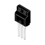


 工商网监
湘ICP备2023018690号
工商网监
湘ICP备2023018690号