STG3159
Low voltage 1Ω max single SPDT switch
with break-before-make feature
Features
■
High speed:
– tPD = 1.5ns (Typ.) at VCC = 3.0V
– tPD = 1.5ns (Typ.) at VCC = 2.3V
■
Ultra low power dissipation:
– ICC = 0.2µA (Max.) at TA = 85°C
■
Low "ON" resistance:
– RON = 1.0Ω (TA = 25ºC) at VCC = 4.3V
– RON = 1.1Ω (TA = 25ºC) at VCC = 3.0V
– RON = 1.7Ω (TA = 25ºC) at VCC = 1.8V
■
Wide operating voltage range:
– VCC (OPR) = 1.65V to 4.5V single supply
■
4.5V Tolerant and 1.8V compatible threshold
on digital control input at VCC = 2.3V to 3.0V
■
Latch-up performance exceeds 100mA per
JESD 78, Class II
■
ESD Performance tested per JESD22
– 2000V Human-body model
(A114-B, Class II)
– 200V Machine model (A115-A)
– 1000V Charged-device model (C101)
)
s
(
ct
u
d
o
r
P
e
t
e
l
o
s
b
O
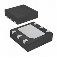
DFN6L
Description
c
u
d
)
s
t(
The STG3159 is a high-speed CMOS low voltage
single analog S.P.D.T. (Single Pole Dual Throw)
switch or 2:1 Multiplexer /Demultiplexer switch
fabricated in silicon gate C2MOS technology. It is
designed to operate from 1.65V to 4.3V, making
this device ideal for portable applications.
e
t
le
o
r
P
o
s
b
O
-
The device offers very low ON-Resistance (1Ω) at
VCC = 4.3V. The SEL inputs are provided to
control the switch. The switch S1 is ON (they are
connected to common Ports Dn) when the SEL
input is held high and OFF (high impedance state
exists between the two ports) when SEL is held
low; the switch S2 is ON (it is connected to
common Port D) when the SEL input is held low
and OFF (high impedance state exists between
the two ports) when SEL is held high.
Additional key features are fast switching speed,
break-before-make delay time and Ultra Low
Power Consumption. All inputs and outputs are
equipped with protection circuits against static
discharge, giving them ESD immunity and
transient excess voltage.
Order codes
Part number
Package
Packaging
STG3159DTR
DFN6L (1.2mm x 1mm)
Tape and Reel
December 2006
Rev 1
1/18
www.st.com
18
�Contents
STG3159
Contents
1
Pin connections and functions . . . . . . . . . . . . . . . . . . . . . . . . . . . . . . . . 3
2
Electrical ratings . . . . . . . . . . . . . . . . . . . . . . . . . . . . . . . . . . . . . . . . . . . . 4
3
Electrical characteristics . . . . . . . . . . . . . . . . . . . . . . . . . . . . . . . . . . . . . 5
3.1
DC electrical characteristics . . . . . . . . . . . . . . . . . . . . . . . . . . . . . . . . . . . . 5
3.2
AC electrical characteristics . . . . . . . . . . . . . . . . . . . . . . . . . . . . . . . . . . . . 7
3.3
Analog switch characteristics . . . . . . . . . . . . . . . . . . . . . . . . . . . . . . . . . . . 8
4
Test circuits
............................................... 9
5
Package mechanical data . . . . . . . . . . . . . . . . . . . . . . . . . . . . . . . . . . . . 12
6
Revision history . . . . . . . . . . . . . . . . . . . . . . . . . . . . . . . . . . . . . . . . . . . 17
c
u
d
e
t
le
)
s
(
ct
u
d
o
r
P
e
t
e
l
o
s
b
O
2/18
o
s
b
O
-
o
r
P
)
s
t(
�STG3159
1
Pin connections and functions
Pin connections and functions
Figure 1.
Pin connections (top through view)
SEL
SEL
11
66
VCC
VCC
22
55 GND
GND
D
D
3
4
S1
S1
S2
S2
DFN6L
Table 1.
Truth table
c
u
d
Sel
Switch S1
Switch S2
H
ON
OFF (1)
L
OFF (1)
1. High impedance
Table 2.
Pin descriptions
Symbol
6, 4
S1, S2
3
D
(s)
1
ct
2
5
o
r
P
e
du
e
t
le
o
s
b
O
-
Pin Nº
Figure 2.
)
s
t(
o
r
P
ON
Name and function
Independent channels
Common channels
SEL
Control
VCC
Positive supply voltage
GND
Ground (0V)
Input equivalent circuit
t
e
l
o
s
b
O
3/18
�Electrical ratings
2
STG3159
Electrical ratings
Stressing the device above the rating listed in the “Absolute Maximum Ratings” table may
cause permanent damage to the device. These are stress ratings only and operation of the
device at these or any other conditions above those indicated in the Operating sections of
this specification is not implied. Exposure to Absolute Maximum Rating conditions for
extended periods may affect device reliability. Refer also to the STMicroelectronics SURE
Program and other relevant quality documents.
Table 3.
Absolute maximum ratings
Symbol
VCC
Parameter
-0.5 to 5.5
V
-0.5 to VCC + 0.5
V
-0.5 to 5.5
V
Supply voltage
DC Input voltage
VIC
DC Control input voltage
VO
DC Output voltage
IIKC
DC Input diode current on control pin (VSEL < 0V)
-50
IIK
DC Input diode current (VSEL < 0V)
±50
IOK
DC Output diode current
IO
DC Output current
IOP
DC Output current peak
(pulse at 1ms, 10% duty cycle)
-0.5 to VCC + 0.5
so
Tstg
Storage temperature
(s)
Lead temperature (10 sec)
)
s
t(
V
mA
mA
±20
mA
±200
mA
±400
mA
±100
mA
1120
mW
-65 to 150
°C
300
°C
Value
Unit
1.65 to 4.5
V
P
e
let
b
O
-
Power dissipation at TA = 70ºC (1)
c
u
d
ro
DC VCC or ground current
PD
TL
t
c
u
Derate above 70ºC by 18.5mW/C
1.
d
o
r
P
e
Table 4.
Recommended operating conditions
Symbol
t
e
l
o
VCC
Supply voltage
Parameter
(1)
VI
Input voltage
0 to VCC
V
VIC
Control input voltage
0 to 4.5
V
VO
Output voltage
0 to VCC
V
Top
Operating temperature
-55 to 125
°C
dt/dv
Input rise and fall time
control input
1. Truth table guaranteed: 1.2V to 4.5V
4/18
Unit
VI
ICC or IGND
s
b
O
Value
VCC = 1.65V to
2.7V
0 to 20
VCC = 3.0 to 4.5V
0 to 10
ns/V
�STG3159
Electrical characteristics
3
Electrical characteristics
3.1
DC electrical characteristics
Table 5.
DC specifications
Test conditions
Symbol
Value
Parameter
TA = 25°C
-40 to 85°C
-55 to 125°C
Min.
Min.
Unit
Vcc (V)
Min.
VIH
High level
input
voltage
VIL
Low level
input
voltage
RPEAK
RON
0.65VCC
0.65VCC
2.3-2.5
1.2
1.2
1.2
2.7-3.0
1.3
1.3
1.3
3.3-3.6
1.4
1.4
1.4
4.3
1.6
1.6
1.6
1.65-1.95
0.40
0.40
2.3-2.5
0.60
0.60
2.7-3.0
0.60
0.60
3.3-3.6
0.60
4.3
0.80
2.7
3.0
2.2
VS = 0V to
VCC
IS = 100mA
O
bs
t
e
l
o
∆RON
(s)
RFLAT
1.6
0.80
1.8
1.5
1.7
1.1
1.2
1.4
1.7
2.3
2.7
1.5
1.7
2.7
VS = 1.3V
IS = 100mA
1.2
3.0
t
c
u
VS = 1.5V
IS = 100mA
1.1
1.2
1.6
4.3
VS = 2.5V
IS = 100mA
1.0
1.1
1.3
od
3.0
VS @ RON
Max
IS = 100mA
4.3
2.7
3.0
4.3
V
)
s
t(
0.40
od
uc
0.60
0.60
V
0.60
0.80
Ω
Ω
0.06
1.8
2.7
Max.
3.5
VS = 0.9V
IS = 100mA
0.05
Ω
0.05
0.05
1.8
ON
resistance
flatness (2)
so
b
O
1.2
e
t
le
3.0
1.3
Pr
0.60
1.8
r
P
e
ON
resistance
match
between
channels (1)
Max.
0.65VCC
4.3
Switch On
resistance
Max.
1.65-1.95
1.8
Switch ON
peak
resistance
Typ.
VS = 0V to
VCC
IS = 100mA
1.0
1.5
1.5
0.45
0.60
0.70
0.40
0.50
0.60
0.37
0.50
0.60
Ω
5/18
�Electrical characteristics
Table 5.
STG3159
DC specifications (continued)
Test conditions
Symbol
Value
Parameter
TA = 25°C
-40 to 85°C
-55 to 125°C
Min.
Min.
Unit
Vcc (V)
Min.
IOFF
OFF state
leakage
current
(SN), (D)
IIN
Input
leakage
current
ICC
Quiescent
supply
current
ICCLV
Quiescent
supply
current low
voltage
driving
Typ.
Max.
Max.
Max.
4.3
VS = 0.3 or
4V
±20
±100
nA
0 – 4.3
VSEL = 0 to
4.3V
±0.1
±1
µA
1.65 – 4.3
VSEL =
VCC or
GND
±0.05
±0.2
4.3
VSEL =
1.65V
±17
±35
±70
4.3
VSEL =
1.80V
±15
±30
±60
4.3
VSEL =
2.60V
±5
±10
±20
uc
2. Flatness is defined as the difference between the maximum and minimum value of ON-resistance as measured over the
specified analog signal ranges.
)
s
(
ct
u
d
o
r
P
e
t
e
l
o
s
b
O
6/18
o
s
b
O
-
µA
)
s
t(
d
o
r
P
e
let
1. ∆RON = RON(Max) - RON(Min)
±1
µA
�STG3159
Electrical characteristics
3.2
AC electrical characteristics
Table 6.
AC Electrical characteristics (CL = 35pF, RL = 50Ω, tr = tf ≤5ns)
Test conditions
Symbol
Value
Parameter
TA = 25°C
-40 to 85°C
-55 to 125°C
Unit
Vcc (V)
Min.
1.65-1.95
tPLH,
tPHL
Propagation
delay
Min.
Max.
Min.
Max.
0.14
VS = OPEN
3.6-4.3
ns
0.13
0.13
VS = 0.8V
1.65-1.95
36
2.3-2.7
tON
Max.
0.15
2.3-2.7
3.0-3.3
Typ.
22
32
42
16
26
36
13
23
33
VS = 1.5V
3.0-3.3
3.6-4.3
VS = 0.8
1.65-1.95
2.3-2.7
VS = 1.5V
3.0-3.3
3.6-4.3
1.65-1.95
17
27
12
23
11
21
Break before
make time delay
tD
15
CL = 35pF
RL = 50Ω
VS = 1.5V
2.3-2.7
3.0-3.3
3.6-4.3
1.65
Charge injection
3
d
o
r
P
e
4.3
e
t
le
o
s
b
O
-
CL = 100pF
VGEN = 0V
RGEN = 0Ω
uc
2.3
Q
(t s)
c
u
d
29
Turn-OFF time
tOFF
)
s
t(
ns
Turn-ON time
10
o
r
P
37
ns
33
31
ns
8
6
16
22
pC
26
33
t
e
l
o
s
b
O
7/18
�Electrical characteristics
STG3159
3.3
Analog switch characteristics
Table 7.
Analog switch characteristics (CL = 5pF, RL = 50Ω, TA = 25°C)
Test conditions
Symbol
Value
Parameter
TA = 25°C
-40 to 85°C
-55 to 125°C
Min.
Min.
Unit
Vcc (V)
Min.
Typ.
Max.
Max.
Max.
1.65-4.3
VS = 1VRMS
f = 100kHz
-80
dB
1.6-4.3
VS = 1VRMS
f = 100kHz
-80
dB
THD
Total
harmonic
distortion
2.3-4.3
RL = 600Ω
VS = 2VPP
f = 20Hz to 20
kHz
0.03
%
BW
-3dB
bandwidth
1.65-4.3
RL= 50Ω
150
CIN
Control pin
input
capacitance
CON
Sn port
capacitance
when switch is
enabled
COFF
Sn port
capacitance
when switch is
disabled
3.3
D Port
Capacitance
when Switch
is Enabled
3.3
Off Isolation
OIRR
(1)
Xtalk
Crosstalk
CD
6
3.3
f = 1MHz
f = 1MHz
r
P
e
u
d
o
)
s
(
ct
f = 1MHz
s
b
O
8/18
e
t
le
52
o
s
b
O
25
50
1. OFF Isolation = 20Log10 (VD/VS), VD = output. VS = input to OFF switch.
t
e
l
o
c
u
d
)
s
t(
MHz
o
r
P
pF
�STG3159
Test circuits
4
Test circuits
Figure 3.
ON-Resistance
Figure 5.
Figure 4.
OFF Leakage
Figure 6.
Bandwidth
c
u
d
Channel to channel crosstalk
e
t
le
)
s
(
ct
Figure 7.
)
s
t(
o
r
P
o
s
b
O
-
u
d
o
r
P
e
OFF Isolation
t
e
l
o
s
b
O
9/18
�Test circuits
STG3159
Figure 8.
Note:
Test circuit
CL = 5/35pF or equivalent: (includes jig capacitance)
RL = 50Ω or equivalent
c
u
d
RT = ZOUT of pulse generator (typically 50Ω)
Figure 9.
Break-before-make time delay
e
t
le
)
s
(
ct
u
d
o
r
P
e
o
s
b
O
-
Figure 10. Switching time and charge injection
(VGEN = 0V, RGEN = 0Ω, RL = 1MΩ, CL = 100pF)
t
e
l
o
s
b
O
10/18
o
r
P
)
s
t(
�STG3159
Test circuits
Figure 11. Turn ON, turn OFF delay time
c
u
d
e
t
le
)
s
(
ct
)
s
t(
o
r
P
o
s
b
O
-
u
d
o
r
P
e
t
e
l
o
s
b
O
11/18
�Package mechanical data
5
STG3159
Package mechanical data
In order to meet environmental requirements, ST offers these devices in ECOPACK®
packages. These packages have a Lead-free second level interconnect. The category of
second level interconnect is marked on the package and on the inner box label, in
compliance with JEDEC Standard JESD97. The maximum ratings related to soldering
conditions are also marked on the inner box label. ECOPACK is an ST trademark.
ECOPACK specifications are available at: www.st.com
c
u
d
e
t
le
)
s
(
ct
u
d
o
r
P
e
t
e
l
o
s
b
O
12/18
o
s
b
O
-
o
r
P
)
s
t(
�STG3159
Package mechanical data
Table 8.
DFN6 (1.2mm x 1mm) Mechanical data
mm.
inch
Dim.
Typ.
Min.
Max.
Typ.
Min.
Max.
A
0.50
0.45
0.55
0.019
0.017
0.021
A1
0.02
0
0.05
0.001
0
0.002
A3
0.127
b
0.20
0.15
0.25
0.007
0.006
0.010
D
1.20
1.10
1.30
0.047
0.043
0.051
E
1
0.90
1.10
0.039
0.035
0.043
e
0.40
L
0.35
0.30
0.40
0.013
0.011
0.015
L1
0.45
0.40
0.50
0.017
0.015
0.019
0.005
0.015
Figure 12. Package dimensions
c
u
d
e
t
le
)
s
(
ct
)
s
t(
o
r
P
o
s
b
O
-
u
d
o
r
P
e
t
e
l
o
s
b
O
13/18
�Package mechanical data
Table 9.
STG3159
DFN6 Foot print recommendation
c
u
d
e
t
le
)
s
(
ct
u
d
o
r
P
e
t
e
l
o
s
b
O
14/18
o
s
b
O
-
o
r
P
)
s
t(
�STG3159
Package mechanical data
Table 10.
DFN6L Tape information
Dim
mm.
inch
D
1.50 +0.1/0
0.059 +0.004/0
E
1.75 ±0.1
0.069 ±0.004
Po
4.00 ±0.1
0.157 ±0.004
T max.
0.40
0.016
D1 min.
1
0.039
F
3.5 ±0.05
0.138 ±0.002
K max.
2.40
0.094
P2
2.00 ±0.05
0.079 ±0.002
R
25
0.984
W
8.00 ±0.30
0.315 ±0.012
P1
4.00
0.157
Ao, Bo, Ko
0.05 min to 0.50 max.
0.002 min to 0.020 max.
Figure 13. DFN6L Tape information
e
t
le
)
s
(
ct
c
u
d
)
s
t(
o
r
P
o
s
b
O
-
u
d
o
r
P
e
t
e
l
o
s
b
O
15/18
�Package mechanical data
Table 11.
STG3159
DFN6L Reel information
Dim
mm.
inch
Tape size
8.0 ±0.30
0.315 ±0.012
A max.
180.0
7.086
B min.
1.5
0.059
C
13.0 ±0.20
0.512 ±0.008
D min.
20.2
0.795
N min.
60
2.362
G
8.4 +2/-0
0.319 +0.079/-0
T max.
14.4
0.567
Figure 14. DFN6L Reel information
c
u
d
e
t
le
)
s
(
ct
u
d
o
r
P
e
t
e
l
o
s
b
O
16/18
o
s
b
O
-
o
r
P
)
s
t(
�STG3159
6
Revision history
Revision history
Table 12.
Revision history
Date
Revision
06-Dec-2006
1
Changes
First release
c
u
d
e
t
le
)
s
(
ct
)
s
t(
o
r
P
o
s
b
O
-
u
d
o
r
P
e
t
e
l
o
s
b
O
17/18
�STG3159
Please Read Carefully:
Information in this document is provided solely in connection with ST products. STMicroelectronics NV and its subsidiaries (“ST”) reserve the
right to make changes, corrections, modifications or improvements, to this document, and the products and services described herein at any
time, without notice.
All ST products are sold pursuant to ST’s terms and conditions of sale.
)
s
t(
Purchasers are solely responsible for the choice, selection and use of the ST products and services described herein, and ST assumes no
liability whatsoever relating to the choice, selection or use of the ST products and services described herein.
c
u
d
No license, express or implied, by estoppel or otherwise, to any intellectual property rights is granted under this document. If any part of this
document refers to any third party products or services it shall not be deemed a license grant by ST for the use of such third party products
or services, or any intellectual property contained therein or considered as a warranty covering the use in any manner whatsoever of such
third party products or services or any intellectual property contained therein.
e
t
le
o
r
P
UNLESS OTHERWISE SET FORTH IN ST’S TERMS AND CONDITIONS OF SALE ST DISCLAIMS ANY EXPRESS OR IMPLIED
WARRANTY WITH RESPECT TO THE USE AND/OR SALE OF ST PRODUCTS INCLUDING WITHOUT LIMITATION IMPLIED
WARRANTIES OF MERCHANTABILITY, FITNESS FOR A PARTICULAR PURPOSE (AND THEIR EQUIVALENTS UNDER THE LAWS
OF ANY JURISDICTION), OR INFRINGEMENT OF ANY PATENT, COPYRIGHT OR OTHER INTELLECTUAL PROPERTY RIGHT.
o
s
b
O
-
UNLESS EXPRESSLY APPROVED IN WRITING BY AN AUTHORIZED ST REPRESENTATIVE, ST PRODUCTS ARE NOT
RECOMMENDED, AUTHORIZED OR WARRANTED FOR USE IN MILITARY, AIR CRAFT, SPACE, LIFE SAVING, OR LIFE SUSTAINING
APPLICATIONS, NOR IN PRODUCTS OR SYSTEMS WHERE FAILURE OR MALFUNCTION MAY RESULT IN PERSONAL INJURY,
DEATH, OR SEVERE PROPERTY OR ENVIRONMENTAL DAMAGE. ST PRODUCTS WHICH ARE NOT SPECIFIED AS "AUTOMOTIVE
GRADE" MAY ONLY BE USED IN AUTOMOTIVE APPLICATIONS AT USER’S OWN RISK.
)
s
(
ct
u
d
o
Resale of ST products with provisions different from the statements and/or technical features set forth in this document shall immediately void
any warranty granted by ST for the ST product or service described herein and shall not create or extend in any manner whatsoever, any
liability of ST.
r
P
e
t
e
l
o
ST and the ST logo are trademarks or registered trademarks of ST in various countries.
Information in this document supersedes and replaces all information previously supplied.
bs
The ST logo is a registered trademark of STMicroelectronics. All other names are the property of their respective owners.
O
© 2006 STMicroelectronics - All rights reserved
STMicroelectronics group of companies
Australia - Belgium - Brazil - Canada - China - Czech Republic - Finland - France - Germany - Hong Kong - India - Israel - Italy - Japan Malaysia - Malta - Morocco - Singapore - Spain - Sweden - Switzerland - United Kingdom - United States of America
www.st.com
18/18
�


 工商网监
湘ICP备2023018690号
工商网监
湘ICP备2023018690号
