STG4160
Low voltage 0.5 Ω single SPDT switch with break-before-make
feature and 15 kV contact ESD protection
Datasheet - production data
Applications
• Mobile phones
Description
The STG4160 device is a high-speed CMOS low
voltage single analog SPDT (single pole dual
throw) switch or 2:1 multiplexer/demultiplexer
switch fabricated in silicon gate C2MOS
technology. It is designed to operate from 1.65 to
4.8 V, making this device ideal for portable
applications. It offers low on-resistance (0.40 Ω
typ.) at VCC = 4.3 V. The SEL inputs are provided
to control the switches.
Flip Chip 8
Features
• Wide operating voltage range:
VCC (opr.) = 1.65 to 4.8 V
• Low power dissipation:
ICC = 0.2 µA (max.) at TA = 85 °C
• Low on-resistance:
– RON = 0.75 Ω (TA = 25 °C)
at VCC = 2.25 V
– RON = 0.50 Ω (TA = 25 °C) at VCC = 3.0 V
– RON = 0.40 Ω (TA = 25 °C) at VCC = 4.3 V
• Separate supply voltage for switch and control
pins
• Latch-up performance exceeds 100 mA per
JESD 78, Class II
• ESD performance tested on common pin
(D pin):
– 15 kV IEC 61000-4-2 ESD, contact
discharge
– 8 kV HBM JESD22 A114-B Class II
• ESD performance tested on S1 and S2 pin:
8 kV IEC 61000-4-2 ESD, contact discharge
The switch S1 is ON (connected to the common
port D) when the SEL input is held high and OFF
(high impedance state exists between the two
ports) when the SEL is held low. The switch S2 is
ON (connected to the common port D) when the
SEL input is held low and OFF (high impedance
state exist between the two ports) when the SEL
is held high.
Additional key features are fast switching speed,
break-before-make delay time and ultra power
consumption. All inputs and outputs are equipped
with protection circuits against static discharge,
giving them ESD immunity and transient excess
voltage.
Table 1. Device summary
Order code
Package
Packing
STG4160BJR
Flip Chip 8
Tape and reel
• ESD performance test on all other pins:
– 4 kV HBM (JESD22 A114-B Class II)
– 400 V machine model (JESD22 A115-A)
– 1500 V charged-device model
(JESD22 C101)
July 2022
This is information on a product in full production.
DocID15013 Rev 4
1/19
www.st.com
19
�Contents
STG4160
Contents
1
Pin settings . . . . . . . . . . . . . . . . . . . . . . . . . . . . . . . . . . . . . . . . . . . . . . . . 3
1.1
Pin connections . . . . . . . . . . . . . . . . . . . . . . . . . . . . . . . . . . . . . . . . . . . . . 3
1.2
Pin description . . . . . . . . . . . . . . . . . . . . . . . . . . . . . . . . . . . . . . . . . . . . . . 3
2
Logic diagram . . . . . . . . . . . . . . . . . . . . . . . . . . . . . . . . . . . . . . . . . . . . . . 4
3
Maximum ratings . . . . . . . . . . . . . . . . . . . . . . . . . . . . . . . . . . . . . . . . . . . . 5
4
Electrical characteristics . . . . . . . . . . . . . . . . . . . . . . . . . . . . . . . . . . . . . 6
5
Test circuits . . . . . . . . . . . . . . . . . . . . . . . . . . . . . . . . . . . . . . . . . . . . . . . . 9
6
Package information . . . . . . . . . . . . . . . . . . . . . . . . . . . . . . . . . . . . . . . . 13
7
Package marking information . . . . . . . . . . . . . . . . . . . . . . . . . . . . . . . . 17
8
Revision history . . . . . . . . . . . . . . . . . . . . . . . . . . . . . . . . . . . . . . . . . . . 18
2/19
DocID15013 Rev 4
�STG4160
Pin settings
1
Pin settings
1.1
Pin connections
Figure 1. Pin connections
%XPS�YLHZ
7R S�YLHZ
9/
�
�
9&&
�
6�
�
�
6(/
*1'
�
�
'�
�
�
*1'
6��
6��
�
�
*1'
�
�
'�
6��
�
�
6(/�
9/
�
�
9 &&
*1'
&6�����
1.2
Pin description
Table 2. Pin assignment
Pin number
Ball number
Symbol
1
B1
S1
2
B2
GND
3
B3
S2
Independent channel
4
B4
VL
Logic supply voltage
5
A4
VCC
Positive supply voltage
6
A3
SEL
Control
7
A2
D
8
A1
GND
DocID15013 Rev 4
Name and function
Independent channel
Ground (0 V)
Common channel
Ground (0 V)
3/19
�Logic diagram
2
STG4160
Logic diagram
Figure 2. Functional diagram
�6�
'
�6�
6(/
$0�����
Figure 3. Circuit equivalent logic
6�
'
6�
6(/
$0�����
Table 3. Truth table
SEL
Switch S1
Switch S2
H
ON
OFF(1)
L
OFF(1)
ON
1. High impedance.
4/19
DocID15013 Rev 4
�STG4160
3
Maximum ratings
Maximum ratings
Stressing the device above the rating listed in Table 4: Absolute maximum ratings may
cause permanent damage to the device. These are stress ratings only and operation of the
device at these or any other conditions above those indicated in Table 5: Recommended
operating conditions of this specification is not implied. Exposure to absolute maximum
rating conditions for extended periods may affect device reliability. Refer also to the
STMicroelectronics® SURE program and other relevant quality documents.
Table 4. Absolute maximum ratings
Symbol
Value
Unit
Supply voltage
-0.5 to 5.5
V
VL
Logic supply voltage
-0.5 to 5.5
V
VI
DC input voltage
-0.5 to VCC + 0.5
V
VIC
DC control input voltage
-0.5 to VL + 5.5
V
VO
DC output voltage
-0.5 to VCC + 0.5
V
IIKC
DC input diode current on control pin (VSEL < 0 V)
- 50
mA
IIK
DC input diode current (VSEL < 0 V)
± 50
mA
IOK
DC output diode current
± 20
mA
IO
DC output current
± 300
mA
IOP
DC output current peak (pulse at 1 ms, 10% duty cycle)
± 500
mA
± 100
mA
500
mW
-65 to 150
°C
260
°C
Value
Unit
Supply voltage
1.65 to 4.8
V
VL
Logic supply voltage(1)
1.65 to VCC
V
VI
Input voltage
0 to VCC
V
VIC
Control input voltage
0 to VL
V
VO
Output voltage
0 to VCC
V
Top
Operating temperature
-40 to 85
°C
VCC
Parameter
ICC or IGND DC VCC or ground current
1.
PD
Power dissipation at TA = 70
Tstg
Storage temperature
TL
Lead temperature (10 sec.)
°C(1)
Derate above 70 °C by 18.5 mW/C.
Table 5. Recommended operating conditions
Symbol
VCC
dt/dv
Parameter
Input rise and fall time control input
VL = 1.65 to 2.7 V
0 to 20
VL= 3.0 to 4.8 V
0 to 10
ns/V
1. VL pin should not be left floating.
DocID15013 Rev 4
5/19
�Electrical characteristics
4
STG4160
Electrical characteristics
Table 6. DC specifications
Value
Symbol
VIH
VIL
Parameter
High level input
voltage
Low level input
voltage
VCC (V)
VL (V)
Test conditions
TA = 25 °C
Min.
Typ. Max. Min.
1.65 – 1.95
1.25
1.25
2.3 – 2.7
1.75
1.75
3.0 – 3.6
2.34
2.34
4.3
2.80
2.80
V
1.65 – 1.95
0.6
0.6
2.3 – 2.7
0.8
0.8
3.0 – 3.6
1.05
1.05
4.3
1.5
1.5
1.5
2.5
3.7
0.75
1.0
1.3
0.50
0.65
0.8
3.7
0.45
0.55
0.7
4.3
0.40
0.5
0.65
1.8
40
1.65 – 4.3
V
2.25
ΔRON
On-resistance
On-resistance
match between
channels(1)
3
1.65 – 4.3
VS = 0 V to VCC
IS = 100 mA
2.25
3
RFLAT
1.65 – 4.3
10
mΩ
3.7
10
4.3
10
1.8
1.0
1.7
2.0
300
430
550
150
190
270
3.7
140
180
230
4.3
140
180
220
3
Ω
20
VS = 0 V to VCC
IS = 100 mA
2.25
On-resistance
flatness(2)
Max.
1.65 – 4.3
1.8
RON
-40 to 85 °C Unit
1.65 – 4.3
VS = 0 V to VCC
IS = 100 mA
mΩ
IOFF
Sn OFF state
leakage current
4.3
4.3
VS = 0.3 to 4.0
VD = 0.3 to 4.0
-30
30
-300
300
nA
ION
Sn ON state
leakage current
4.3
4.3
VS = 0.3 to 4.0
VD = open
-30
30
-300
300
nA
ID
D ON state
leakage current
4.3
4.3
VS = open
VD = 0 to 4.0
-30
30
-300
300
nA
6/19
DocID15013 Rev 4
�STG4160
Electrical characteristics
Table 6. DC specifications (continued)
Value
Symbol
Parameter
VCC (V)
VL (V)
Test conditions
TA = 25 °C
-40 to 85 °C Unit
Min.
Typ. Max. Min.
Max.
ICC
Quiescent
supply current
1.65 – 4.3
1.65 – 4.3
VSEL = VCC or GND
-0.05
0.05
-0.2
0.2
μA
ISEL
SEL leakage
current
1.65 – 4.3
1.65 – 4.3
VSEL= 4.3V or GND
-0.2
0.2
-2
2
μA
1.
ΔRON = RON(Max) - RON(Min).
2.
Flatness is defined as the difference between the maximum and minimum value of on-resistance as measured over the specified analog
signal ranges.
Table 7. AC electrical characteristics (CL = 35 pF, RL = 50 Ω, tr = tf ≤ 5 ns)
Test conditions
Symbol
Value
Parameter
TA = 25 °C
VCC (V)
Min.
1.65 – 1.95
tPLH,
tPHL
Propagation
delay
2.3 – 2.7
0.12
3.6 – 4.3
0.12
1.65 – 4.3
3 – 3.6
VS = VCC
RL = 50 Ω
CL = 30 pF
2.3 – 2.7
Turn-off time
1.65 – 4.3
3 – 3.6
VS = VCC
RL = 50 Ω
CL = 30 pF
1.65 – 1.95
2.3 – 2.7
1.65 – 4.3
3 – 3.6
CL = 35 pF
RL = 50 Ω
VS = VCC/2
4.3
1.65 – 1.95
Charge
injection
123
160
48
62
80
33
43
56
29
38
49
36
45
60
35
47
62
30
40
51
29
38
50
10
42
10
22
5
15
5
12
ns
75
2.3 – 2.7
1.65 – 4.3
3.0 – 3.3
70
ns
4.3
Q
Max.
ns
1.65 – 1.95
Break-beforemake time
delay
Min.
ns
3.0 – 3.3
4.3
tD
Max.
0.14
2.3 – 2.7
tOFF
Typ.
1.65 – 4.3
Turn-on time
Unit
0.18
1.65 – 1.95
tON
-40 to 85 °C
VL (V)
CL = 1 nF
VGEN = 0 V
3.6 – 4.3
98
pC
133
162
DocID15013 Rev 4
7/19
�Electrical characteristics
STG4160
Table 7. AC electrical characteristics (CL = 35 pF, RL = 50 Ω, tr = tf ≤ 5 ns) (continued)
Test conditions
Symbol
Value
Parameter
TA = 25 °C
VCC (V)
Min.
OIRR
Xtalk
1.
OFF-isolation(1)
Crosstalk
-40 to 85 °C
Unit
VL (V)
1.65 – 4.3
1.65 – 4.3
4.3
4.3
Typ.
Max.
Min.
Max.
VS = 1 VRMS
f = 100 kHz
77
VS = 1 VRMS
f = 1 MHz
67
VS = 1 VRMS
f = 5 MHz
50
VS = 1 VRMS
f = 100 kHz
80
VS = 1 VRMS
f = 1 MHz
67
VS = 1 VRMS
f = 5 MHz
50
0.01
%
50
MHz
THD
Total harmonic
distortion
2.3 – 4.3
4.3
RL = 600 Ω
CL = 50 pF
VS = VCC
f = 600 Hz to
20 kHz
BW
-3 dB
Bandwidth
(switch ON)
1.65 – 4.3
4.3
RL = 50 Ω
dB
dB
OFF-isolation = 20 log10 (VD/VS), VD = output, VS = input to off switch.
Table 8. Capacitive characteristics
Test conditions
Symbol
Value
Parameter
TA = 25 °C
VCC (V)
-40 to 85 °C
Unit
VL (V)
Min.
Typ.
Max.
Min.
Max.
CSEL
Control pin
input
capacitance
1.8 – 4.3
1.8 – 4.3
VL = VCC
30
pF
CSN
Sn port
capacitance
1.8 – 4.3
1.8 – 4.3
VL = VCC
94
pF
CD
D port
capacitance
when the
switch is
enabled
1.8 – 4.3
1.8 – 4.3
VL = VCC
227
pF
8/19
DocID15013 Rev 4
�STG4160
5
Test circuits
Test circuits
Figure 4. On-resistance
,'6
9
9&&
6�
'
96
6�
*1'
,1
*1'
&6�����9�
Figure 5. Bandwidth
9&&
'
6�
9287
6�
96
9&&
,1
*1'
&6�����
DocID15013 Rev 4
9/19
�Test circuits
STG4160
Figure 6. OFF-leakage
9&&
,6�2))�
'
$
,'�2))�
$
966
9'
6�
9&&
,1
*1'
&6�����
Figure 7. Channel-to-channel crosstalk
9&&
9287
6�
'
6�
96
9&&
,1
*1'
&6�����
10/19
DocID15013 Rev 4
�STG4160
Test circuits
Figure 8. OFF-isolation
9&&
6�
9287
6�
*1'
,1
96
*1'
&6�����
Figure 9. Test circuit
9&&
38/6(�
*(1(5$725
'��8��7�
57
&/
5/
6&�����9�
1. CL = 5/35 pF or equivalent (includes jig capacitance).
2. RL = 50 Ω or equivalent.
3. RT = ZOUT of pulse generator (typically 50 Ω).
DocID15013 Rev 4
11/19
�Test circuits
STG4160
Figure 10. Break-before-make time delay
9&&
'
6�
96
9287
5/
&/
6�
,1
9,1
*1'
&6�����Y�
Figure 11. Switching time and charge injection (VGEN = 0 V, RGEN = 0 Ω, RL = 1 MΩ, CL = 100 pF)
9&&
5*(1
9&&
'
6�
9*(1
9287
5/
9,1
���
���
&/
*1'
6�
W21
���
,1
W2))
���
9287
9,1
*1'
&6�����9�
&6�����Y�
Figure 12. Turn-on, turn-off delay time
9&&
9&&
6�
'
9287
9,1
���
*1'
5/
&/
W2))
6�
���
9,1
*1'
W21
&6�����9�
12/19
���
9287
,1
DocID15013 Rev 4
&6�����9�
�STG4160
6
Package information
Package information
In order to meet environmental requirements, ST offers these devices in different grades of
ECOPACK packages, depending on their level of environmental compliance. ECOPACK
specifications, grade definitions and product status are available at: www.st.com.
ECOPACK is an ST trademark.
Figure 13. Flip Chip 8 package outline
'�
H
I
6(
I
%
(�
$
�
�
�
�
2�E
%27720�9,(:
&
$�
6
$�
$
FFF������&
(
'
723�9,(:
1. Drawing is not to scale.
DocID15013 Rev 4
13/19
�Package information
STG4160
Table 9. Flip Chip 8 mechanical data
Dimensions (mm)
Symbol
Min.
Typ.
Max.
A
0.535
0.58
0.625
A1
0.18
0.205
0.23
A2
0.355
0.375
0.395
b
0.215
0.255
0.295
D
1.85
1.9
1.95
D1
1.5
e
0.45
0.5
0.55
E
0.85
0.9
0.95
E1
0.45
0.5
0.55
SE
0.25
f
0.19
0.2
ccc
0.21
0.08
Figure 14. Flip Chip 8 footprint
���
���
$
���
%
*5,'�3/$&(0(17�$5($
14/19
DocID15013 Rev 4
����
�STG4160
Package information
Figure 15. Flip Chip 8 tape and reel
����������
����������
����������
����������
����������
����������
������
���� ������
����
����������
���0$;�
����������
$�
���0$;�
����������
.�
����������
%�
Figure 16. Tape orientation
DocID15013 Rev 4
15/19
�Package information
STG4160
Figure 17. Reel information
$
6&$/(������
5(&
很抱歉,暂时无法提供与“STG4160BJR”相匹配的价格&库存,您可以联系我们找货
免费人工找货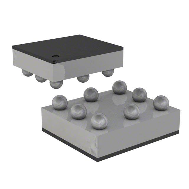


 工商网监
湘ICP备2023018690号
工商网监
湘ICP备2023018690号
