STGB18N40LZT4
Datasheet
Automotive-grade 390 V internally clamped IGBT ESCIS 180 mJ
Features
TAB
3
1
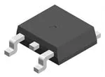
D2PAK
C (2 or TAB)
AEC-Q101 qualified
SCIS energy of 180 mJ @ TC = 150 °C, L = 3 mH
•
•
•
•
•
•
•
Parts are 100% tested in SCIS
ESD gate-emitter protection
Gate-collector high voltage clamping
Logic level gate drive
Very low saturation voltage
High pulsed current capability
Gate and gate-emitter resistor
Applications
RG
G (1)
•
•
•
Pencil coil electronic ignition driver
RGE
Description
E (3)
IGBTG1C2TABE3ESD
This application-specific IGBT utilizes the most advanced PowerMESH technology
optimized for coil driving in the harsh environment of automotive ignition systems.
The device show very low on-state voltage and very high SCIS energy capability over
a wide operating temperature range. Moreover, ESD-protected logic level gate input
and an integrated gate resistor means no external protection circuitry is required.
Product status link
STGB18N40LZT4
Product summary
Order code
STGB18N40LZT4
Marking
GB18N40LZ
Package
D²PAK
Packing
Tape and reel
DS5664 - Rev 7 - January 2021
For further information contact your local STMicroelectronics sales office.
www.st.com
�STGB18N40LZT4
Electrical ratings
1
Electrical ratings
Table 1. Absolute maximum ratings
Symbol
Parameter
Value
Unit
VCES
Collector-emitter voltage (VGE = 0 V)
VCES(clamped)
V
VECS
Emitter-collector voltage (VGE = 0 V)
20
V
Continuous collector current at TC = 100 °C
30
A
Pulsed collector current
40
A
VGE(clamped)
V
IC
ICP
(1)
VGE
Gate-emitter voltage
PTOT
Total power dissipation at TC = 25 °C
150
W
Single pulse energy TC = 25 °C, L = 3 mH, VCC = 50 V
300
mJ
Single pulse energy TC = 150 °C, L = 3 mH, VCC = 50 V
180
mJ
ESCIS (2)
Human body model, R = 1.5 kΩ, C = 100 pF
ESD
Machine model, R = 0, C = 100 pF
Charged device model
TSTG
TJ
Storage temperature range
Operating junction temperature range
8
kV
800
V
2
kV
-55 to 175
°C
°C
1. Pulse width limited by max. junction temperature.
2. For ESCIS test circuit refer to Figure 14. Test circuit for inductive load switching with A and B not connected.
Table 2. Thermal data
Symbol
DS5664 - Rev 7
Parameter
RthJC
Thermal resistance, junction-to-case
RthJA
Thermal resistance, junction-to-ambient
Value
Unit
1
°C/W
62.5
°C/W
page 2/16
�STGB18N40LZT4
Electrical characteristics
2
Electrical characteristics
TC = 25 °C unless otherwise specified
Table 3. Static characteristics
Symbol
Parameter
Test conditions
VCES(clamped)
Collector-emitter clamped voltage
IC = 2 mA, VGE = 0 V,
TJ= - 40 °C to 175 °C
Min.
Typ.
Max.
Unit
360
390
420
V
28
V(BR)ECS
Emitter-collector break-down
voltage
VGE = 0 V, IC = 75 mA
20
VGE(clamped)
Gate-emitter clamped voltage
IG = ±2 mA
12
VGE = 4.5 V, IC = 10 A
VCE(sat)
Collector-emitter saturation
voltage
1.35
VGE = 4.5 V, IC = 10 A,
TJ = 150 °C
VGE = 3.8 V, IC = 6 A
VGE(th)
Gate-threshold voltage
VGE = VCE, IC = 1 mA,
TJ = -40 °C
1.4
VGE = VCE, IC = 1 mA
1.2
VGE = VCE, IC = 1 mA,
TJ = 150 °C (1)
0.7
RGE
Gate emitter resistance
RG
Gate resistance
VGE = ±10 V, VCE = 0 V
V
V
V
1.6
2.3
V
V
TJ = 150 °C (1)
Gate-emitter leakage current
1.7
1.30
VCE = 200 V, VGE = 0 V,
IGES
V
V
TJ = 150 °C (1)
Collector cut-off current
16
1.30
VCE = 15 V, VGE = 0 V,
ICES
V
10
µA
100
µA
450
625
830
µA
12
16
22
kΩ
1.6
kΩ
1. Defined by design, not subject to production test.
Table 4. Dynamic characteristics
Symbol
Cies
Input capacitance
Coes
Output capacitance
Cres
Reverse transfer capacitance
Qg
DS5664 - Rev 7
Parameter
Total gate charge
Test conditions
VCE = 25 V, f = 1 MHz,
VGE = 0 V
VCE = 280 V, IC = 10 A,
VGE = 0 to 5 V
Min.
Typ.
Max.
-
490
-
-
90
-
-
5
-
-
29
-
Unit
pF
nC
page 3/16
�STGB18N40LZT4
Electrical characteristics
Table 5. Resistive load switching characteristics
Symbol
td(on)
tr
td(on)
tr
Parameter
Test conditions
Min.
Typ.
Max.
Unit
Turn-on delay time
VCC = 14 V, VGE = 5 V,
-
0.65
-
μs
Current rise time
RL = 1 Ω
-
3.5
-
μs
Turn-on delay time
VCC = 14 V, VGE = 5 V,
-
0.65
-
μs
Current rise time
RL= 1 Ω, TJ = 150 °C
-
3.8
-
μs
Min.
Typ.
Max.
Unit
-
13.5
-
μs
-
5.5
-
μs
-
105
-
V/μs
Table 6. Inductive load switching characteristics
Symbol
td(off)
tf
Turn-off delay time
Current fall time
Test conditions
VCC = 300 V, L = 1 mH,
IC = 10 A, VGE = 5 V,
dV/dt
Turn-off voltage slope
td(off)
Turn-off delay time
VCC = 300 V, L = 1 mH,
-
14.2
-
μs
Current fall time
IC = 10 A, VGE = 5 V,
TJ = 150 °C
-
8
-
μs
-
97
-
V/μs
tf
dV/dt
DS5664 - Rev 7
Parameter
Turn-off voltage slope
page 4/16
�STGB18N40LZT4
Electrical characteristics (curves)
2.1
Electrical characteristics (curves)
Figure 1. Collector-emitter on voltage vs temperature
Figure 2. Collector-emitter on voltage vs temperature
Figure 3. Collector-emitter on voltage vs temperature
Figure 4. Self clamped inductive switch
AM03942v1
IS CIS
(A)
VGE =5V
VCE =50V
24
16
TJ =25°C
8
TJ =150°C
0
Figure 5. Output characteristics at 25 °C
HV42380
60
IC (A)
VGE = 5 V
6
→
VGE = 4 V
VGE = 3 .8 V
30
20
HV42390
VGE = 8 V
VGE = 4.5 V
VGE = 5 V
VGE = 4 V
40
VGE = 3.8 V
30
20
TC = -40 °C
T C = 25 °C
10
DS5664 - Rev 7
L(mH)
IC (A)
60
50
40
0
8
Figure 6. Output characteristics at -40 °C
VGE = 4.5 V
VGE = 8 V
50
4
2
0
10
0
1
2
3
4
5
0
VCE (V)
0
1
2
3
4
5 VCE (V)6
page 5/16
�STGB18N40LZT4
Electrical characteristics (curves)
Figure 7. Output characteristics at 175 °C
HV42400
60
IC (A)
VGE = 5 V
VGE = 8 V
Figure 8. Transfer characteristics
HV38710
40
IC (A)
35
50
VGE = 4.5 V
40
VGE = 4 V
25
30
VGE = 3.8 V
20
VCE= 5V
30
15
20
175°C
10
TC = 175 °C
10
25°C
5
-40°C
0
0
0
1
2
3
4
5 VCE (V)6
1.0
1.5
2.0
2.5
3.0
3.5
4.0
GE (V)
4.5 V5.0
Figure 9. Collector cut-off current vs temperature
Figure 10. Normalized collector emitter voltage vs
temperature
Figure 11. Normalized gate threshold voltage vs
temperature
Figure 12. Normalized collector emitter on voltage vs
temperature
DS5664 - Rev 7
page 6/16
�STGB18N40LZT4
Electrical characteristics (curves)
Figure 13. Thermal impedance
DS5664 - Rev 7
page 7/16
�STGB18N40LZT4
Test circuits
3
Test circuits
Figure 14. Test circuit for inductive load switching
Figure 15. Test circuit for resistive load switching
A
C
A
L=100 µH
G
L
E
B
B
G
+
3.3
µF
C
VCC
1000
µF
D.U.T
RG
E
AM01504v2
AM01504v1
Figure 17. Switching waveform
Figure 16. Gate charge test circuit
k
k
90%
10%
VG
90%
VCE
k
10%
tr(Voff)
tcross
90%
k
IC
k
td(on)
ton
td(off)
tr(Ion)
10%
tf
toff
k
AM01505v1
AM01506v1
DS5664 - Rev 7
page 8/16
�STGB18N40LZT4
Package information
4
Package information
In order to meet environmental requirements, ST offers these devices in different grades of ECOPACK packages,
depending on their level of environmental compliance. ECOPACK specifications, grade definitions and product
status are available at: www.st.com. ECOPACK is an ST trademark.
4.1
D²PAK (TO-263) type A package information
Figure 18. D²PAK (TO-263) type A package outline
0079457_26
DS5664 - Rev 7
page 9/16
�STGB18N40LZT4
D²PAK (TO-263) type A package information
Table 7. D²PAK (TO-263) type A package mechanical data
Dim.
mm
Min.
Max.
A
4.40
4.60
A1
0.03
0.23
b
0.70
0.93
b2
1.14
1.70
c
0.45
0.60
c2
1.23
1.36
D
8.95
9.35
D1
7.50
7.75
8.00
D2
1.10
1.30
1.50
E
10.00
E1
8.30
8.50
8.70
E2
6.85
7.05
7.25
e
10.40
2.54
e1
4.88
5.28
H
15.00
15.85
J1
2.49
2.69
L
2.29
2.79
L1
1.27
1.40
L2
1.30
1.75
R
V2
DS5664 - Rev 7
Typ.
0.40
0°
8°
page 10/16
�STGB18N40LZT4
D²PAK (TO-263) type A package information
Figure 19. D²PAK (TO-263) recommended footprint (dimensions are in mm)
Footprint_26
DS5664 - Rev 7
page 11/16
�STGB18N40LZT4
D²PAK packing information
4.2
D²PAK packing information
Figure 20. D²PAK tape outline
DS5664 - Rev 7
page 12/16
�STGB18N40LZT4
D²PAK packing information
Figure 21. D²PAK reel outline
T
40mm min.
access hole
at slot location
B
D
C
N
A
G measured
at hub
Tape slot
in core for
tape start
2.5mm min.width
Full radius
AM06038v1
Table 8. D²PAK tape and reel mechanical data
Tape
Dim.
DS5664 - Rev 7
Reel
mm
mm
Dim.
Min.
Max.
Min.
Max.
A0
10.5
10.7
A
B0
15.7
15.9
B
1.5
D
1.5
1.6
C
12.8
D1
1.59
1.61
D
20.2
E
1.65
1.85
G
24.4
F
11.4
11.6
N
100
K0
4.8
5.0
T
P0
3.9
4.1
P1
11.9
12.1
Base quantity
1000
P2
1.9
2.1
Bulk quantity
1000
R
50
T
0.25
0.35
W
23.7
24.3
330
13.2
26.4
30.4
page 13/16
�STGB18N40LZT4
Revision history
Table 9. Document revision history
Date
Revision
Changes
18-Jan-2008
1
Initial release.
07-Mar-2008
2
Modified Figure 7, Figure 8, Figure 10.
07-May-2008
3
Modified Figure 9
31-Mar-2009
4
Added new package, mechanical data: TO-220
18-May-2009
5
Modified Figure 5
Updated Table 1: Device summary, Table 2: Absolute maximum
ratings and Table 3: Thermal data
12-Nov-2014
6
Updated 3: Test circuits
Updated Section 4: Package mechanical data
Updated Section 5: Packaging mechanical data
Minor text changes
11-Jan-2021
DS5664 - Rev 7
7
The part numbers STGD18N40LZ and STGP18N40LZT4 have been removed.
Minor text changes
page 14/16
�STGB18N40LZT4
Contents
Contents
1
Electrical ratings . . . . . . . . . . . . . . . . . . . . . . . . . . . . . . . . . . . . . . . . . . . . . . . . . . . . . . . . . . . . . . . . . .2
2
Electrical characteristics. . . . . . . . . . . . . . . . . . . . . . . . . . . . . . . . . . . . . . . . . . . . . . . . . . . . . . . . . . . 3
2.1
Electrical characteristics (curves). . . . . . . . . . . . . . . . . . . . . . . . . . . . . . . . . . . . . . . . . . . . . . . . . 5
3
Test circuits . . . . . . . . . . . . . . . . . . . . . . . . . . . . . . . . . . . . . . . . . . . . . . . . . . . . . . . . . . . . . . . . . . . . . . .8
4
Package information. . . . . . . . . . . . . . . . . . . . . . . . . . . . . . . . . . . . . . . . . . . . . . . . . . . . . . . . . . . . . . .9
4.1
D²PAK (TO-263) type A package information . . . . . . . . . . . . . . . . . . . . . . . . . . . . . . . . . . . . . . . 9
4.2
D²PAK packing information . . . . . . . . . . . . . . . . . . . . . . . . . . . . . . . . . . . . . . . . . . . . . . . . . . . . . 12
Revision history . . . . . . . . . . . . . . . . . . . . . . . . . . . . . . . . . . . . . . . . . . . . . . . . . . . . . . . . . . . . . . . . . . . . . . .14
DS5664 - Rev 7
page 15/16
�STGB18N40LZT4
IMPORTANT NOTICE – PLEASE READ CAREFULLY
STMicroelectronics NV and its subsidiaries (“ST”) reserve the right to make changes, corrections, enhancements, modifications, and improvements to ST
products and/or to this document at any time without notice. Purchasers should obtain the latest relevant information on ST products before placing orders. ST
products are sold pursuant to ST’s terms and conditions of sale in place at the time of order acknowledgement.
Purchasers are solely responsible for the choice, selection, and use of ST products and ST assumes no liability for application assistance or the design of
Purchasers’ products.
No license, express or implied, to any intellectual property right is granted by ST herein.
Resale of ST products with provisions different from the information set forth herein shall void any warranty granted by ST for such product.
ST and the ST logo are trademarks of ST. For additional information about ST trademarks, please refer to www.st.com/trademarks. All other product or service
names are the property of their respective owners.
Information in this document supersedes and replaces information previously supplied in any prior versions of this document.
© 2021 STMicroelectronics – All rights reserved
DS5664 - Rev 7
page 16/16
�