STGD10NC60SD
STGF10NC60SD
10 A, 600 V fast IGBT
Features
Optimized performance for medium operating
frequencies up to 5 kHz in hard switching
■
Low on-voltage drop (VCE(sat))
■
Very soft ultra fast antiparallel diode
TA
B
■
3
Application
■
3
1
Motor drive
DPAK
1
2
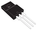
TO-220FP
Description
This IGBT utilizes the advanced PowerMESH™
process resulting in an excellent trade-off
between switching performance and low on-state
behavior.
Table 1.
Figure 1.
Internal schematic diagram
Device summary
Order codes
Marking
Package
Packaging
STGD10NC60SDT4
GD10NC60SD
DPAK
Tape and reel
STGF10NC60SD
GF10NC60SD
TO-220FP
Tube
June 2010
Doc ID 15847 Rev 2
1/16
www.st.com
16
�Contents
STGD10NC60SD, STGF10NC60SD
Contents
1
Electrical ratings . . . . . . . . . . . . . . . . . . . . . . . . . . . . . . . . . . . . . . . . . . . . 3
2
Electrical characteristics . . . . . . . . . . . . . . . . . . . . . . . . . . . . . . . . . . . . . 4
2.1
Electrical characteristics (curves) . . . . . . . . . . . . . . . . . . . . . . . . . . . . . . . . 6
3
Test circuits
4
Package mechanical data . . . . . . . . . . . . . . . . . . . . . . . . . . . . . . . . . . . . 10
5
Packaging mechanical data . . . . . . . . . . . . . . . . . . . . . . . . . . . . . . . . . . 14
6
Revision history . . . . . . . . . . . . . . . . . . . . . . . . . . . . . . . . . . . . . . . . . . . 15
2/16
............................................... 9
Doc ID 15847 Rev 2
�STGD10NC60SD, STGF10NC60SD
1
Electrical ratings
Electrical ratings
Table 2.
Absolute maximum ratings
Value
Symbol
DPAK
VCES
IC
(1)
IC(1)
Collector-emitter voltage (VGE = 0)
TO-220FP
600
V
Continuous collector current at TC = 25°C
18
10
A
Continuous collector current at TC = 100°C
10
5
A
ICL
(2)
Turn-off latching current
14
A
ICP
(3)
Pulsed collector current
25
A
Diode RMS forward current at TC=25 °C
10
A
IFSM
Surge non repetitive forward current tp = 10 ms
sinusoidal
20
A
VGE
Gate-emitter voltage
±20
V
PTOT
Total dissipation at TC = 25 °C
VISO
Isolation withstand voltage (RMS) from all three leads
to external heat sink (t = 1 sec; TC = 25 °C)
IF
Tj
1.
Unit
Parameter
60
Operating junction temperature
25
W
2500
V
-55 to 150
°C
Calculated according to the iterative formula:
T j ( max ) – T C
I C ( T C ) = --------------------------------------------------------------------------------------------------------R thj – c × V CE ( sat ) ( max ) ( T j ( max ), I C ( T C ) )
2. Vclamp = 80%,(VCES), Tj =150 °C, RG = 10 Ω, VGE = 15 V.
3. Pulse width limited by maximum junction temperature and turn-off within RBSOA.
Table 3.
Thermal data
Value
Symbol
Parameter
Thermal resistance junction-case IGBT
Rthj-case
Rthj-amb
Unit
DPAK
TO-220FP
2.08
5
Thermal resistance junction-case diode
Thermal resistance junction-ambient
Doc ID 15847 Rev 2
4.5
100
°C/W
°C/W
62.5
°C/W
3/16
�Electrical characteristics
2
STGD10NC60SD, STGF10NC60SD
Electrical characteristics
(TJ=25°C unless otherwise specified)
Table 4.
Symbol
Parameter
Test conditions
V(BR)CES
Collector-emitter breakdown
IC= 1 mA
voltage (VGE= 0)
VCE(sat)
Collector-emitter saturation
voltage
VGE= 15 V, IC= 5 A
VGE= 15 V, IC= 5 A, TJ= 125 °C
VGE(th)
Gate threshold voltage
VCE= VGE, IC= 250 µA
ICES
Collector cut-off current
(VGE=0)
IGES
gfs
Table 5.
Symbol
4/16
Static
Min.
Typ.
Max. Unit
600
V
1.45
1.45
1.65
V
V
5.75
V
VCE= 600 V
VCE=600 V, TJ=125 °C
150
1
µA
mA
Gate-emitter leakage
(VCE=0)
VGE= ±20 V
±100
nA
Forward transconductance
VCE = 15 V , IC = 5 A
3.75
3.5
S
Dynamic
Parameter
Test conditions
Min.
Typ.
Max.
Unit
Cies
Coes
Cres
Input capacitance
Output capacitance
Reverse transfer
capacitance
VCE = 25 V, f = 1 MHz, VGE= 0
-
365
44
8
-
pF
pF
pF
Qg
Qge
Qgc
Total gate charge
Gate-emitter charge
Gate-collector charge
VCE = 480 V, IC = 5 A,
VGE = 15 V
Figure 18
-
18
8
3.5
-
nC
nC
nC
Doc ID 15847 Rev 2
�STGD10NC60SD, STGF10NC60SD
Table 6.
Electrical characteristics
Switching on/off (inductive load)
Symbol
Parameter
Test conditions
Min.
Typ.
td(on)
tr
(di/dt)on
Turn-on delay time
Current rise time
Turn-on current slope
td(on)
tr
(di/dt)on
VCC = 390 V, IC = 5 A
RG= 10 Ω, VGE= 15 V,
Figure 19
-
19
4
1330
-
ns
ns
A/µs
Turn-on delay time
Current rise time
Turn-on current slope
VCC = 390 V, IC = 5 A
RG= 10 Ω, VGE= 15 V,
TJ= 125°C
Figure 19
-
18
4.5
1000
-
ns
ns
A/µs
tr(Voff)
td(off)
tf
Off voltage rise time
Turn-off delay time
Current fall time
Vcc = 390 V, IC = 5 A,
RG = 10 Ω, VGE = 15 V,
Figure 19
-
100
160
205
-
ns
ns
ns
tr(Voff)
td(off)
tf
Off voltage rise time
Turn-off delay time
Current fall time
Vcc = 390 V, IC = 5 A,
RG = 10 Ω, VGE = 15 V,
TJ = 125°C
Figure 19
-
165
250
310
-
ns
ns
ns
Min.
Typ.
Max.
Unit
Table 7.
Symbol
Max. Unit
Switching energy (inductive load)
Parameter
Test conditions
Eon (1)
Eoff (2)
Ets
Turn-on switching losses
Turn-off switching losses
Total switching losses
VCC = 480 V, IC = 5 A
RG= 10 Ω, VGE= 15 V,
Figure 17
-
60
340
400
-
µJ
µJ
µJ
Eon (1)
Eoff(2)
Ets
Turn-on switching losses
Turn-off switching losses
Total switching losses
VCC = 480 V, IC = 5 A
RG= 10 Ω, VGE= 15 V,
TJ= 125°C
Figure 17
-
90
540
630
-
µJ
µJ
µJ
1. Eon is the turn-on losses when a typical diode is used in the test circuit in Figure 17. If the IGBT is offered
in a package with a co-pack diode, the co-pack diode is used as external diode. IGBTs and diode are at the
same temperature.
2. Turn-off losses included also include also the tail of the collector current.
Table 8.
Symbol
Collector-emitter diode
Parameter
Test conditions
Min.
Typ.
Max.
Unit
-
2
1.65
2.45
V
V
ns
nC
A
ns
nC
A
VF
Forward on-voltage
IF=5 A
IF=5 A, TJ=125 °C
trr
Qrr
Irrm
Reverse recovery time
Reverse recovery charge
Reverse recovery current
IF=5 A, VR=40 V,
di/dt=100 A/µs
Figure 20
-
22
14
1.3
trr
Qrr
Irrm
Reverse recovery time
Reverse recovery charge
Reverse recovery current
IF=5 A, VR=40 V,
TJ=125 °C, di/dt=100 A/µs
Figure 20
-
34
35
2.1
Doc ID 15847 Rev 2
5/16
�Electrical characteristics
STGD10NC60SD, STGF10NC60SD
2.1
Electrical characteristics (curves)
Figure 2.
Output characteristics
Figure 3.
AM07263v1
30
IC (A)
AM07262v1
IC 30
(A)
Transfer characteristics
VGE = 15 V
VGE = 11 V
25
20
25
20
VGE = 10 V
VCE = 10 V
15
15
VGE = 9 V
10
10
VGE = 8 V
5
5
VGE = 7 V
0
0
0
Figure 4.
2
4
6
8
VCE 10
(V)
Collector-emitter on voltage vs
collector current
AM07264v1
VCE(sat)
3
(V)
0
Figure 5.
4
TJ = 25 ºC
6
8
10 VGE 12
(V)
Collector-emitter on voltage vs
temperature
AM08265v1
VCE(sat)
2
(V)
TJ = 150 ºC
2.5
2
IC = 10 A
1.8
VGE = 15 V
1.6
2
TJ = -50 ºC
IC = 5 A
1.4
1.5
VGE = 15 V
1.2
1
1
0.5
0
Figure 6.
IC = 2.5 A
4
8
12
16
IC 20
(A)
Normalized breakdown voltage vs
temperature
Figure 7.
0
50
100
TJ (ºC)
Normalized gate threshold vs
temperature
VGE(th)
(norm)
AM07266v1
V1.15
CES
(norm)
-50
AM07267V1
1.1
1.1
IC = 1 mA
1
1.05
0.9
1
0.8
0.95
0.7
0.6
0.9
-50
6/16
VGE = VCE
IC = 250 µA
0
50
100
TJ 150
(ºC)
Doc ID 15847 Rev 2
-50
0
50
100
TJ (°C)
�STGD10NC60SD, STGF10NC60SD
Figure 8.
Electrical characteristics
Capacitance variations
Figure 9.
AM07269v1
Gate charge vs gate-emitter voltage
AM07268v1
VGE (V)
20
C (pF)
f = 1 MHz
VGE = 0
VCC = 480 V
IC = 5 A
16
600
12
Cies
400
8
200
4
Coes
Cres
0
0
0
10
20
30
VCE
40
Figure 10. Switching losses vs temperature
0
12
16
QG (nC)
AM07271v1
E 600
(µJ)
500
500
EOFF
400
8
Figure 11. Switching losses vs gate resistance
AM07270v1
E600
(µJ)
4
EOFF
400
300
VCC = 480 V, VGE= 15 V
I C = 5 A, TJ = 125 °C
300
VCC = 480 V, VGE= 15 V
I C = 5 A, RG =10 Ω
200
200
EON
EON
100
100
0
0
25
50
75
100
TJ (°C)
Figure 12. Switching losses vs collector
current
0
40
80
120
160
RG (Ω)
200
Figure 13. Diode forward on voltage
AM07272v1
E (µJ)
)&-�!
VCC = 480 V, VGE= 15 V
RG =10 Ω, TJ = 125 °C
500
400
��
��
��
��
��
��
�
�
�
�
�
�
�
�
�
�
EOFF
300
200
EON
100
0
1
2
3
4
IC (A)
4J���� #
�MAXIMUMVALUES
4J��� #
�MAXIMUMVALUES
4J���� #
�TYPICALVALUES
6&-�6
�
Doc ID 15847 Rev 2
�
�
�
�
�
7/16
�Electrical characteristics
STGD10NC60SD, STGF10NC60SD
Figure 14. Thermal impedance for DPAK
+
Figure 15. Thermal impedance for TO-220FP
+
K�����
K�����
���
���
�
���
��
���
?YM " P 7YM/ªH
K " YU �[
�
��
?YM " P 7YM/ªH
K " YU �[
����
����
�
��
����
����
�
��
�
��
YU
[
3INGLEPULSE
�
��
�
�
�
��
��
�
��
TP �S
��
�
��
Figure 16. Turn-off SOA
AM07273V1
IC
(A)
10
1
0.1
0.01
0.1
8/16
1
10
����
����
100
VCE(V)
Doc ID 15847 Rev 2
YU
[
3INGLEPULSE
�
��
�
��
�
��
�
��
TP �S
�STGD10NC60SD, STGF10NC60SD
3
Test circuits
Test circuits
Figure 17. Test circuit for inductive load
switching
Figure 18. Gate charge test circuit
Figure 19. Switching waveforms
Figure 20. Diode recovery time waveform
Doc ID 15847 Rev 2
9/16
�Package mechanical data
4
STGD10NC60SD, STGF10NC60SD
Package mechanical data
In order to meet environmental requirements, ST offers these devices in different grades of
ECOPACK® packages, depending on their level of environmental compliance. ECOPACK®
specifications, grade definitions and product status are available at: www.st.com.
ECOPACK is an ST trademark.
10/16
Doc ID 15847 Rev 2
�STGD10NC60SD, STGF10NC60SD
Package mechanical data
TO-252 (DPAK) mechanical data
DIM.
mm.
min.
typ
max.
A
2.20
2.40
A1
0.90
1.10
A2
0.03
0.23
b
0.64
0.90
b4
5.20
5.40
c
0.45
0.60
c2
0.48
0.60
D
6.00
6.20
D1
E
5.10
6.40
6.60
E1
4.70
e
2.28
e1
4.40
4.60
H
9.35
10.10
L
1
L1
2.80
L2
L4
0.80
0.60
1
R
V2
0.20
8o
0o
0068772_G
Doc ID 15847 Rev 2
11/16
�Package mechanical data
Table 9.
STGD10NC60SD, STGF10NC60SD
TO-220FP mechanical data
mm
Dim.
Min.
Typ.
A
4.4
4.6
B
2.5
2.7
D
2.5
2.75
E
0.45
0.7
F
0.75
1
F1
1.15
1.70
F2
1.15
1.70
G
4.95
5.2
G1
2.4
2.7
H
10
10.4
L2
12/16
Max.
16
L3
28.6
30.6
L4
9.8
10.6
L5
2.9
3.6
L6
15.9
16.4
L7
9
9.3
Dia
3
3.2
Doc ID 15847 Rev 2
�STGD10NC60SD, STGF10NC60SD
Package mechanical data
Figure 21. TO-220FP drawing
L7
E
A
B
D
Dia
L5
L6
F1
F2
F
G
H
G1
L4
L2
L3
7012510_Rev_K
Doc ID 15847 Rev 2
13/16
�Packaging mechanical data
5
STGD10NC60SD, STGF10NC60SD
Packaging mechanical data
DPAK FOOTPRINT
All dimensions are in millimeters
TAPE AND REEL SHIPMENT
REEL MECHANICAL DATA
DIM.
mm
MIN.
A
B
1.5
C
12.8
D
20.2
G
16.4
N
50
T
TAPE MECHANICAL DATA
DIM.
mm
MIN.
MAX.
A0
6.8
7
0.267 0.275
B0
10.4
10.6
0.409 0.417
B1
D
14/16
inch
1.5
D1
1.5
E
1.65
MIN.
MAX.
12.1
0.476
1.6
0.059 0.063
1.85
0.065 0.073
0.059
F
7.4
7.6
0.291 0.299
K0
2.55
2.75
0.100 0.108
0.153 0.161
P0
3.9
4.1
P1
7.9
8.1
0.311 0.319
P2
1.9
2.1
0.075 0.082
R
40
W
15.7
1.574
16.3
0.618
0.641
Doc ID 15847 Rev 2
inch
MAX.
MIN.
MAX.
330
12.992
13.2
0.504 0.520
18.4
0.645 0.724
0.059
0.795
1.968
22.4
0.881
BASE QTY
BULK QTY
2500
2500
�STGD10NC60SD, STGF10NC60SD
6
Revision history
Revision history
Table 10.
Document revision history
Date
Revision
Changes
06-Jul-2009
1
Initial release
14-Jun-2010
2
Inserted Section 2.1: Electrical characteristics (curves).
Doc ID 15847 Rev 2
15/16
�STGD10NC60SD, STGF10NC60SD
Please Read Carefully:
Information in this document is provided solely in connection with ST products. STMicroelectronics NV and its subsidiaries (“ST”) reserve the
right to make changes, corrections, modifications or improvements, to this document, and the products and services described herein at any
time, without notice.
All ST products are sold pursuant to ST’s terms and conditions of sale.
Purchasers are solely responsible for the choice, selection and use of the ST products and services described herein, and ST assumes no
liability whatsoever relating to the choice, selection or use of the ST products and services described herein.
No license, express or implied, by estoppel or otherwise, to any intellectual property rights is granted under this document. If any part of this
document refers to any third party products or services it shall not be deemed a license grant by ST for the use of such third party products
or services, or any intellectual property contained therein or considered as a warranty covering the use in any manner whatsoever of such
third party products or services or any intellectual property contained therein.
UNLESS OTHERWISE SET FORTH IN ST’S TERMS AND CONDITIONS OF SALE ST DISCLAIMS ANY EXPRESS OR IMPLIED
WARRANTY WITH RESPECT TO THE USE AND/OR SALE OF ST PRODUCTS INCLUDING WITHOUT LIMITATION IMPLIED
WARRANTIES OF MERCHANTABILITY, FITNESS FOR A PARTICULAR PURPOSE (AND THEIR EQUIVALENTS UNDER THE LAWS
OF ANY JURISDICTION), OR INFRINGEMENT OF ANY PATENT, COPYRIGHT OR OTHER INTELLECTUAL PROPERTY RIGHT.
UNLESS EXPRESSLY APPROVED IN WRITING BY AN AUTHORIZED ST REPRESENTATIVE, ST PRODUCTS ARE NOT
RECOMMENDED, AUTHORIZED OR WARRANTED FOR USE IN MILITARY, AIR CRAFT, SPACE, LIFE SAVING, OR LIFE SUSTAINING
APPLICATIONS, NOR IN PRODUCTS OR SYSTEMS WHERE FAILURE OR MALFUNCTION MAY RESULT IN PERSONAL INJURY,
DEATH, OR SEVERE PROPERTY OR ENVIRONMENTAL DAMAGE. ST PRODUCTS WHICH ARE NOT SPECIFIED AS "AUTOMOTIVE
GRADE" MAY ONLY BE USED IN AUTOMOTIVE APPLICATIONS AT USER’S OWN RISK.
Resale of ST products with provisions different from the statements and/or technical features set forth in this document shall immediately void
any warranty granted by ST for the ST product or service described herein and shall not create or extend in any manner whatsoever, any
liability of ST.
ST and the ST logo are trademarks or registered trademarks of ST in various countries.
Information in this document supersedes and replaces all information previously supplied.
The ST logo is a registered trademark of STMicroelectronics. All other names are the property of their respective owners.
© 2010 STMicroelectronics - All rights reserved
STMicroelectronics group of companies
Australia - Belgium - Brazil - Canada - China - Czech Republic - Finland - France - Germany - Hong Kong - India - Israel - Italy - Japan Malaysia - Malta - Morocco - Philippines - Singapore - Spain - Sweden - Switzerland - United Kingdom - United States of America
www.st.com
16/16
Doc ID 15847 Rev 2
�