STGF20NB60S
PowerMESH™ IGBT, S series
600 V, 13 A low drop
Datasheet - production data
Features
Low on-voltage drop (VCE(sat))
High current capability
Applications
3
1
2
Light dimmer
Static relays
Motor control
Description
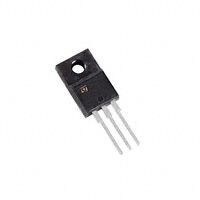
TO-220FP
Using the latest high voltage technology based
on a patented strip layout, STMicroelectronics
has designed an advanced family of IGBTs, the
PowerMESH™ IGBTs, with outstanding
performance. The suffix “S” represents a series
optimized to achieve minimum on-voltage drop
for low frequency applications.
Figure 1: Internal schematic diagram
Table 1: Device summary
Order code
Marking
Package
Packing
STGF20NB60S
GF20NB60S
TO-220FP
Tube
December 2015
DocID9910 Rev 4
This is information on a product in full production.
1/14
www.st.com
�Contents
STGF20NB60S
Contents
1
Electrical ratings ............................................................................. 3
2
Electrical characteristics ................................................................ 4
2.1
Electrical characteristics (curves) ...................................................... 6
3
Test circuits ..................................................................................... 9
4
Package information ..................................................................... 10
4.1
5
2/14
TO-220FP package information ...................................................... 11
Revision history ............................................................................ 13
DocID9910 Rev 4
�STGF20NB60S
1
Electrical ratings
Electrical ratings
Table 2: Absolute maximum ratings
Symbol
Parameter
Value
Unit
VCES
Collector-emitter voltage (VGE = 0 V)
600
V
VECS
Emitter-collector voltage (VGE = 0 V)
-20
V
VGE
Gate-emitter voltage
±20
V
Continuous collector current at TC = 25 °C
24
Continuous collector current at TC = 100 °C
13
ICL
Turn-off latching current
70
A
ICM(1)
Pulsed collector current
70
A
PTOT
Total dissipation at TC = 25 °C
40
W
VISO
Insulation withstand voltage (RMS) from all three leads to
external heat sink (t = 1 s, TC = 25 °C)
2.5
kV
TSTG
Storage temperature range
-55 to 150
°C
Value
Unit
IC
TJ
Operating junction temperature
A
Notes:
(1)Pulse
width limited by safe operating area.
Table 3: Thermal data
Symbol
Parameter
Rthj-case
Thermal resistance junction-case
3.1
Rthj-amb
Thermal resistance junction-ambient
62.5
DocID9910 Rev 4
°C/W
3/14
�Electrical characteristics
2
STGF20NB60S
Electrical characteristics
TC = 25 °C unless otherwise specified
Table 4: Static characteristics
Symbol
Parameter
Test conditions
Min.
V(BR)CES
Collector-emitter breakdown
voltage
VGE = 0 V, IC = 250 µA
600
V(BR)ECS
Emitter-collector breakdown
voltage
VGE = 0 V, IC = 10 mA
Typ.
Max.
Unit
V
-20
VGE = 0 V, VCE = 600 V
10
ICES
Collector cut-off current
VGE = 0 V, VCE = 600 V,
TC = 125 °C
100
IGES
Gate-emitter leakage current
VCE = 0 V, VGE = ±20 V
±100
nA
VGE(th)
Gate threshold voltage
VCE = VGE, IC = 250 µA
5
V
VCE(sat)
Collector-emitter saturation
voltage
2.5
VGE = 15 V, IC = 20 A
1.25
VGE = 15 V, IC = 20 A,
TJ = 150 °C
1.2
µA
1.7
V
Table 5: Dynamic characteristics
Symbol
Parameter
Test conditions
gfs(1)
Forward transconductance
Cies
Input capacitance
Coes
Output capacitance
Cres
Reverse transfer
capacitance
Qg
Total gate charge
Qge
Gate-emitter charge
Qgc
Gate-collector charge
VCE = 10 V, IC = 8 A
VCE= 25 V, f = 1 MHz,
VGE = 0 V
VCC = 480 V, IC = 20 A,
VGE = 15 V (see Figure 17:
"Gate charge test circuit")
Min.
Typ.
Max.
Unit
-
20
-
S
-
1820
-
-
167
-
-
27
-
-
83
115
-
10
-
-
27
-
pF
nC
Notes:
(1)Pulse
duration= 300 μs, duty cycle 1.5 %
Table 6: Inductive load switching on characteristics
Symbol
td(on)
tr
(di/dt)on
td(on)
tr
(di/dt)on
4/14
Parameter
Turn-on delay time
Current rise time
Turn-on current slope
Turn-on delay time
Current rise time
Turn-on current slope
Test conditions
Min.
Typ.
Max.
Unit
VCC = 480 V, IC = 20 A,
VGE = 15 V, RG = 100 Ω
(see Figure 16: "Test circuit
for inductive load switching")
-
92
-
ns
-
70
-
ns
-
340
-
A/µs
VCC = 480 V, IC = 20 A,
VGE = 15 V, RG = 100 Ω,
Tj = 125 °C (see Figure 16:
"Test circuit for inductive load
switching")
-
80
-
ns
-
73
-
ns
-
320
-
A/µs
DocID9910 Rev 4
�STGF20NB60S
Electrical characteristics
Table 7: Inductive load switching off characteristics
Symbol
tc
Parameter
Cross-over time
tr(Voff)
Off voltage rise time
td(off)
Turn-off delay time
tf
Current fall time
tc
Cross-over time
tr(Voff)
Off voltage rise time
td(off)
Turn-off delay time
tf
Current fall time
Test conditions
Min.
Typ.
Max.
-
1.6
-
-
0.8
-
-
1.1
-
-
0.8
-
-
2.4
-
-
1.1
-
-
2.4
-
-
1.2
-
Min.
Typ.
Max.
VCC = 480 V, IC = 20 A,
VGE = 15 V, RG = 100 Ω
(see Figure 18: "Switching
waveform")
-
0.84
-
-
7.4
-
-
8.24
-
VCC = 480 V, IC = 20 A,
VGE = 15 V, RG = 100 Ω,
Tj = 125 °C (see Figure 18:
"Switching waveform")
-
0.86
-
-
11.5
-
-
12.36
-
VCC = 480 V, IC = 20 A,
VGE = 15 V, RG = 100 Ω
(see Figure 16: "Test circuit
for inductive load switching")
VCC = 480 V, IC = 20 A,
VGE = 15 V, RG = 100 Ω,
Tj = 125 °C (see Figure 16:
"Test circuit for inductive load
switching")
Unit
ns
ns
Table 8: Inductive load switching loss characteristics
Symbol
Parameter
Eon(1)
Turn-on switching loss
Eoff(2)
Turn-off switching loss
Ets
Total switching loss
Eon
(1)
Turn-on switching loss
Eoff
(2)
Turn-off switching loss
Ets
Total switching loss
Test conditions
Unit
mJ
mJ
Notes:
(1)E
on
is the turn-on loss when a external diode is used in the test circuit in Figure 16: "Test circuit for inductive
load switching".
(2)Turn-off
loss includes the tail of the collector current.
DocID9910 Rev 4
5/14
�Electrical characteristics
2.1
6/14
STGF20NB60S
Electrical characteristics (curves)
Figure 2: Output Characteristics
Figure 3: Transfer Characteristics
Figure 4: Transconductance
Figure 5: Normalized collector-emitter on
voltage vs temperature
Figure 6: Collector-Emitter on voltage vs
collector current
Figure 7: Normalized gate threshold vs
temperature
DocID9910 Rev 4
�STGF20NB60S
Electrical characteristics
Figure 8: Normalized breakdown voltage vs
temperature
Figure 9: Gate charge vs gate-emitter voltage
Figure 10: Capacitance variations
Figure 11: Switching loss vs gate resistance
Figure 12: Switching loss vs temperature
Figure 13: Switching loss vs collector current
DocID9910 Rev 4
7/14
�Electrical characteristics
STGF20NB60S
Figure 14: Thermal impedance
8/14
DocID9910 Rev 4
Figure 15: Turn-off SOA
�STGF20NB60S
3
Test circuits
Test circuits
Figure 16: Test circuit for inductive load
switching
Figure 17: Gate charge test circuit
VCC
C
A
12 V
A
E
B
B
3.3
µF
C
G
+
RG
1 kΩ
100 nF
L=100 µF
G
47 kΩ
1000
µF
VCC
Vi ≤ VGMAX
D.U.T
2200
µF
E
IG=CONST
2.7 kΩ
100 Ω
D.U.T.
VG
47 kΩ
PW
1 kΩ
AM01504v 1
AM01505v1
Figure 18: Switching waveform
DocID9910 Rev 4
9/14
�Package information
4
STGF20NB60S
Package information
In order to meet environmental requirements, ST offers these devices in different grades of
ECOPACK® packages, depending on their level of environmental compliance. ECOPACK ®
specifications, grade definitions and product status are available at: www.st.com.
ECOPACK® is an ST trademark.
10/14
DocID9910 Rev 4
�STGF20NB60S
4.1
Package information
TO-220FP package information
Figure 19: TO-220FP package outline
7012510_Rev_K_B
DocID9910 Rev 4
11/14
�Package information
STGF20NB60S
Table 9: TO-220FP package mechanical data
mm
Dim.
Min.
Max.
A
4.4
4.6
B
2.5
2.7
D
2.5
2.75
E
0.45
0.7
F
0.75
1
F1
1.15
1.70
F2
1.15
1.70
G
4.95
5.2
G1
2.4
2.7
H
10
10.4
L2
12/14
Typ.
16
L3
28.6
30.6
L4
9.8
10.6
L5
2.9
3.6
L6
15.9
16.4
L7
9
9.3
Dia
3
3.2
DocID9910 Rev 4
�STGF20NB60S
5
Revision history
Revision history
Table 10: Document revision history
Date
Revision
17-Dec-2004
2
New template, no content change
05-Aug-2005
3
Some values changed in table 6
4
Text and formatting changes throughout document
On cover page:
- updated Title, Features and Description
Added Electrical ratings section heading
In section Electrical ratings:
- updated tables Absolute Maximum ratings and Thermal Data
In section Electrical characteristics:
- updated table Static characteristics
Added section Package information
Updated TO-220FP package information
02-Dec-2015
Changes
DocID9910 Rev 4
13/14
�STGF20NB60S
IMPORTANT NOTICE – PLEASE READ CAREFULLY
STMicroelectronics NV and its subsidiaries (“ST”) reserve the right to make changes, corrections, enhancements, modifications, and
improvements to ST products and/or to this document at any time without notice. Purchasers should obtain the latest relevant information on ST
products before placing orders. ST products are sold pursuant to ST’s terms and conditions of sale in place at the time of order
acknowledgement.
Purchasers are solely responsible for the choice, selection, and use of ST products and ST assumes no liability for application assistance or the
design of Purchasers’ products.
No license, express or implied, to any intellectual property right is granted by ST herein.
Resale of ST products with provisions different from the information set forth herein shall void any warranty granted by ST for such product.
ST and the ST logo are trademarks of ST. All other product or service names are the property of their respective owners.
Information in this document supersedes and replaces information previously supplied in any prior versions of this document.
© 2015 STMicroelectronics – All rights reserved
14/14
DocID9910 Rev 4
�