STGP30H60DF
Datasheet
Trench gate field-stop 600 V, 30 A high speed IGBT
Features
TAB
1
2
3
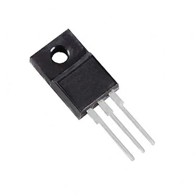
TO-220
•
•
•
•
•
•
High speed switching
Tight parameters distribution
Safe paralleling
Low thermal resistance
Short circuit rated
Ultrafast soft recovery antiparallel diode
Applications
•
•
•
Inverter
UPS
PFC
Description
This device is an IGBT developed using an advanced proprietary trench gate fieldstop structure. This IGBT series offers the optimum compromise between conduction
and switching losses, maximizing the efficiency of high frequency converters.
Furthermore, the positive VCE(sat) temperature coefficient and the tight parameter
distribution result in safer paralleling operation.
Product status link
STGP30H60DF
Product summary
Order code
STGP30H60DF
Marking
GP30H60DF
Package
TO-220
Packing
Tube
DS8709 - Rev 4 - September 2020
For further information contact your local STMicroelectronics sales office.
www.st.com
�STGP30H60DF
Electrical ratings
1
Electrical ratings
Table 1. Absolute maximum ratings
Symbol
Value
Unit
Collector-emitter voltage (VGE = 0 V)
600
V
Continuous collector current at TC = 25 °C
60
Continuous collector current at TC = 100 °C
30
ICP(1)
Pulsed collector current
120
A
VGE
Gate-emitter voltage
±20
V
Continuous forward current at TC = 25 °C
60
Continuous forward current at TC = 100 °C
30
IFP(1)
Pulsed forward current
120
A
PTOT
Total power dissipation at TC = 25 °C
260
W
Tstg
Storage temperature range
- 55 to 150
°C
Operating junction temperature range
- 55 to 175
°C
Value
Unit
VCES
IC
IF
TJ
Parameter
A
A
1. Pulse width limited by maximum junction temperature and turn-off within RBSOA.
Table 2. Thermal data
Symbol
RthJC
RthJA
DS8709 - Rev 4
Parameter
Thermal resistance junction-case IGBT
0.58
Thermal resistance junction-case diode
2.5
Thermal resistance junction-ambient
62.5
°C/W
°C/W
page 2/14
�STGP30H60DF
Electrical characteristics
2
Electrical characteristics
TC = 25 °C unless otherwise specified
Table 3. Static characteristics
Symbol
Parameter
Test conditions
V(BR)CES
Collector-emitter breakdown
voltage
VCE(sat)
Collector-emitter saturation
voltage
VGE(th)
Gate threshold voltage
VCE = VGE, IC = 1 mA
ICES
Collector cut-off current
IGES
Gate-emitter leakage current
VGE = 0 V, IC = 2 mA
Min.
Typ.
Max.
600
V
VGE = 15 V, IC = 30 A
2.0
VGE = 15 V, IC = 30 A, TJ = 175 °C
2.4
5
Unit
6
2.4
V
7
V
VGE = 0 V, VCE = 600 V
25
µA
VCE = 0 V, VGE = ±20 V
±250
nA
Table 4. Dynamic characteristics
Symbol
DS8709 - Rev 4
Parameter
Cies
Input capacitance
Coes
Output capacitance
Cres
Reverse transfer capacitance
Qg
Total gate charge
Qge
Gate-emitter charge
Qgc
Gate-collector charge
Test conditions
VCE = 25 V, f = 1 MHz, VGE = 0 V
VCC = 400 V, IC = 30 A, VGE = 0 to 15 V
(see Figure 20. Gate charge test circuit)
Min.
Typ.
Max.
Unit
-
3600
-
pF
-
130
-
pF
-
65
-
pF
-
105
-
nC
-
30
-
nC
-
35
-
nC
page 3/14
�STGP30H60DF
Electrical characteristics
Table 5. Switching characteristics (inductive load)
Symbol
td(on)
Parameter
Test conditions
Min.
Typ.
Max.
Unit
Turn-on delay time
VCE = 400 V, IC = 30 A,
50
-
ns
Current rise time
RG = 10 Ω, VGE = 15 V
15
-
ns
Turn-on current slope
(see Figure 19. Test circuit for inductive
load switching)
1600
-
A/µs
Turn-on delay time
VCE = 400 V, IC = 30 A,
47
-
ns
Current rise time
RG = 10 Ω, VGE = 15 V, TJ = 175 °C
17
-
ns
Turn-on current slope
(see Figure 19. Test circuit for inductive
load switching)
1400
-
A/μs
tr(Voff)
Off voltage rise time
VCE = 400 V, IC = 30 A,
20
-
ns
td(off)
Turn-off delay time
RG = 10 Ω, VGE = 15 V
160
-
ns
Current fall time
(see Figure 19. Test circuit for inductive
load switching)
60
-
ns
tr(Voff)
Off voltage rise time
VCE = 400 V, IC = 30 A,
22
-
ns
td(off)
Turn-off delay time
RG = 10 Ω, VGE = 15 V, TJ = 175 °C
146
-
ns
Current fall time
(see Figure 19. Test circuit for inductive
load switching)
88
-
ns
Short circuit withstand time
VCC ≤ 360 V, VGE = 15 V
3
6
-
µs
Min.
Typ.
Max.
Unit
tr
(di/dt)on
td(on)
tr
(di/dt)on
tf
tf
tsc
Table 6. Switching energy (inductive load)
Symbol
Parameter
Test conditions
Eon(1)
Turn-on switching losses
VCE = 400 V, IC = 30 A,
-
0.35
-
mJ
Eoff(2)
Turn-off switching losses
RG = 10 Ω, VGE = 15 V
-
0.40
-
mJ
Total switching losses
(see Figure 19. Test circuit for inductive
load switching)
-
0.75
-
mJ
Turn-on switching losses
VCE = 400 V, IC = 30 A,
-
0.84
-
mJ
Turn-off switching losses
RG = 10 Ω, VGE = 15 V, TJ = 175 °C
-
0.61
-
mJ
Total switching losses
(see Figure 19. Test circuit for inductive
load switching)
-
1.45
-
mJ
Ets
Eon(1)
(2)
Eoff
Ets
1. Energy losses include reverse recovery of the diode.
2. Turn-off losses include also the tail of the collector current.
DS8709 - Rev 4
page 4/14
�STGP30H60DF
Electrical characteristics
Table 7. Collector-emitter diode
Symbol
DS8709 - Rev 4
Parameter
VF
Forward on-voltage
trr
Reverse recovery time
Qrr
Reverse recovery charge
Irrm
Reverse recovery current
trr
Reverse recovery time
Qrr
Reverse recovery charge
Irrm
Reverse recovery current
Test conditions
Min.
Typ.
Max.
IF = 30 A
-
2.0
2.3
IF = 30 A, TJ = 175 °C
-
1.5
-
110
ns
-
136
nC
-
2.5
A
-
190
ns
-
506
nC
-
5.3
A
Vr = 400 V, IF = 30 A,
diF/dt = 100 A/μs
Vr = 400 V, IF = 30 A,
diF/dt = 100 A/μs, TJ = 175 °C
Unit
V
page 5/14
�STGP30H60DF
Electrical characteristics (curves)
2.1
Electrical characteristics (curves)
Figure 1. Output characteristics (TJ = 25 °C)
IC
(A)
11V
13V
80
AM17361v1
IC
(A)
AM17360v1
VGE=15V
100
Figure 2. Output characteristics (TJ = 175 °C)
VGE=15V
100
11V
80
13V
60
60
40
40
9V
9V
20
0
0
1
2
3
4
AM17362v1
100
TJ=-40°C
TJ=175°C
VCE=5V
7V
0
0
VCE(V)
Figure 3. Transfer characteristics
IC
(A)
20
1
2
4
3
VCE(V)
Figure 4. Normalized VGE(th) vs junction temperature
AM17369v1
VGE(th)
norm
1.0
TJ=25°C
80
0.9
60
0.8
40
0.7
20
0
7
8
9
10
11
VGE(V)
Figure 5. Power dissipation vs case temperature
AM17364v1
PTOT
(W)
240
0.6
-50
0
100
50
150 TJ(°C)
Figure 6. Collector current vs switching frequency
IC
(A)
60
200
50
160
120
40
80
30
40
rectangular current shape,
(duty cycle=0.5, Vcc= 400V Rg=10ohm,Vge=0/15V, Tj=175 °C)
0
0
DS8709 - Rev 4
25
50
75
100
125 150 TCASE(°C)
20
1
10
f(kHz)
page 6/14
�STGP30H60DF
Electrical characteristics (curves)
Figure 7. VCE(sat) vs junction temperature
AM17366v1
VCE(sat)
(V)
Figure 8. VCE(sat) vs collector current
AM17367v1
VCE(sat)
(V)
VGE=15V
VGE=15V
3.2
3.0
2.8
3.0
2.8
2.6
2.4
2.2
2.0
1.8
IC=60A
2.6
2.4
2.2
IC=30A
2.0
1.8
1.4
1.2
-50
TJ=25°C
1.6
1.4
IC=15A
1.6
TJ=175°C
0
50
100
150 TJ(°C)
TJ=-40°C
1.2
1.
10
20
Figure 9. Forward bias safe operating area
IC
(A)
AM17370v1
40
30
50
IC(A)
Figure 10. Thermal impedance
ZthTO2T_B
K
δ=0.5
lim
it
0.2
1µs
0.1
VC
E(s
at)
100
0.05
-1
10
0.02
10
100µs
Single pulse
(single pulse TC=25°C,
TJ15V
TJ