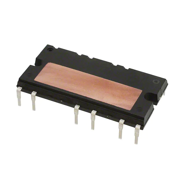
STGIPL35K120L1
SLLIMM™ (small low-loss intelligent molded module)
IPM, single phase - 35 A, 1200 V short-circuit rugged IGBT
Datasheet − preliminary data
Features
■
IPM 35 A, 1200 V single phase IGBT including
control ICs for gate driving and free-wheeling
diodes
■
Short-circuit rugged IGBTs
■
VCE(sat) negative temperature coefficient
■
Active Miller clamp feature
■
Undervoltage lockout
■
Desaturation detection
■
Fault status output
■
Input compatible with pulse transformer or
optocoupler
■
DBC substrate leading to low thermal
resistance
■
Isolation rating of 2500 Vrms/min
■
4.7 kΩ NTC for temperature control
)
s
(
ct
u
d
o
let
r
P
e
o
s
b
SDIP-18L
O
)
s
(
t
c
u
d
o
Applications
r
P
Description
e
t
e
l
o
s
b
O
■
Power inverters
This intelligent power module provides a compact,
high performance AC motor drive for a simple and
rugged design. It targets power inverters for air
conditioners. It combines ST proprietary control
ICs with the most advanced short-circuit rugged
IGBT system technology. SLLIMM™ is a
trademark of STMicroelectronics.
Table 1.
Device summary
Order code
Marking
Package
Packaging
STGIPL35K120L1
GIPL35K120L1
SDIP-18L
Tube
February 2013
Doc ID 022751 Rev 4
This is preliminary information on a new product now in development or undergoing evaluation. Details are subject to
change without notice.
1/19
www.st.com
19
�Contents
STGIPL35K120L1
Contents
1
Internal block diagram and pin configuration . . . . . . . . . . . . . . . . . . . . 3
2
Electrical ratings . . . . . . . . . . . . . . . . . . . . . . . . . . . . . . . . . . . . . . . . . . . . 5
3
2.1
Absolute maximum ratings . . . . . . . . . . . . . . . . . . . . . . . . . . . . . . . . . . . . . 5
2.2
Thermal data . . . . . . . . . . . . . . . . . . . . . . . . . . . . . . . . . . . . . . . . . . . . . . . 6
Electrical characteristics . . . . . . . . . . . . . . . . . . . . . . . . . . . . . . . . . . . . . 7
3.1
3.1.1
3.2
4
)
s
(
ct
Control part . . . . . . . . . . . . . . . . . . . . . . . . . . . . . . . . . . . . . . . . . . . . . . . . 9
u
d
o
NTC thermistor . . . . . . . . . . . . . . . . . . . . . . . . . . . . . . . . . . . . . . . . . . . 10
Recommendations . . . . . . . . . . . . . . . . . . . . . . . . . . . . . . . . . . . . . . . . . . 11
r
P
e
Functional description . . . . . . . . . . . . . . . . . . . . . . . . . . . . . . . . . . . . . . 12
t
e
l
o
4.1
Input . . . . . . . . . . . . . . . . . . . . . . . . . . . . . . . . . . . . . . . . . . . . . . . . . . . . . 12
4.2
Voltage reference . . . . . . . . . . . . . . . . . . . . . . . . . . . . . . . . . . . . . . . . . . . 12
4.3
Desaturation protection . . . . . . . . . . . . . . . . . . . . . . . . . . . . . . . . . . . . . . 12
4.4
Active Miller clamp . . . . . . . . . . . . . . . . . . . . . . . . . . . . . . . . . . . . . . . . . . 13
4.5
Fault status output . . . . . . . . . . . . . . . . . . . . . . . . . . . . . . . . . . . . . . . . . . 13
4.6
Undervoltage protection . . . . . . . . . . . . . . . . . . . . . . . . . . . . . . . . . . . . . . 13
)
(s
s
b
O
t
c
u
d
o
r
5
Package mechanical data . . . . . . . . . . . . . . . . . . . . . . . . . . . . . . . . . . . . 14
P
e
t
e
l
o
6
Revision history . . . . . . . . . . . . . . . . . . . . . . . . . . . . . . . . . . . . . . . . . . . 18
s
b
O
2/19
Doc ID 022751 Rev 4
�STGIPL35K120L1
1
Internal block diagram and pin configuration
Internal block diagram and pin configuration
Figure 1.
Internal block diagram
)
s
(
ct
u
d
o
r
P
e
t
e
l
o
)
(s
s
b
O
t
c
u
d
o
r
P
e
t
e
l
o
s
b
O
Doc ID 022751 Rev 4
3/19
�Internal block diagram and pin configuration
Table 2.
STGIPL35K120L1
Pin description
Pin
Symbol
1
VH-H
2
HIN
3
VREF-H
High side gate driver +5 V reference voltage
4
FAULT-H
High side gate driver fault output status
5
GND-H
High side gate driver ground
6
T1
NTC thermistor terminal 1
7
T2
NTC thermistor terminal 2
8
VH-L
9
LIN
10
VREF-L
Low side gate driver +5 V reference voltage
11
FAULT-L
Low side gate driver fault output status
12
GND-L
Low side gate driver ground
13
N
Negative DC input
14
N
Negative DC input
15
PHASE
Phase output
16
PHASE
Phase output
17
P
High side gate driver power supply
High side logic input (active low)
P
d
o
r
)
s
(
ct
Low side gate driver power supply
Low side logic input (active low)
u
d
o
r
P
e
t
e
l
o
)
(s
t
c
u
18
Figure 2.
Description
s
b
O
Positive DC input
Positive DC input
Pin layout (bottom view)
12 11 10 9
P
e
8
7
6
5
4
3
2
1
t
e
l
o
s
b
O
Marking area
13
14
15
16
17
18
AM09388v1
4/19
Doc ID 022751 Rev 4
�STGIPL35K120L1
Electrical ratings
2
Electrical ratings
2.1
Absolute maximum ratings
Table 3.
Inverter part
Symbol
Parameter
Value
Unit
1200
V
Each IGBT continuous collector current
at TC = 25°C
35
A
Each IGBT pulsed collector current
70
PTOT
Each IGBT total dissipation at TC = 25°C
100
tscw
Short circuit withstand time, VCE = 0.5 V(BR)CES
TJ = 125 °C, VH-H = 15 V, VI= 1 "logic state"
(s)
Each IGBT collector emitter voltage
VCE
± IC(1)
± ICP (2)
1. Calculated according to the iterative formula:
A
ct
du
5
W
µs
o
r
P
Tj ( max ) – TC
IC ( T C ) = ------------------------------------------------------------------------------------------------------R thj – c × V CE ( sat ) ( max ) ( T j ( max ), I C ( T C ) )
e
t
e
ol
2. Pulse width limited by max junction temperature
Table 4.
Control part
Symbol
VH
)
(s
ct
Vfault
Voltage on FAULT pin
Vother
Voltage on other pins (IN, VREF)
ete
du
o
r
P
Symbol
s
b
O
Parameter
Maximum VH-H, VH-L voltages vs. GND
Table 5.
ol
s
b
O
Value
Unit
28
V
-0.3 to VH+0.3
V
-0.3 to 7
V
Value
Unit
2500
V
Total system
Parameter
VISO
Isolation withstand voltage applied between each
pin and heatsink plate (AC voltage, t = 60 sec.)
TJ (1)
Operating junction temperature for IGBT and diode
-40 to 150
°C
Module case operation temperature
-40 to 125
°C
TC
1. The maximum junction temperature rating of the power chips integrated within the SDIP module is 150 °C
(@TC ≤ 100 °C). To ensure safe operation of the NDIP module, the average junction temperature should
be limited to TJ(avg) ≤ 125 °C (@TC ≤ 100 °C).
Doc ID 022751 Rev 4
5/19
�Electrical ratings
2.2
STGIPL35K120L1
Thermal data
Table 6.
Thermal data
Symbol
RthJC
Figure 3.
Parameter
Value
Unit
Thermal resistance junction-case single IGBT
0.9
°C/W
Thermal resistance junction-case single diode
1.4
°C/W
Transient thermal impedance IGBT/diode - inverter
AM09392v1
10
)
s
(
ct
DIODE
ZTH(J-C) [K/W]
1
0.1
t
e
l
o
0.01
1.E-05
1.E-04
od
r
P
e
)
(s
t
c
u
0.001
1.E-03
s
b
O
1.E-02
time [s]
t
e
l
o
s
b
O
6/19
u
d
o
r
P
e
IGBT
Doc ID 022751 Rev 4
1.E-01
1.E+00
1.E+01
�STGIPL35K120L1
3
Electrical characteristics
Electrical characteristics
TJ = 25 °C unless otherwise specified.
Table 7.
Inverter part
Value
Symbol
Parameter
ICES
VF
Unit
Min.
Typ.
Max.
VH-H (VH-L) = 15 V, VIN (1) = 1 "logic
state", IC = 30 A
-
2.8
3.6
VH-H (VH-L) = 15 V, VIN (1) = 1 "logic
state", IC = 30 A, TJ = 125°C
-
2.4
Collector-cut off current
(VIN (1)= 0 “logic state”)
VCE = 1200 V, VH-H (VH-L) = 15 V
-
Diode forward voltage
VIN (1) = 0 "logic state", IF = 30 A
-
u
d
o
-
720
-
-
300
-
-
880
-
-
275
-
-
520
-
-
3.7
-
-
1.9
-
-
820
-
-
350
-
-
1400
-
-
700
-
-
620
-
-
5.6
-
-
5.8
-
Collector-emitter
saturation voltage
VCE(sat)
Test conditions
V
r
P
e
Switching on/off (inductive load) (2)
ton
tc(on)
Crossover time (on)
toff
Turn-off time
tc(off)
Crossover time (off)
trr
Reverse recovery time
Eon
Turn-on switching losses
Eoff
Turn-off switching losses
ton
Turn-on time
toff
e
t
e
l
tc(off)
o
s
b
O
Pr
Turn-off time
o
s
b
VDD = 600 V,
VH-H (VH-L) = 15 V,
VIN = 1 "logic state" (see Table 9)
IC = 30 A (see Figure 4 and 5)
O
)
s
(
t
c
u
d
o
Crossover time (on)
tc(on)
trr
let
Turn-on time
Crossover time (off)
Reverse recovery time
Eon
Turn-on switching losses
Eoff
Turn-off switching losses
VDD = 600 V,
VH-H (VH-L) = 15 V,
VIN = 1 "logic state" (see Table 9)
IC = 30 A, TJ = 125 °C
(see Figure 4 and 5)
)
s
(
ct
10
mA
2.3
V
ns
mJ
ns
mJ
1. See Table 9: Truth table.
2. tON and tOFF include the propagation delay time of the internal drive. tC(ON) and tC(OFF) are the switching time of IGBT itself
under the internally given gate driving condition. Parameter values take into account a 20 nH stray inductance.
Doc ID 022751 Rev 4
7/19
�Electrical characteristics
Figure 4.
STGIPL35K120L1
Switching time test circuit
)
s
(
ct
u
d
o
r
P
e
t
e
l
o
Figure 5.
s
b
O
Switching time definition
)
(s
100% IC 100% IC
t rr
t
c
u
od
r
P
e
IC
VCE
VCE
IC
t
e
l
o
s
b
O
VIN
VIN
t ON
t OFF
t C(OFF)
t C(ON)
VIN(ON)
10% IC 90% IC 10% VCE
(a) turn-on
8/19
VIN(OFF)
10% VCE
(b) turn-off
Doc ID 022751 Rev 4
10% IC
AM09390v1
�STGIPL35K120L1
3.1
Electrical characteristics
Control part
TA = - 20 to 125 °C, VH = 16 V (unless otherwise specified).
Table 8.
Electrical characteristics
Symbol
Parameter
Test condition
Min
Typ
0.8
1.0
Max
Unit
Input
Vton
IN turn-on threshold voltage
Vtoff
IN turn-off threshold voltage
tonmin
Iinp
Minimum pulse width
100
V
4.0
4.2
V
135
220
ns
1
µA
(s)
IN input current
t
c
u
Voltage reference (1)
Vref
Voltage reference
Iref
Maximum output current
Tmin < T < Tmax
4.77
Fault output
tfault
Delay for fault detection
VFL
FAULT low voltage
UVLO top threshold
UVLOL
UVLO bottom threshold
Vhyst
)
(s
ct
UVLO hysteresis
u
d
o
Supply current
Quiescent current
Iin
e
t
e
l
so
IFLsink = 10 mA
Under voltage lockout (UVLO)
UVLOH
Pr
10
5.22
od
b
O
UVLOH-UVLOL
mA
500
ns
1
V
10
11
12
V
9
10
11
V
0.5
1
V
Output = 0 V, no load
r
P
e
V
5
mA
1. Recommended capacitor range on VREF pin is 10 nF to 100 nF.
t
e
l
o
Table 9.
bs
Truth table
Logic input (VI)
Output
Condition
LIN
HIN
Low side gate
driver output
High side gate
driver output
0 ‘’logic state”
half-bridge tri-state
H
H
L
L
1 “logic state”
low side direct driving
L
H
H
L
1 “logic state”
high side direct driving
H
L
L
H
O
Note:
X: don’t care
Doc ID 022751 Rev 4
9/19
�Electrical characteristics
3.1.1
STGIPL35K120L1
NTC thermistor
Table 10.
NTC thermistor
Symbol
Parameter
Test conditions
Min.
Typ. Max. Unit.
R25
Resistance
TC = 25°C
4.7
kΩ
R125
Resistance
TC = 125°C
160
Ω
B
B-constant
TC = 25°C
3950
K
T
Operating temperature
-40
Equation 1: resistance variation vs. temperature
150
R ( T ) = R 25 ⋅ e
Figure 6.
NTC resistance vs. temperature
100
)
(s
od
let
o
s
b
O
10/19
r
P
e
AM07843v1
s
b
O
t
c
u
10
r
P
e
u
d
o
t
e
l
o
R (kΩ)
)
s
(
ct
1
1
B ⎛ --- – ----------⎞
⎝ T 298⎠
Where T are temperatures in Kelvins
1
0.1
0.01
-50
0
50
Doc ID 022751 Rev 4
100
°C
T (°C)
�STGIPL35K120L1
3.2
Electrical characteristics
Recommendations
●
As the IPM may be used in a very noisy environment, care should be taken to decouple
the supplies. Small ceramic capacitors, connected inside the IPM as close as possible
to the gate driver pins, are used to improve noise-withstand capability.
●
The IPM is compatible with both pulse transformers or optocouplers. When using an
optocoupler, the IN input must be limited to approximately 5 V. The pull-up resistor to
VH must be between 5 kΩ and 20 kΩ, depending on optocoupler characteristics. An
optional filtering capacitor can be added in the event of a highly noisy environment,
although the IPM already includes a filtering on input signals and rejects signals
smaller than 100 ns (tONMIN specification).
●
When using a pulse transformer, a 2.5 V reference point can be built from the 5 V VREF
pin with a resistor divider. The capacitor between the VREF pin and the resistor divider
middle point provides decoupling of the 2.5 V reference, and also ensures a high level
on the IN input pin at power-up to start the IPM in OFF state. The waveform from the
pulse transformer must comply with the tONMIN and VtON / VtOFF specifications. To turn
ON the IPM outputs, the input signal must be lower than 0.8 V for at least 220 ns.
Conversely, the input signal must be higher than 4.2 V for at least 200 ns to turn OFF
the outputs. A pulse width of about 500 ns at these threshold levels is recommended. In
all cases, the input signal at the IN pin must be between 0 and 5 V.
)
s
(
ct
u
d
o
r
P
e
t
e
l
o
●
To prevent the input signals oscillation, the wiring of each input should be as short as
possible.
●
Electrolytic bus capacitors should be mounted as close to the module bus terminals as
possible. Additional high frequency ceramic capacitor mounted close to the module
pins will further improve performance.
●
When setting the maximum voltage to be applied between P-N, the internal stray
inductance and the maximum di/dt should be considered. Due to both internal and
layout stray inductances, the di/dt results in a voltage surges between the DC-link
capacitor and the switches during commutations.
)
(s
s
b
O
●
t
c
u
d
o
r
FAULT pin is externally available to provide a feedback signal about IPM status. Please
refer to undervoltage protection and desaturation fault timing diagrams for more
information. Fault output signals the undervoltage state and is reset only when
undervoltage state disappears. When a desaturation event occurs, the fault output is
pulled down and IPM outputs are low (IGBT off) until the IN input signal is released
(high level), then activated again (low level).
P
e
t
e
l
o
s
b
O
Doc ID 022751 Rev 4
11/19
�Functional description
STGIPL35K120L1
4
Functional description
4.1
Input
The input is compatible with optocouplers or pulse transformers. The input is triggered by
the signal edge and allows the use of low-sized, low-cost pulse transformer. Input is active
low (output is high when input is low) to ease the use of optocoupler. When driven by a pulse
transformer, the input pulse (positive and negative) width must be larger than the minimum
pulse width tonmin.
4.2
Voltage reference
)
s
(
ct
A voltage reference is used to create accurate timing for the two-level turn-off with external
resistor and capacitor.
4.3
u
d
o
r
P
e
Desaturation protection
t
e
l
o
The desaturation function provides a protection against over-current events. Voltage across
the IGBT is monitored, and the IGBT is turned off if the voltage threshold is reached. A
blanking time is made of an internal current source and a capacitor.
s
b
O
During operation, the DESAT capacitor is discharged when IPM output is low (IGBT off).
When the IGBT is turned on, the DESAT capacitor starts charging and desaturation
protection is effective after the blanking time (fixed by design showing a typical value of 2
µs).
)
(s
t
c
u
When a desaturation event occurs, the fault output is pulled down and IPM outputs are low
(IGBT off) until the IN input signal is released (high level), then activated again (low level).
d
o
r
Figure 7.
Desaturation 1200 V
P
e
t
e
l
o
s
b
O
12/19
Doc ID 022751 Rev 4
�STGIPL35K120L1
4.4
Functional description
Active Miller clamp
A Miller clamp allows the control of the Miller current during a high dV/dt situation and can
avoid the use of a negative supply voltage.
During turn-off, the gate voltage is monitored and the clamp output is activated when gate
voltage goes below 2 V (relative to GND). The clamp is disabled when the IN input is
triggered again.
4.5
Fault status output
Fault output is used to signal a fault event (desaturation, UVLO) to a controller. The fault pin
is designed to drive an optocoupler.
4.6
)
s
(
ct
Undervoltage protection
u
d
o
Undervoltage detection protects the application in the event of a low VH supply voltage
(during start-up or a fault situation). Fault output signals the undervoltage state and is reset
only when undervoltage state disappears.
Figure 8.
r
P
e
t
e
l
o
Undervoltage protection
bs
O
)
VH
OUT
s
(
t
c
UVH
UVL
VH-Hmin
2V
u
d
o
r
P
e
FAULT
AM17097v1
t
e
l
o
s
b
O
Doc ID 022751 Rev 4
13/19
�Package mechanical data
5
STGIPL35K120L1
Package mechanical data
In order to meet environmental requirements, ST offers these devices in different grades of
ECOPACK® packages, depending on their level of environmental compliance. ECOPACK®
specifications, grade definitions and product status are available at: www.st.com.
ECOPACK® is an ST trademark.
Please refer to dedicated technical note TN0107 for mounting instructions.
Table 11.
SDIP-18L package mechanical data
mm.
)
s
(
ct
Dim.
Min.
Typ.
A
49.10
49.60
A1
1.10
1.30
A2
1.40
1.60
A3
44.10
44.60
B
24.00
B1
11.25
B2
27.10
C
5.00
1.80
45.10
25.00
27.60
28.10
5.40
6.00
6.50
7.00
7.50
10.35
10.85
11.35
2.40
2.60
2.80
11.80
12.00
12.20
e2
7.10
7.30
7.50
e3
4.50
4.70
4.90
e4
5.80
6.00
6.20
e5
6.30
6.50
6.70
e6
10.40
10.60
10.80
e7
17.00
17.20
17.40
e
)
s
(
ct
u
d
o
e1
14/19
1.50
12.45
C2
s
b
O
o
s
b
Pr
u
d
o
50.10
11.85
C1
e
t
e
ol
e
t
e
l
24.50
Max.
Pr
-O
D
38.00
D1
5.70
E
11.80
E1
2.15
F
0.85
1.00
1.15
F1
0.35
0.50
0.65
R
1.55
1.75
1.95
T
0.45
0.55
0.65
V
0°
Doc ID 022751 Rev 4
6°
�STGIPL35K120L1
Figure 9.
Package mechanical data
SDIP-18L package drawing (dimensions are in mm.)
)
s
(
ct
u
d
o
r
P
e
t
e
l
o
)
(s
s
b
O
t
c
u
d
o
r
P
e
t
e
l
o
8243339_D
s
b
O
Doc ID 022751 Rev 4
15/19
�Package mechanical data
STGIPL35K120L1
Figure 10. SDIP-18L shipping tube type A (dimensions are in mm.)
)
s
(
ct
r
P
e
t
e
l
o
)
(s
s
b
O
t
c
u
d
o
r
P
e
t
e
l
o
s
b
O
16/19
Doc ID 022751 Rev 4
8147106_E
u
d
o
�STGIPL35K120L1
Package mechanical data
Figure 11. SDIP-18L shipping tube type B (dimensions are in mm.)
)
s
(
ct
u
d
o
t
e
l
o
)
(s
s
b
O
8147106_E
r
P
e
t
c
u
d
o
r
P
e
t
e
l
o
s
b
O
Doc ID 022751 Rev 4
17/19
�Revision history
6
STGIPL35K120L1
Revision history
Table 12.
Document revision history
Date
Revision
Changes
30-Jan-2012
1
Initial release.
28-Feb-2012
2
Added: VCE(sat) max. value Table 7 on page 7.
15-Oct-2012
3
Modified: VF max. value 2.3 V Table 7 on page 7.
07-Feb-2013
4
Modified: tscw parameter Table 3 on page 5.
Updated: Figure 8 on page 13.
u
d
o
)
s
(
ct
r
P
e
t
e
l
o
)
(s
s
b
O
t
c
u
d
o
r
P
e
t
e
l
o
s
b
O
18/19
Doc ID 022751 Rev 4
�STGIPL35K120L1
)
s
(
ct
Please Read Carefully:
u
d
o
Information in this document is provided solely in connection with ST products. STMicroelectronics NV and its subsidiaries (“ST”) reserve the
right to make changes, corrections, modifications or improvements, to this document, and the products and services described herein at any
time, without notice.
r
P
e
All ST products are sold pursuant to ST’s terms and conditions of sale.
Purchasers are solely responsible for the choice, selection and use of the ST products and services described herein, and ST assumes no
liability whatsoever relating to the choice, selection or use of the ST products and services described herein.
t
e
l
o
No license, express or implied, by estoppel or otherwise, to any intellectual property rights is granted under this document. If any part of this
document refers to any third party products or services it shall not be deemed a license grant by ST for the use of such third party products
or services, or any intellectual property contained therein or considered as a warranty covering the use in any manner whatsoever of such
third party products or services or any intellectual property contained therein.
)
(s
s
b
O
UNLESS OTHERWISE SET FORTH IN ST’S TERMS AND CONDITIONS OF SALE ST DISCLAIMS ANY EXPRESS OR IMPLIED
WARRANTY WITH RESPECT TO THE USE AND/OR SALE OF ST PRODUCTS INCLUDING WITHOUT LIMITATION IMPLIED
WARRANTIES OF MERCHANTABILITY, FITNESS FOR A PARTICULAR PURPOSE (AND THEIR EQUIVALENTS UNDER THE LAWS
OF ANY JURISDICTION), OR INFRINGEMENT OF ANY PATENT, COPYRIGHT OR OTHER INTELLECTUAL PROPERTY RIGHT.
t
c
u
d
o
r
UNLESS EXPRESSLY APPROVED IN WRITING BY TWO AUTHORIZED ST REPRESENTATIVES, ST PRODUCTS ARE NOT
RECOMMENDED, AUTHORIZED OR WARRANTED FOR USE IN MILITARY, AIR CRAFT, SPACE, LIFE SAVING, OR LIFE SUSTAINING
APPLICATIONS, NOR IN PRODUCTS OR SYSTEMS WHERE FAILURE OR MALFUNCTION MAY RESULT IN PERSONAL INJURY,
DEATH, OR SEVERE PROPERTY OR ENVIRONMENTAL DAMAGE. ST PRODUCTS WHICH ARE NOT SPECIFIED AS "AUTOMOTIVE
GRADE" MAY ONLY BE USED IN AUTOMOTIVE APPLICATIONS AT USER’S OWN RISK.
P
e
t
e
l
o
Resale of ST products with provisions different from the statements and/or technical features set forth in this document shall immediately void
any warranty granted by ST for the ST product or service described herein and shall not create or extend in any manner whatsoever, any
liability of ST.
s
b
O
ST and the ST logo are trademarks or registered trademarks of ST in various countries.
Information in this document supersedes and replaces all information previously supplied.
The ST logo is a registered trademark of STMicroelectronics. All other names are the property of their respective owners.
© 2013 STMicroelectronics - All rights reserved
STMicroelectronics group of companies
Australia - Belgium - Brazil - Canada - China - Czech Republic - Finland - France - Germany - Hong Kong - India - Israel - Italy - Japan Malaysia - Malta - Morocco - Philippines - Singapore - Spain - Sweden - Switzerland - United Kingdom - United States of America
www.st.com
Doc ID 022751 Rev 4
19/19
�


 工商网监
湘ICP备2023018690号
工商网监
湘ICP备2023018690号
