STGW20NB60KD
N-CHANNEL 20A - 600V TO-247
SHORT CIRCUIT PROOF PowerMESH™ IGBT
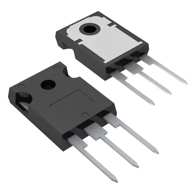
Figure 1: Package
Table 1: General Features
TYPE
VCES
VCE(sat) (Max)
@25°C
IC
@100°C
STGW20NB60KD
600 V
< 2.8 V
25 A
■
■
■
■
■
■
■
■
■
OFF LOSSES INCLUDE TAIL CURRENT
HIGH CURRENT CAPABILITY
HIGH INPUT IMPEDANCE (VOLTAGE
DRIVEN)
LOW ON-VOLTAGE DROP (Vcesat)
LOW ON-LOSSES
LOW GATE CHARGE
VERY HIGH FREQUENCY OPERATION
SHORT CIRCUIT RATED
LATCH CURRENT FREE OPERATION
3
2
1
c
u
d
TO-247
o
r
P
Weight: 4.41gr ± 0.01
Max Clip Pressure: 150 N/mm2
DESCRIPTION
Using the latest high voltage technology based on
a patented strip layout, STMicroelectronics has
designed an advanced family of IGBTs, the PowerMESH™ IGBTs, with outstanding performances.
The suffix “K” identifies a family optimized for high
frequency motor control applications with short circuit withstand capability.
)
s
(
ct
)
s
t(
e
t
le
Figure 2: Internal Schematic Diagram
o
s
b
O
-
APPLICATIONS
HIGH FREQUENCY MOTOR CONTROLS
■ U.P.S
■ WELDING EQUIPMENTS
u
d
o
■
r
P
e
t
e
l
o
Table 2: Order Codes
s
b
O
SALES TYPE
MARKING
PACKAGE
PACKAGING
STGW20NB60KD
GW20NB60KD
TO-247
TUBE
Rev. 3
May 2005
1/11
�STGW20NB60KD
Table 3: Absolute Maximum ratings
Symbol
Parameter
Value
Unit
VCES
Collector-Emitter Voltage (VGS = 0)
600
V
VECR
Reverse Battery Protection
20
V
VGE
Gate-Emitter Voltage
± 20
V
IC
Collector Current (continuous) at 25°C (#)
50
A
IC
Collector Current (continuous) at 100°C (#)
25
A
Collector Current (pulsed)
100
A
ICM (1)
TSC
Short Circuit Withstand
10
µs
PTOT
Total Dissipation at TC = 25°C
170
W
Derating Factor
1.2
W/°C
– 55 to 150
°C
Tstg
Tj
Storage Temperature
Operating Junction Temperature
(1)Pulse width limited by max. junction temperature.
Table 4: Thermal Data
Min.
Typ.
Rthj-case
Thermal Resistance Junction-case
--
--
Rthj-amb
Thermal Resistance Junction-ambient
--
P
e
let
Electrical Characteristics (Tcase =25°C unless otherwise specified)
Table 5: Off
so
Symbol
Parameter
VBR(CES)
Collectro-Emitter Breakdown
Voltage
IC = 250 µA, VGE = 0
Collector-Emitter Leakage
Current (VCE = 0)
VGE = Max Rating
Tc=25°C
Tc=125°C
Gate-Emitter Leakage
Current (VCE = 0)
VGE = ± 20 V , VCE = 0
ICES
IGES
)
s
(
ct
u
d
o
Table 6: On
r
P
e
Symbol
VGE(th)
Test Conditions
Parameter
s
b
O
Test Conditions
VCE= VGE, IC= 250 µA
Collector-Emitter Saturation
Voltage
VGE= 15 V, IC= 20A, Tj= 25°C
VGE= 15 V, IC= 20A,
Tj= 125°C
(#) Calculated according to the iterative formula:
T
–T
JMAX
C
I ( T ) = -------------------------------------------------------------------------------------------------C C
R
×V
(T , I )
THJ – C
CESAT ( M AX ) C C
2/11
b
O
-
Gate Threshold Voltage
t
e
l
o
VCE(SAT)
d
o
r
Min.
uc
--
Typ.
)
s
t(
Max.
0.73
°C/W
50
°C/W
Max.
Unit
600
Min.
V
10
100
µA
µA
± 100
nA
Typ.
Max.
Unit
7
V
2.3
1.9
2.8
V
V
5
�STGW20NB60KD
ELECTRICAL CHARACTERISTICS (CONTINUED)
Table 7: Dynamic
Symbol
Parameter
Test Conditions
Forward Transconductance
VCE = 25 V, IC= 20 A
Cies
Coes
Cres
Input Capacitance
Output Capacitance
Reverse Transfer
Capacitance
Qg
Qge
Qgc
tscw
gfs
Min.
Typ.
Max.
Unit
8
S
VCE = 25V, f = 1 MHz, VGE = 0
1560
190
38
pF
pF
pF
Total Gate Charge
Gate-Emitter Charge
Gate-Collector Charge
VCE = 480 V, IC = 20 A,
VGE = 15V,
(see Figure 19)
85
14.4
51
Short Circuit Withstand Time
Vce = 0.5 BVces , Tj = 125°C
RG = 10 Ω, VGE= 15V
115
10
nC
nC
nC
µs
Table 8: Switching On
Symbol
td(on)
tr
(di/dt)on
Eon (2)
Parameter
Test Conditions
Min.
Typ.
Turn-on Delay Time
Current Rise Time
VCC = 480 V, IC = 20 A
RG= 10Ω, VGE= 15V, Tj= 25°C
(see Figure 17)
39
35
Turn-on Current Slope
Turn-on Switching Losses
VCC = 480 V, IC = 20 A
RG= 10Ω, VGE= 15V, Tj= 125°C
(see Figure 17)
453
675
)
s
t(
Max.
c
u
d
o
r
P
Unit
ns
ns
A/µs
µJ
2) Eon is the turn-on losses when a typical diode is used in the test circuit in Figure 17. If the IGBT is offered in a package with a co-pack
diode, the co-pack diode is used as external diode.
Table 9: Switching Off
Symbol
tr(Voff)
tc
td(off)
tf
Eoff (3)
Ets
tr(Voff)
tc
Parameter
Cross-over Time
tf
s
b
O
Eoff (3)
Ets
ct
Current Fall Time
Turn-off Switching Loss
u
d
o
r
P
e
Off Voltage Rise Time
Cross-over Time
t
e
l
o
td(off)
(s)
Turn-off Delay Time
Total Switching Loss
Turn-off Delay Time
o
s
b
O
Test Conditions
Vcc = 480 V, IC = 20 A,
RGE = 10 Ω , VGE = 15 V
TJ = 25 °C
(see Figure 17)
Off Voltage Rise Time
e
t
le
Vcc = 480 V, IC = 20 A,
RGE = 10 Ω , VGE = 15 V
Tj = 125 °C
(see Figure 17)
Min.
Typ.
Max.
Unit
25
ns
160
ns
105
ns
95
ns
0.5
mJ
0.9
mJ
46
ns
175
ns
130
ns
Current Fall Time
150
ns
Turn-off Switching Loss
0.70
mJ
Total Switching Loss
1.35
mJ
(3)Turn-off losses include also the tail of the collector current.
3/11
�STGW20NB60KD
Table 10: Collector-Emitter Diode
Symbol
Parameter
Test Conditions
Min.
Typ.
If
Ifm
Forward Current
Forward Current pulsed
Vf
Forward On-Voltage
If = 10 A
If = 10 A, Tj = 125 °C
1.27
1
Reverse Recovery Time
Reverse Recovery Charge
Reverse Recovery Current
If = 10 A ,VR = 27 V,
Tj =125°C, di/dt = 100 A/μs
(see Figure 20)
80.5
181
4.5
trr
Qrr
Irrm
Max.
Unit
20
80
A
A
2.0
V
V
c
u
d
e
t
le
)
s
(
ct
u
d
o
r
P
e
t
e
l
o
s
b
O
4/11
o
s
b
O
-
o
r
P
ns
nC
A
)
s
t(
�STGW20NB60KD
Figure 3: Output Characteristics
Figure 6: Transfer Characteristics
Figure 4: Transconductance
Figure 7: Collector-Emitter On Voltage vs Temperature
c
u
d
e
t
le
)
s
(
ct
o
r
P
o
s
b
O
-
Figure 5: Collector-Emitter On Voltage vs Collector Current
u
d
o
)
s
t(
Figure 8: Normalized Gate Threshold vs Temperature
r
P
e
t
e
l
o
s
b
O
5/11
�STGW20NB60KD
Figure 9: Normalized Breakdown Voltage vs
Temperature
Figure 12: Gate Charge vs Gate-Emitter Voltage
Figure 10: Capacitance Variations
Figure 13: Diode Forward Voltage
c
u
d
e
t
le
)
s
(
ct
r
P
e
t
e
l
o
s
b
O
6/11
o
r
P
o
s
b
O
-
Figure 11: Turn-Off Energy Losses vs Temperature
u
d
o
)
s
t(
Figure 14: Total Switching Losses vs Collector
Current
�STGW20NB60KD
Figure 15: Thermal Impedance
Figure 16: Turn-Off SOA
c
u
d
e
t
le
)
s
(
ct
)
s
t(
o
r
P
o
s
b
O
-
u
d
o
r
P
e
t
e
l
o
s
b
O
7/11
�STGW20NB60KD
Figure 17: Test Circuit for Inductive Load
Switching
Figure 19: Gate Charge Test Circuit
Figure 18: Switching Waveforms
Figure 20: Diode Recovery Times Waveform
c
u
d
e
t
le
)
s
(
ct
u
d
o
r
P
e
t
e
l
o
s
b
O
8/11
o
s
b
O
-
o
r
P
)
s
t(
�STGW20NB60KD
TO-247 MECHANICAL DATA
mm.
DIM.
MIN.
TYP
inch
MAX.
MIN.
TYP.
MAX.
A
4.85
5.15
0.19
0.20
A1
2.20
2.60
0.086
0.102
b
1.0
1.40
0.039
0.055
b1
2.0
2.40
0.079
0.094
0.134
b2
3.0
3.40
0.118
c
0.40
0.80
0.015
0.03
D
19.85
20.15
0.781
0.793
E
15.45
15.75
0.608
e
5.45
L
14.20
L1
3.70
L2
14.80
0.560
4.30
0.14
18.50
øP
3.55
3.65
0.140
4.50
5.50
0.177
)
s
(
ct
uc
0.17
r
P
e
t
le
5.50
)
s
t(
0.582
0.728
øR
S
0.620
0.214
od
0.143
0.216
0.216
o
s
b
O
-
u
d
o
r
P
e
t
e
l
o
s
b
O
9/11
�STGW20NB60KD
Table 11:
Revision History
Date
Revision
21-Mar-2005
05-Apr-2005
2
3
Description of Changes
New stylesheet. Some value changed on Table 3 and 4
New updated values in table 3
c
u
d
e
t
le
)
s
(
ct
u
d
o
r
P
e
t
e
l
o
s
b
O
10/11
o
s
b
O
-
o
r
P
)
s
t(
�STGW20NB60KD
c
u
d
e
t
le
)
s
(
ct
)
s
t(
o
r
P
o
s
b
O
-
u
d
o
r
P
e
Information furnished is believed to be accurate and reliable. However, STMicroelectronics assumes no responsibility for the consequences
of use of such information nor for any infringement of patents or other rights of third parties which may result from its use. No license is granted
by implication or otherwise under any patent or patent rights of STMicroelectronics. Specifications mentioned in this publication are subject
to change without notice. This publication supersedes and replaces all information previously supplied. STMicroelectronics products are not
authorized for use as critical components in life support devices or systems without express written approval of STMicroelectronics.
t
e
l
o
s
b
O
The ST logo is a registered trademark of STMicroelectronics
All other names are the property of their respective owners
© 2005 STMicroelectronics - All Rights Reserved
STMicroelectronics group of companies
Australia - Belgium - Brazil - Canada - China - Czech Republic - Finland - France - Germany - Hong Kong - India - Israel - Italy - Japan Malaysia - Malta - Morocco - Singapore - Spain - Sweden - Switzerland - United Kingdom - United States of America
www.st.com
11/11
�
很抱歉,暂时无法提供与“STGW20NB60KD”相匹配的价格&库存,您可以联系我们找货
免费人工找货