STGFW30H65FB, STGW30H65FB
Datasheet
Trench gate field-stop 650 V, 30 A high speed HB series IGBT
Features
1
1
2
3
1
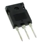
TO-247
TO-3PF
2
•
Maximum junction temperature: TJ = 175 °C
•
•
•
High speed switching series
Minimized tail current
VCE(sat) = 1.55 V (typ.) at IC = 30 A
•
•
•
Tight parameters distribution
Safe paralleling
Low thermal resistance
3
Applications
C(2, TAB)
•
•
•
•
G(1)
Photovoltaic inverters
Power factor correction
Welding
High-frequency converters
Description
E(3)
G1C2TE3
These devices are IGBTs developed using an advanced proprietary trench gate
field-stop structure. These devices are part of the new HB series of IGBTs, which
represent an optimum compromise between conduction and switching loss to
maximize the efficiency of any frequency converter. Furthermore, the slightly positive
VCE(sat) temperature coefficient and very tight parameter distribution result in safer
paralleling operation.
Product status links
STGFW30H65FB
STGW30H65FB
DS10155 - Rev 7 - March 2021
For further information contact your local STMicroelectronics sales office.
www.st.com
�STGFW30H65FB, STGW30H65FB
Electrical ratings
1
Electrical ratings
Table 1. Absolute maximum ratings
Symbol
VCES
Value
Parameter
TO-247
TO-3PF
Unit
Collector-emitter voltage (VGE = 0 V)
650
V
Continuous collector current at TC = 25 °C
60
A
Continuous collector current at TC = 100 °C
30
A
ICP
Pulsed collector current
120
A
VGE
Gate-emitter voltage
±20
V
PTOT
Total power dissipation at TC = 25 °C
VISO
Insulation withstand voltage (RMS) from all three leads to external
heat sink (t = 1 s; Tc = 25 °C)
Tstg
Storage temperature range
-55 to 150
°C
Operating junction temperature range
-55 to 175
°C
IC
(1)
TJ
260
92
W
3.5
kV
1. Pulse width is limited by maximum junction temperature.
Table 2. Thermal data
Symbol
DS10155 - Rev 7
Parameter
RthJC
Thermal resistance, junction-to-case
RthJA
Thermal resistance, junction-to-ambient
Value
TO-247
TO-3PF
0.58
1.63
50
Unit
°C/W
°C/W
page 2/18
�STGFW30H65FB, STGW30H65FB
Electrical characteristics
2
Electrical characteristics
TJ = 25 °C unless otherwise specified
Table 3. Static characteristics
Symbol
Parameter
Test conditions
V(BR)CES
Collector-emitter breakdown
voltage
VCE(sat)
Collector-emitter saturation
voltage
VGE = 0 V, IC = 2 mA
Min.
Typ.
650
1.55
VGE = 15 V, IC = 30 A, TJ = 125 °C
1.65
VGE = 15 V, IC = 30 A, TJ = 175 °C
1.75
Gate threshold voltage
VCE = VGE, IC = 1 mA
ICES
Collector cut-off current
IGES
Gate-emitter leakage current
5
Unit
V
VGE = 15 V, IC = 30 A
VGE(th)
Max.
6
2
V
7
V
VGE = 0 V, VCE = 650 V
25
µA
VCE = 0 V, VGE = ±20 V
250
nA
Table 4. Dynamic characteristics
Symbol
Cies
Input capacitance
Coes
Output capacitance
Cres
Reverse transfer capacitance
Qg
DS10155 - Rev 7
Parameter
Test conditions
VCE = 25 V, f = 1 MHz, VGE = 0 V
Total gate charge
Qge
Gate-emitter charge
Qgc
Gate-collector charge
VCC = 520 V, IC = 30 A, VGE = 0 to 15 V
(see Figure 27. Gate charge test circuit)
Min.
Typ.
Max.
Unit
-
3659
-
pF
-
101
-
pF
-
76
-
pF
-
149
-
nC
-
25
-
nC
-
62
-
nC
page 3/18
�STGFW30H65FB, STGW30H65FB
Electrical characteristics
Table 5. Switching characteristics (inductive load)
Symbol
td(on)
tr
(di/dt)on
td(off)
tf
Parameter
Min.
Typ.
Max.
Unit
Turn-on delay time
-
37
-
ns
Current rise time
-
14.6
-
ns
-
1643
-
A/µs
-
146
-
ns
-
23
-
ns
-
151
-
µJ
Turn-on current slope
Turn-off delay time
Current fall time
Test conditions
VCE = 400 V, IC = 30 A,
RG = 10 Ω, VGE = 15 V
(see Figure 26. Test circuit for inductive
load switching)
(1)
Turn-on switching energy
Eoff (2)
Turn-off switching energy
-
293
-
µJ
Total switching energy
-
444
-
µJ
Turn-on delay time
-
35
-
ns
Current rise time
-
16.1
-
ns
-
1496
-
A/µs
-
158
-
ns
-
65
-
ns
-
175
-
µJ
Eon
Ets
td(on)
tr
(di/dt)on
td(off)
tf
Turn-on current slope
Turn-off-delay time
Current fall time
VCE = 400 V, IC = 30 A,
RG = 10 Ω, VGE = 15 V, TJ = 175 °C
(see Figure 26. Test circuit for inductive
load switching)
Eon (1)
Turn-on switching energy
Eoff (2)
Turn-off switching energy
-
572
-
µJ
Total switching energy
-
747
-
µJ
Ets
1. Including the reverse recovery of the external SiC diode STPSC206W.
2. Including the tail of the collector current.
DS10155 - Rev 7
page 4/18
�STGFW30H65FB, STGW30H65FB
Electrical characteristics (curves)
2.1
Electrical characteristics (curves)
Figure 1. Output characteristics (TJ = 25°C)
IC
(A) VGE =15 V
VGE =13 V
100
Figure 2. Output characteristics (TJ = 175°C)
IC
(A) VGE =15 V
VGE =13 V
100
GIPG280120141156FSR
VGE =11 V
80
GIPG280120141206FSR
VGE =11 V
80
60
60
VGE =9 V
VGE =9 V
40
40
20
20
0
0
1
2
3
4
5
VGE =7 V
VCE (V)
Figure 3. Transfer characteristics
IC
(A)
100
GIPG280120141330FSR
VCE = 6 V
0
0
VGE =7 V
1
2
3
4
5
VCE (V)
Figure 4. Collector current vs case temperature for
TO-247
GIPG280120141346FSR
IC
(A)
60
80
TJ = 175 °C
60
40
TJ = 25 °C
40
20
20
0
5
7
9
11
VGE (V)
Figure 5. Collector current vs case temperature for
TO-3PF
IC
(A)
30
GADG030320211407MT
0
VGE ≥ 15V, TJ ≤ 175 °C
0
25
50
75
100 125 150 175 TC (°C)
Figure 6. VCE(sat) vs junction temperature
GIPG280120141440FSR
VCE(sat)
(V)
VGE = 15 V
2.2
VGE ≥ 15 V, TJ ≤ 175 °C
IC = 60 A
2.0
1.8
20
IC = 30 A
1.6
10
1.4
IC = 15 A
0
25
DS10155 - Rev 7
75
125
175
TC (°C)
1.2
-50
0
50
100
150
TJ (°C)
page 5/18
�STGFW30H65FB, STGW30H65FB
Electrical characteristics (curves)
Figure 7. Power dissipation vs case temperature for
TO-247
GIPG280120141353FSR
Ptot
(W)
Figure 8. Power dissipation vs case temperature for
TO-3PF
PTOT
(W)
GADG030320211406MT
250
VGE ≥ 15 V, TJ ≤ 175 °C
90
200
150
60
100
30
50
VGE ≥ 15V, TJ ≤ 175 °C
0
0
25
75 100 125 150 175 TC (°C)
50
Figure 9. Forward bias safe operating area for TO-247
75
125
(A)
175
TC (°C)
Figure 10. Forward bias safe operating area for TO-3PF
IC
(A)
GIPG280120141450FSR
IC
0
25
GADG040320210850SOA
Vce(sat) limit
100
10 2
10 μs
10
tp =10 µs
10 1
100 μs
tp =100 µs
1 ms
1
10 0
(single pulse Tc = 25 °C,
TJ ≤ 175 °C, VGE = 15 V)
0.1
1
10
100
VCE (V)
Figure 11. Collector current vs switching frequency for
TO-247
IC
(A)
80
GIPG280120141713FSR
10 2
TC = 100 °C
Rectangular current shape
(duty cycle = 0.5, VCC = 400 V,
0 RG = 10 Ω, VGE = 0/15 V , TJ = 175 °C
100
101
102
VCE (V)
Figure 12. Collector current vs switching frequency for
TO-3PF
IC
(A)
GADG030320211409MT
TC = 80 ºC
30
TC = 100 ºC
20
20
DS10155 - Rev 7
10 1
40
TC = 80 °C
60
40
10 -1
10 0
tp =1 ms
single pulse
TC=25 °C
TJ≤175 °C
VGE=15 V
10
Rectangular current shape
(duty cycle = 0.5, VCC = 400 V, RG = 10 Ω,
VGE= 0/15 V , TJ = 175 °C)
f (kHz)
0
10 0
10 1
10 2
f (kHz)
page 6/18
�STGFW30H65FB, STGW30H65FB
Electrical characteristics (curves)
Figure 13. Normalized VGE(th) vs junction temperature
V GE(th)
(norm)
AM16060v1
VCE = VGE, IC = 1 mA
Figure 14. Normalized V(BR)CES vs junction temperature
V(BR)CES
(norm)
AM16059v1
IC = 2 mA
1.1
1.0
0.9
1.0
0.8
0.7
0.6
-50
0
50
100
150
T J (°C)
Figure 15. Switching energy vs temperature
0.9
-50
0
50
100
T J (°C)
150
Figure 16. Switching energy vs gate resistance
GIPG280120141531FSR
E (µJ)
GIPG280120141535FSR
E (µJ)
VCC= 400V, V GE= 15V
Rg= 10Ω, IC= 30A
EOFF
600
VCC= 400V, V GE= 15V
IC= 30A, TJ= 175 °C
1020
EOFF
820
400
EON
620
EON
200
420
220
0
20
40
60
80 100 120 140 160 TJ(°C)
Figure 17. Switching energy vs collector current
GIPG280120141605FSR
E (µJ)
1200
VCC= 400V, V GE= 15V
Rg= 10Ω, TJ= 175°C
1000
20
3
10
17
24
31
38
45 RG(Ω)
Figure 18. Switching energy vs collector emitter voltage
GIPG280120141609FSR
E (µJ)
800
TJ= 175°C, VGE= 15V
Rg= 10Ω, IC= 30A
EOFF
EOFF
600
800
600
400
EON
400
EON
200
200
0
0
DS10155 - Rev 7
20
40
60 IC(A)
0
150
250
350
450
VCE(V)
page 7/18
�STGFW30H65FB, STGW30H65FB
Electrical characteristics (curves)
Figure 19. Switching times vs collector current
t
(ns)
GIPG100720141533FSR
TJ= 175°C, VGE= 15V,
RG= 10Ω, VCC= 400V
Figure 20. Switching times vs gate resistance
GIPG100720141549FSR
t
(ns)
TJ= 175°C, VGE= 15V,
IC= 30A, VCC= 400V
tdoff
tdoff
100
tf
tdon
100
tdon
10
tf
tr
tr
1
0
10
20
30
40
IC(A)
50
Figure 21. Capacitance variations
C
(pF)
10
0
GIPG090720141358FSR
10
30
RG(Ω)
40
Figure 22. VCE(sat) vs collector current
GIPG280120141446FSR
VCE(sat)
(V)
Cies
20
VGE = 15 V
2.4
2.2
1000
TJ = 175 °C
2.0
1.8
100
1.6
Coes
Cres
10
0.1
1
100
10
VCE (V)
Figure 23. Gate charge vs gate-emitter voltage
VGE
(V)
16
14
TJ = 25 °C
GIPG280120141455FSR
TJ = -40 °C
1.4
1.2
15
45
30
Figure 24. Thermal impedance for TO-247
ZthTO2T_B
K
δ=0.5
VCC = 520 V, IC = 30 A
IG = 1mA
0.2
12
0.1
10
0.05
-1
10
0.02
8
6
0.01
Zth = k*RthJC
δ = tp/t
4
Single pulse
2
0
0
DS10155 - Rev 7
IC (A)
60
tp
t
-2
40
80
120
160
Qg (nC)
10 -5
10
-4
10
-3
10
-2
10
-1
10
tp (s)
page 8/18
�STGFW30H65FB, STGW30H65FB
Electrical characteristics (curves)
Figure 25. Thermal impedance for in TO-3PF
ZthTOF3T_A
K
δ=0.5
0.2
0.1
0.05
-1
10
0.02
Zth = k*RthJC
δ = tp/t
0.01
Single pulse
tp
t
-2
10
DS10155 - Rev 7
-5
10
-4
10
-3
10
-2
10
-1
10
10
tp (s)
page 9/18
�STGFW30H65FB, STGW30H65FB
Test circuits
3
Test circuits
Figure 27. Gate charge test circuit
Figure 26. Test circuit for inductive load switching
C
A
A
k
L=100 µH
G
E
B
B
RG
3.3
µF
C
G
+
k
1000
µF
VCC
k
D.U.T
k
E
k
k
AM01505v1
AM01504v1
Figure 28. Switching waveform
90%
10%
VG
90%
VCE
10%
tr(Voff)
tcross
90%
IC
td(on)
ton
td(off)
tr(Ion)
10%
tf
toff
AM01506v1
DS10155 - Rev 7
page 10/18
�STGFW30H65FB, STGW30H65FB
Package information
4
Package information
In order to meet environmental requirements, ST offers these devices in different grades of ECOPACK packages,
depending on their level of environmental compliance. ECOPACK specifications, grade definitions and product
status are available at: www.st.com. ECOPACK is an ST trademark.
4.1
TO-3PF package information
Figure 29. TO-3PF package outline
7627132_6
DS10155 - Rev 7
page 11/18
�STGFW30H65FB, STGW30H65FB
TO-3PF package information
Table 6. TO-3PF mechanical data
Dim.
mm
Min.
Max.
A
5.30
5.70
C
2.80
3.20
D
3.10
3.50
D1
1.80
2.20
E
0.80
1.10
F
0.65
0.95
F2
1.80
2.20
G
10.30
11.50
G1
DS10155 - Rev 7
Typ.
5.45
H
15.30
15.70
L
9.80
L2
22.80
23.20
L3
26.30
26.70
L4
43.20
44.40
L5
4.30
4.70
L6
24.30
24.70
L7
14.60
15.00
N
1.80
2.20
R
3.80
4.20
Dia
3.40
3.80
10.00
10.20
page 12/18
�STGFW30H65FB, STGW30H65FB
TO-247 package information
4.2
TO-247 package information
Figure 30. TO-247 package outline
aaa
0075325_10
DS10155 - Rev 7
page 13/18
�STGFW30H65FB, STGW30H65FB
TO-247 package information
Table 7. TO-247 package mechanical data
Dim.
mm
Min.
Max.
A
4.85
5.15
A1
2.20
2.60
b
1.0
1.40
b1
2.0
2.40
b2
3.0
3.40
c
0.40
0.80
D
19.85
20.15
E
15.45
15.75
e
5.30
L
14.20
14.80
L1
3.70
4.30
L2
5.45
5.60
18.50
ØP
3.55
3.65
ØR
4.50
5.50
S
5.30
aaa
DS10155 - Rev 7
Typ.
5.50
5.70
0.04
0.10
page 14/18
�STGFW30H65FB, STGW30H65FB
Ordering information
5
Ordering information
Table 8. Order codes
DS10155 - Rev 7
Order code
Marking
Package
STGFW30H65FB
G30H65FB
TO-3PF
STGW30H65FB
GW30H65FB
TO-247
Packing
Tube
page 15/18
�STGFW30H65FB, STGW30H65FB
Revision history
Table 9. Document revision history
Date
Revision
28-Jan-2014
1
Changes
Initial release.
Updated units in Table 6: Switching characteristics (inductive load) for Ets, and updated note
1.
24-Feb-2014
2
Update Figure 16: Switching losses vs temperature, Figure 17: Switching losses vs gate
resistance and Figure 18: Switching losses vs collector current.
Updated title and features in cover page.
Minor text changes.
Added device in TO-3PF.
Updated Table 1: Device summary, Table 2: Absolute maximum ratings, Table 3: Thermal
data.
Added Figure 6: Collector current vs. case temperature for TO-3PF,
10-Mar-2014
3
Figure 9: Power dissipation vs. case temperature for TO-3PF,
Figure 11: Forward bias safe operating area for TO-3PF and
Figure 26: Thermal impedance for TO-3PF.
Updated Section 4: Package information.
20-May-2014
4
Updated Table 2: Absolute maximum ratings.
Text and formatting changes throughout document
Updated Table 2: Absolute maximum ratings
28-Jul-2015
5
Updated Section 2.1: Electrical characteristics (curves)
Updated Section 3: Test circuits
Updated Section 4.2: TO-247 package information
Updated Section 4.3: TO-3P package information
Updated applications in cover page.
27-Apr-2020
6
Updated Table 8. Order codes.
Minor text changes.
The part number STGWT30H65FB has been removed and the document has been updated
16-Mar-2021
7
accordingly.
Updated Section 1 Electrical ratings and Section 2.1 Electrical characteristics (curves).
Minor text changes.
DS10155 - Rev 7
page 16/18
�STGFW30H65FB, STGW30H65FB
Contents
Contents
1
Electrical ratings . . . . . . . . . . . . . . . . . . . . . . . . . . . . . . . . . . . . . . . . . . . . . . . . . . . . . . . . . . . . . . . . . .2
2
Electrical characteristics. . . . . . . . . . . . . . . . . . . . . . . . . . . . . . . . . . . . . . . . . . . . . . . . . . . . . . . . . . . 3
2.1
Electrical characteristics (curves) . . . . . . . . . . . . . . . . . . . . . . . . . . . . . . . . . . . . . . . . . . . . . . . . . 5
3
Test circuits . . . . . . . . . . . . . . . . . . . . . . . . . . . . . . . . . . . . . . . . . . . . . . . . . . . . . . . . . . . . . . . . . . . . . .10
4
Package information. . . . . . . . . . . . . . . . . . . . . . . . . . . . . . . . . . . . . . . . . . . . . . . . . . . . . . . . . . . . . .11
5
4.1
TO-3PF package information. . . . . . . . . . . . . . . . . . . . . . . . . . . . . . . . . . . . . . . . . . . . . . . . . . . . 11
4.2
TO-247 package information . . . . . . . . . . . . . . . . . . . . . . . . . . . . . . . . . . . . . . . . . . . . . . . . . . . . 13
Ordering information . . . . . . . . . . . . . . . . . . . . . . . . . . . . . . . . . . . . . . . . . . . . . . . . . . . . . . . . . . . . .15
Revision history . . . . . . . . . . . . . . . . . . . . . . . . . . . . . . . . . . . . . . . . . . . . . . . . . . . . . . . . . . . . . . . . . . . . . . .16
DS10155 - Rev 7
page 17/18
�STGFW30H65FB, STGW30H65FB
IMPORTANT NOTICE – PLEASE READ CAREFULLY
STMicroelectronics NV and its subsidiaries (“ST”) reserve the right to make changes, corrections, enhancements, modifications, and improvements to ST
products and/or to this document at any time without notice. Purchasers should obtain the latest relevant information on ST products before placing orders. ST
products are sold pursuant to ST’s terms and conditions of sale in place at the time of order acknowledgement.
Purchasers are solely responsible for the choice, selection, and use of ST products and ST assumes no liability for application assistance or the design of
Purchasers’ products.
No license, express or implied, to any intellectual property right is granted by ST herein.
Resale of ST products with provisions different from the information set forth herein shall void any warranty granted by ST for such product.
ST and the ST logo are trademarks of ST. For additional information about ST trademarks, please refer to www.st.com/trademarks. All other product or service
names are the property of their respective owners.
Information in this document supersedes and replaces information previously supplied in any prior versions of this document.
© 2021 STMicroelectronics – All rights reserved
DS10155 - Rev 7
page 18/18
�