STGB30NC60W - STGP30NC60W
STGW30NC60W
30 A - 600 V - ultra fast IGBT
Features
■
High frequency operation
■
Lower CRES / CIES ratio (no cross-conduction
susceptibility)
2
Applications
■
■
3
3
1
1
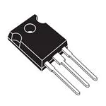
TO-247
High frequency motor controls, inverters, ups
2
TO-220
3
HF, SMPS and PFC in both hard switch and
resonant topologies
1
D²PAK
Description
This IGBT utilizes the advanced PowerMESH™
process resulting in an excellent trade-off
between switching performance and low on-state
behavior.
Table 1.
Figure 1.
Internal schematic diagram
Device summary
Order codes
Marking
Package
Packaging
STGB30NC60WT4
GB30NC60W
D²PAK
Tape and reel
STGP30NC60W
GP30NC60W
TO-220
Tube
STGW30NC60W
GW30NC60W
TO-247
Tube
March 2008
Rev 8
1/16
www.st.com
16
�Contents
STGB30NC60WT4 - STGP30NC60W - STGW30NC60W
Contents
1
Electrical ratings . . . . . . . . . . . . . . . . . . . . . . . . . . . . . . . . . . . . . . . . . . . . 3
2
Electrical characteristics . . . . . . . . . . . . . . . . . . . . . . . . . . . . . . . . . . . . . 4
2.1
Electrical characteristics (curves)
............................. 5
3
Test circuit
4
Package mechanical data . . . . . . . . . . . . . . . . . . . . . . . . . . . . . . . . . . . . . 9
5
Packaging mechanical data . . . . . . . . . . . . . . . . . . . . . . . . . . . . . . . . . . 13
6
Revision history . . . . . . . . . . . . . . . . . . . . . . . . . . . . . . . . . . . . . . . . . . . 14
2/16
................................................ 8
�STGB30NC60WT4 - STGP30NC60W - STGW30NC60W
1
Electrical ratings
Electrical ratings
Table 2.
Absolute maximum ratings
Symbol
Parameter
Value
Unit
VCES
Collector-emitter voltage (VGE = 0)
600
V
IC (1)
Collector current (continuous) at 25 °C
60
A
IC (1)
Collector current (continuous) at 100 °C
30
A
ICL(2)
Turn-off latching current
150
A
ICP (3)
Pulsed collector current
150
A
VGE
Gate-emitter voltage
± 20
V
PTOT
Total dissipation at TC = 25 °C
200
W
Tj
Operating junction temperature
– 55 to 150
°C
1. Calculated according to the iterative formula:
T
–T
JMAX
C
I ( T ) = ----------------------------------------------------------------------------------------------------C C
R
× V
(T , I )
THJ – C
CESAT ( MAX ) C C
2. Vclamp = 80%(VCES), Tj =150 °C, RG=10 Ω, VGE=15 V
3. Pulse width limited by max junction temperature allowed
Table 3.
Thermal resistance
Value
Symbol
Parameter
TO-247
Rthj-case
Thermal resistance junction-case max
Rthj-amb
Thermal resistance junction-ambient max
TO-220
D²PAK
0.62
50
Unit
°C/W
62.5
°C/W
3/16
�Electrical characteristics
2
STGB30NC60WT4 - STGP30NC60W - STGW30NC60W
Electrical characteristics
(TCASE=25°C unless otherwise specified)
Table 4.
Symbol
Static electrical characteristics
Parameter
Collector-emitter
V(BR)CES breakdown voltage
(VGE = 0)
Test conditions
IC = 1 mA
VCE(sat)
Collector-emitter saturation VGE=15 V, IC= 20 A
voltage
VGE=15 V, IC= 20 A,Tc= 125 °C
VGE(th)
Gate threshold voltage
VCE= VGE, IC= 250 µA
ICES
Collector cut-off current
(VGE = 0)
VCE = 600 V
IGES
Gate-emitter leakage
current (VCE = 0)
VGE = ±20 V
gfs (1)
Forward transconductance
VCE = 15 V, IC= 20 A
Min.
Typ.
Max.
600
Unit
V
2.1
1.8
3.75
VCE = 600 V, Tc=125 °C
2.5
V
V
5.75
V
10
1
µA
mA
± 100
nA
15
S
1. Pulse duration = 300 µs, duty cycle 1.5%
Table 5.
Symbol
Cies
Coes
Cres
Qg
Qge
Qgc
4/16
Dynamic electrical characteristics
Parameter
Test conditions
Input capacitance
Output capacitance
Reverse transfer
capacitance
VCE = 25 V, f = 1 MHz,
VGE=0
Total gate charge
Gate-emitter charge
Gate-collector charge
VCE = 390 V, IC = 20 A,
VGE = 15 V,
(see Figure 17)
Min.
Typ.
Max.
Unit
2080
175
52
pF
pF
pF
102
17.5
47
nC
nC
nC
�STGB30NC60WT4 - STGP30NC60W - STGW30NC60W
Table 6.
Symbol
td(on)
tr
(di/dt)on
td(on)
tr
(di/dt)on
tr(Voff)
td(off)
tf
tr(Voff)
td(off)
tf
Table 7.
Symbol
Eon
Eoff(1)
Ets
Eon
Eoff(1)
Ets
Electrical characteristics
Switching on/off (inductive load)
Parameter
Test conditions
Turn-on delay time
Current rise time
Turn-on current slope
VCC = 390 V, IC = 20 A
Turn-on delay time
Current rise time
Turn-on current slope
VCC = 390 V, IC = 20 A
Off voltage rise time
Turn-off delay time
Current fall time
Vcc = 390 V, IC = 20 A,
Off voltage rise time
Turn-off delay time
Current fall time
Vcc = 390 V, IC = 20 A,
Min.
RG= 10 Ω, VGE= 15 V,
(see Figure 16)
RG= 10 Ω, VGE= 15 V,
TC= 125 °C (see Figure 16)
RG = 10 Ω, VGE = 15 V
(see Figure 18)
RG=10 Ω, VGE =15 V,
TC=125 °C (see Figure 18)
Typ.
Max.
Unit
29.5
12
1640
ns
ns
A/µs
29
13.5
1600
ns
ns
A/µs
19.5
118
27
ns
ns
ns
46
151
38
ns
ns
ns
Switching energy (inductive load)
Parameter
Test conditions
Turn-on switching losses
Turn-off switching losses
Total switching losses
VCC = 390 V, IC = 20 A
Turn-on switching losses
Turn-off switching losses
Total switching losses
VCC = 390 V, IC = 20 A
RG= 10 Ω, VGE= 15 V,
(see Figure 18)
RG= 10 Ω, VGE= 15 V,
TC= 125 °C (see Figure 18)
Min.
Typ.
Max.
Unit
305
181
486
µJ
µJ
µJ
455
355
801
µJ
µJ
µJ
1. Turn-off losses include also the tail of the collector current
5/16
�Electrical characteristics
STGB30NC60WT4 - STGP30NC60W - STGW30NC60W
2.1
Electrical characteristics (curves)
Figure 2.
Output characteristics
Figure 3.
Transfer characteristics
Figure 4.
Transconductance
Figure 5.
Collector-emitter on voltage vs
temperature
HV28940
VCE(V)
VGE=15V
3.2
3
40A
30A
2.8
20A
2.6
2.4
2.2
2
1.8
IC=10A
1.6
1.4
-75
Figure 6.
6/16
Gate charge vs gate-source voltage Figure 7.
-50
-25
0
25
50
75
100 125 150 TJ(°C)
Capacitance variations
�STGB30NC60WT4 - STGP30NC60W - STGW30NC60W
Figure 8.
Normalized gate threshold voltage
vs temperature
Electrical characteristics
Figure 9.
Collector-emitter on voltage vs
collector current
HV28950
VCE (V)
3.4
3.2
TJ=-50°C
3
TJ=25°C
2.8
2.6
2.4
2.2
TJ=150°C
2
1.8
1.6
1.4
1.2
1
0.8
0
Figure 10. Normalized breakdown voltage vs
temperature
5
10 15 20 25 30 35 40 45 50 55 60 IC(A)
Figure 11. Switching losses vs temperature
Figure 12. Switching losses vs gate resistance Figure 13. Switching losses vs collector
current
7/16
�Electrical characteristics
Figure 14. Thermal impedance
8/16
STGB30NC60WT4 - STGP30NC60W - STGW30NC60W
Figure 15. Turn-off SOA
�STGB30NC60WT4 - STGP30NC60W - STGW30NC60W
3
Test circuit
Test circuit
Figure 16. Test circuit for inductive load
switching
Figure 17. Gate charge test circuit
Figure 18. Switching waveform
9/16
�Package mechanical data
4
STGB30NC60WT4 - STGP30NC60W - STGW30NC60W
Package mechanical data
In order to meet environmental requirements, ST offers these devices in ECOPACK®
packages. These packages have a lead-free second level interconnect. The category of
second level interconnect is marked on the package and on the inner box label, in
compliance with JEDEC Standard JESD97. The maximum ratings related to soldering
conditions are also marked on the inner box label. ECOPACK is an ST trademark.
ECOPACK specifications are available at: www.st.com
10/16
�STGB30NC60WT4 - STGP30NC60W - STGW30NC60W
Package mechanical data
TO-220 mechanical data
mm
inch
Dim
Min
A
b
b1
c
D
D1
E
e
e1
F
H1
J1
L
L1
L20
L30
∅P
Q
Typ
4.40
0.61
1.14
0.48
15.25
Max
Min
4.60
0.88
1.70
0.70
15.75
0.173
0.024
0.044
0.019
0.6
10.40
2.70
5.15
1.32
6.60
2.72
14
3.93
0.393
0.094
0.194
0.048
0.244
0.094
0.511
0.137
1.27
10
2.40
4.95
1.23
6.20
2.40
13
3.50
Max
0.181
0.034
0.066
0.027
0.62
0.050
16.40
28.90
3.75
2.65
Typ
0.409
0.106
0.202
0.051
0.256
0.107
0.551
0.154
0.645
1.137
3.85
2.95
0.147
0.104
0.151
0.116
11/16
�Package mechanical data
STGB30NC60WT4 - STGP30NC60W - STGW30NC60W
TO-247 Mechanical data
mm.
Dim.
A
Min.
4.85
A1
2.20
2.60
b
1.0
1.40
b1
2.0
2.40
b2
3.0
3.40
Max.
5.15
c
0.40
0.80
D
19.85
20.15
E
15.45
15.75
e
5.45
L
14.20
14.80
L1
3.70
4.30
L2
18.50
øP
3.55
øR
4.50
S
12/16
Typ
3.65
5.50
5.50
�STGB30NC60WT4 - STGP30NC60W - STGW30NC60W
Package mechanical data
D²PAK (TO-263) mechanical data
mm
inch
Dim
Min
A
A1
b
b2
c
c2
D
D1
E
E1
e
e1
H
J1
L
L1
L2
R
V2
Typ
4.40
0.03
0.70
1.14
0.45
1.23
8.95
7.50
10
8.50
Max
Min
4.60
0.23
0.93
1.70
0.60
1.36
9.35
0.173
0.001
0.027
0.045
0.017
0.048
0.352
0.295
0.394
0.334
10.40
2.54
4.88
15
2.49
2.29
1.27
1.30
Max
0.181
0.009
0.037
0.067
0.024
0.053
0.368
0.409
0.1
5.28
15.85
2.69
2.79
1.40
1.75
0.192
0.590
0.099
0.090
0.05
0.051
8°
0°
0.4
0°
Typ
0.208
0.624
0.106
0.110
0.055
0.069
0.016
8°
0079457_M
13/16
�Packaging mechanical data
5
STGB30NC60WT4 - STGP30NC60W - STGW30NC60W
Packaging mechanical data
D2PAK FOOTPRINT
TAPE AND REEL SHIPMENT
REEL MECHANICAL DATA
DIM.
mm
MIN.
A
B
1.5
C
12.8
D
20.2
G
24.4
N
100
T
TAPE MECHANICAL DATA
DIM.
mm
MIN.
MAX.
MIN.
A0
10.5
10.7
0.413 0.421
B0
15.7
15.9
0.618 0.626
D
1.5
1.6
0.059 0.063
D1
1.59
1.61
0.062 0.063
E
1.65
1.85
0.065 0.073
F
11.4
11.6
0.449 0.456
K0
4.8
5.0
0.189 0.197
P0
3.9
4.1
0.153 0.161
P1
11.9
12.1
0.468 0.476
P2
1.9
2.1
0.075 0.082
MAX.
R
50
1.574
T
0.25
0.35 0.0098 0.0137
W
23.7
24.3
* on sales type
14/16
inch
0.933 0.956
inch
MAX.
MIN.
MAX.
330
12.992
13.2
0.504 0.520
26.4
0.960 1.039
0.059
0795
3.937
30.4
1.197
BASE QTY
BULK QTY
1000
1000
�STGB30NC60WT4 - STGP30NC60W - STGW30NC60W
6
Revision history
Revision history
Table 8.
Document revision history
Date
Revision
Changes
15-Sep-2005
1
Initial release.
04-Jan-2006
2
Inserted TO-220. Complete version
18-Dec-2006
3
The document has been reformatted
15-Feb-2007
4
Mechanical data TO-220 has been updated
26-Mar-2007
5
Typo mistake on page 1
12-Jul-2007
6
Corrected Figure 11, Figure 12, Figure 13
04-Oct-2007
7
Symbol on Table 4 has been corrected
17-Mar-2008
8
Figure 5 and Figure 9 have been updated
Inserted device in D2PAK
15/16
�STGB30NC60WT4 - STGP30NC60W - STGW30NC60W
Please Read Carefully:
Information in this document is provided solely in connection with ST products. STMicroelectronics NV and its subsidiaries (“ST”) reserve the
right to make changes, corrections, modifications or improvements, to this document, and the products and services described herein at any
time, without notice.
All ST products are sold pursuant to ST’s terms and conditions of sale.
Purchasers are solely responsible for the choice, selection and use of the ST products and services described herein, and ST assumes no
liability whatsoever relating to the choice, selection or use of the ST products and services described herein.
No license, express or implied, by estoppel or otherwise, to any intellectual property rights is granted under this document. If any part of this
document refers to any third party products or services it shall not be deemed a license grant by ST for the use of such third party products
or services, or any intellectual property contained therein or considered as a warranty covering the use in any manner whatsoever of such
third party products or services or any intellectual property contained therein.
UNLESS OTHERWISE SET FORTH IN ST’S TERMS AND CONDITIONS OF SALE ST DISCLAIMS ANY EXPRESS OR IMPLIED
WARRANTY WITH RESPECT TO THE USE AND/OR SALE OF ST PRODUCTS INCLUDING WITHOUT LIMITATION IMPLIED
WARRANTIES OF MERCHANTABILITY, FITNESS FOR A PARTICULAR PURPOSE (AND THEIR EQUIVALENTS UNDER THE LAWS
OF ANY JURISDICTION), OR INFRINGEMENT OF ANY PATENT, COPYRIGHT OR OTHER INTELLECTUAL PROPERTY RIGHT.
UNLESS EXPRESSLY APPROVED IN WRITING BY AN AUTHORIZED ST REPRESENTATIVE, ST PRODUCTS ARE NOT
RECOMMENDED, AUTHORIZED OR WARRANTED FOR USE IN MILITARY, AIR CRAFT, SPACE, LIFE SAVING, OR LIFE SUSTAINING
APPLICATIONS, NOR IN PRODUCTS OR SYSTEMS WHERE FAILURE OR MALFUNCTION MAY RESULT IN PERSONAL INJURY,
DEATH, OR SEVERE PROPERTY OR ENVIRONMENTAL DAMAGE. ST PRODUCTS WHICH ARE NOT SPECIFIED AS "AUTOMOTIVE
GRADE" MAY ONLY BE USED IN AUTOMOTIVE APPLICATIONS AT USER’S OWN RISK.
Resale of ST products with provisions different from the statements and/or technical features set forth in this document shall immediately void
any warranty granted by ST for the ST product or service described herein and shall not create or extend in any manner whatsoever, any
liability of ST.
ST and the ST logo are trademarks or registered trademarks of ST in various countries.
Information in this document supersedes and replaces all information previously supplied.
The ST logo is a registered trademark of STMicroelectronics. All other names are the property of their respective owners.
© 2008 STMicroelectronics - All rights reserved
STMicroelectronics group of companies
Australia - Belgium - Brazil - Canada - China - Czech Republic - Finland - France - Germany - Hong Kong - India - Israel - Italy - Japan Malaysia - Malta - Morocco - Singapore - Spain - Sweden - Switzerland - United Kingdom - United States of America
www.st.com
16/16
�


 工商网监
湘ICP备2023018690号
工商网监
湘ICP备2023018690号
