STGW40H65DFB-4
Datasheet
Trench gate field-stop 650 V, 40 A high speed HB series IGBT
Features
1
2
4
3
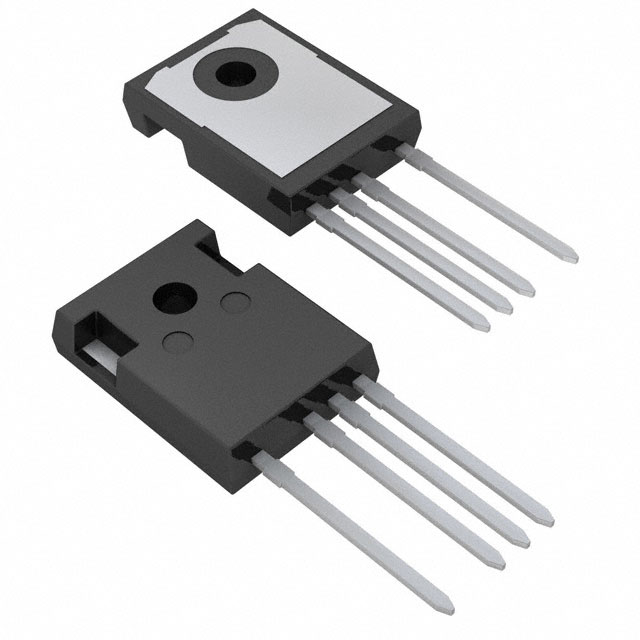
TO247-4
C(1, TAB)
•
Maximum junction temperature: TJ = 175 °C
•
•
•
High speed switching series
Minimized tail current
Low saturation voltage: VCE(sat) = 1.6 V (typ.) @ IC = 40 A
•
•
•
Tight parameter distribution
Safe paralleling
Positive VCE(sat) temperature coefficient
•
•
•
Low thermal resistance
Very fast soft recovery antiparallel diode
Excellent switching performance thanks to the extra driving kelvin pin
G(4)
Applications
K(3)
E(2)
NG4K3E2C1_TAB
•
•
Photovoltaic inverters
High frequency converters
Description
This device is an IGBT developed using an advanced proprietary trench gate fieldstop structure. The device is part of the new HB series of IGBTs, which represents an
optimum compromise between conduction and switching loss to maximize the
efficiency of any frequency converter. A faster switching event can be achieved by
the Kelvin pin, which separates power path from driving signal. Furthermore, the
slightly positive VCE(sat) temperature coefficient and very tight parameter distribution
result in safer paralleling operation.
Product status link
STGW40H65DFB-4
Product summary
Order code
STGW40H65DFB-4
Marking
G40H65DFB
Package
TO247-4
Packing
Tube
DS11520 - Rev 4 - June 2019
For further information contact your local STMicroelectronics sales office.
www.st.com
�STGW40H65DFB-4
Electrical ratings
1
Electrical ratings
Table 1. Absolute maximum ratings
Symbol
Value
Unit
Collector-emitter voltage (VGE = 0 V)
650
V
Continuous collector current at TC = 25 °C
80
Continuous collector current at TC = 100 °C
40
Pulsed collector current
160
Gate-emitter voltage
±20
Transient gate-emitter voltage
±30
Continuous forward current at TC = 25 °C
80
Continuous forward current at TC = 100 °C
40
IFP (1)
Pulsed forward current
160
A
PTOT
Total power dissipation at TC = 25 °C
283
W
TSTG
Storage temperature range
- 55 to 150
Operating junction temperature range
- 55 to 175
VCES
IC
ICP (1)
VGE
IF
TJ
Parameter
A
A
V
A
°C
1. Pulse width limited by maximum junction temperature.
Table 2. Thermal data
Symbol
DS11520 - Rev 4
Parameter
Value
RthJC
Thermal resistance junction-case IGBT
0.53
RthJC
Thermal resistance junction-case diode
1.14
RthJA
Thermal resistance junction-ambient
Unit
°C/W
50
page 2/15
�STGW40H65DFB-4
Electrical characteristics
2
Electrical characteristics
TC = 25 °C unless otherwise specified
Table 3. Static characteristics
Symbol
Parameter
V(BR)CES
Collector-emitter
breakdown voltage
VCE(sat)
VF
Collector-emitter
saturation voltage
Forward on-voltage
Test conditions
VGE = 0 V, IC = 2 mA
Min.
Typ.
650
1.6
VGE = 15 V, IC = 40 A,
TJ = 125 °C
1.7
VGE = 15 V, IC = 40 A,
TJ = 175 °C
1.8
IF = 40 A
1.7
IF = 40 A, TJ = 125 °C
1.4
IF = 40 A, TJ = 175 °C
1.3
Gate threshold voltage
VCE = VGE, IC = 1 mA
ICES
Collector cut-off current
IGES
Gate-emitter leakage
current
5
Unit
V
VGE = 15 V, IC = 40 A
VGE(th)
Max.
6
2
V
2.45
V
7
V
VGE = 0 V, VCE = 650 V
25
µA
VCE = 0 V, VGE = ±20 V
±250
µA
Unit
Table 4. Dynamic characteristics
Symbol
DS11520 - Rev 4
Parameter
Cies
Input capacitance
Coes
Output capacitance
Cres
Reverse transfer
capacitance
Qg
Total gate charge
Qge
Gate-emitter charge
Qgc
Gate-collector charge
Test conditions
VCE = 25 V, f = 1 MHz, VGE = 0 V
VCC = 520 V, IC = 40 A, VGE = 0
to 15 V
(see Figure 29. Gate charge test
circuit)
Min.
Typ.
Max.
-
5412
-
-
198
-
-
107
-
-
210
-
-
39
-
-
82
-
pF
nC
page 3/15
�STGW40H65DFB-4
Electrical characteristics
Table 5. IGBT switching characteristics (inductive load)
Symbol
td(on)
tr
(di/dt)on
td(off)
tf
Parameter
Test conditions
Min.
Typ.
Max.
Unit
Turn-on delay time
-
40
-
ns
Current rise time
-
13
-
ns
-
2553
-
A/µs
-
142
-
ns
-
26
-
ns
-
200
-
µJ
Turn-on current slope
Turn-off-delay time
Current fall time
VCE = 400 V, IC = 40 A,
VGE = 15 V, RG = 5 Ω
(see Figure 28. Test circuit for
inductive load switching)
(1)
Turn-on switching energy
Eoff (2)
Turn-off switching energy
-
410
-
µJ
Total switching energy
-
610
-
µJ
Turn-on delay time
-
40
-
ns
Current rise time
-
14.8
-
ns
Eon
Ets
td(on)
tr
(di/dt)on
td(off)
tf
Turn-on current slope
VCE = 400 V, IC = 40 A,
-
2216
-
A/µs
Turn-off-delay time
VGE = 15 V, RG = 5 Ω,
TJ = 175 °C
(see Figure 28. Test circuit for
inductive load switching)
-
148
-
ns
-
61
-
ns
-
472
-
µJ
Current fall time
Eon (1)
Turn-on switching energy
(2)
Turn-off switching energy
-
816
-
µJ
Total switching energy
-
1288
-
µJ
Eoff
Ets
1. Including the reverse recovery of the diode.
2. Including the tail of the collector current.
Table 6. Diode switching characteristics (inductive load)
Symbol
DS11520 - Rev 4
Parameter
Test conditions
Min.
Typ.
Max.
Unit
-
62
-
ns
-
99
-
nC
-
3.3
-
A
-
187
-
A/µs
trr
Reverse recovery time
Qrr
Reverse recovery charge
Irrm
Reverse recovery current
dIrr/dt
Peak rate of fall of
reverse recovery current
during tb
Err
Reverse recovery energy
-
68
-
µJ
trr
Reverse recovery time
-
310
-
ns
Qrr
Reverse recovery charge
IF = 40 A, VR = 400 V,
-
1550
-
nC
Irrm
Reverse recovery current
-
10
-
A
dIrr/dt
Peak rate of fall of
reverse recovery current
during tb
VGE = 15 V, TJ = 175 °C,
di/dt = 100 A/µs (see Figure 28.
Test circuit for inductive load
switching)
-
70
-
A/µs
Err
Reverse recovery energy
-
674
-
µJ
IF = 40 A, VR = 400 V,
VGE = 15 V,
di/dt = 100 A/µs (see Figure 28.
Test circuit for inductive load
switching)
page 4/15
�STGW40H65DFB-4
Electrical characteristics (curves)
2.1
Electrical characteristics (curves)
Figure 1. Power dissipation vs case temperature
PTOT
(W)
IGBT230216EWF6GPDT
VGE = 15 V, TJ ≤ 175 °C
250
Figure 2. Collector current vs case temperature
IC
(A)
IGBT230216EWF6GCCT
VGE = 15 V, TJ ≤ 175 °C
80
200
60
150
40
100
20
50
0
0
25
50
75
100
125
150
TC (°C)
Figure 3. Output characteristics (TJ = 25 °C)
IC
(A)
IGBT230216EWF6GOC25
VGE = 15 V
140
0
0
11 V
80
IC
(A)
125
40
40
20
20
2
3
4
VCE (V)
Figure 5. VCE(sat) vs junction temperature
VCE(SAT)
(V)
IGBT230216EWF6GVCET
VGE = 15 V
TC (°C)
IGBT230216EWF6GOC175
VGE = 15 V
13 V
11 V
9V
80
9V
1
150
100
60
IC = 80 A
7V
0
0
1
2
3
4
VCE (V)
Figure 6. VCE(sat) vs collector current
VCE(SAT)
(V)
2.4
IGBT230216EWF6GVCEC
VGE = 15 V
TJ = 175 °C
2.2
2.2
2.0
2.0
TJ = 25 °C
1.8
IC = 40 A
1.8
1.6
1.6
TJ = -40 °C
1.4
1.4
DS11520 - Rev 4
100
Figure 4. Output characteristics (TJ = 175 °C)
60
1.2
-75
75
120
100
2.4
50
140
13 V
120
0
0
25
1.2
IC = 20 A
-25
25
75
125
175
TJ (°C)
1.0
0
10
20
30
40
50
60
70
IC (A)
page 5/15
�STGW40H65DFB-4
Electrical characteristics (curves)
Figure 7. Collector current vs switching frequency
IC
(A)
IGBT230216EWF6GCCS
Figure 8. Forward bias safe operating area
IC
(A)
IGBT230216EWF6GFSOA
100
80
10 2
TC = 80 °C
60
TC = 100 °C
tp = 10 µs
10 1
40
tp = 100 µs
20
Rectangular current shape
(duty cycle = 0.5, VCC = 400 V
RG = 5 Ω, VGE = 0/15 V , TJ = 175 °C
0
10 0
10 1
f (kHz)
10 2
Figure 9. Transfer characteristics
IC
(A)
140
IGBT230216EWF6GTCH
VCE = 5 V
TJ = 175 °C
100
80
60
10 1
tp = 1 ms
VCE (V)
10 2
Figure 10. Diode VF vs forward current
VF
(V)
IGBT230216EWF6GDVF
TJ = -40 °C
2.3
TJ = 25 °C
120
single pulse, TC = 25°C
TJ ≤ 175 °C, VGE = 15 V
10 0
10 0
2.0
TJ = 25 °C
1.7
TJ = 175 °C
TJ = 175 °C
1.4
40
TJ = 25 °C
20
0
6
7
8
9
1.1
10
VGE (V)
Figure 11. Normalized VGE(th) vs junction temperature
VGE(th)
(Norm.)
IGBT230216EWF6GNVGE
30
40
50
60
70
80
IF (A)
Figure 12. Normalized V(BR)CES vs junction temperature
V(BR)CES
(Norm.)
IGBT230216EWF6GNVBR
IC = 2 mA
1.12
VCE = VGE , IC = 1 mA
1.2
0.8
20
1.08
1.0
1.04
1.00
0.8
0.96
0.6
0.4
-75
DS11520 - Rev 4
0.92
-25
25
75
125
175
TJ (°C)
0.88
-75
-25
25
75
125
175
TJ (°C)
page 6/15
�STGW40H65DFB-4
Electrical characteristics (curves)
Figure 13. Capacitance variations
C
(pF)
IGBT230216EWF6GCVR
CIES
Figure 14. Gate charge vs gate-emitter voltage
VGE
(V)
IGBT230216EWF6GGCGE
VCC = 520 V, IC = 40 A
15
10 3
10
10 2
COES
5
CRES
10 1
10 -1
10 0
10 1
10 2
VCE (V)
Figure 15. Switching energy vs collector current
E
(μJ)
IGBT100320171332SLC
VGE = 15 V, TJ = 175 °C,
VCC = 400 V, RG = 5 Ω
0
0
40
80
120
160
200
Qg (nC)
Figure 16. Switching energy vs gate resistance
E
(μJ)
IGBT100320171333SLG
VGE = 15 V, TJ = 175 °C,
VCC = 400 V, IC = 40 A
1000
1500
Eoff
Eoff
1000
800
Eon
Eon
500
0
0
20
40
600
60
IC (A)
Figure 17. Switching energy vs temperature
E
(μJ)
IGBT100320171333SLT
VGE = 15 V, RG = 5 Ω,
VCC = 400 V, IC = 40 A
400
0
4
8
12
16
20
RG (Ω)
Figure 18. Switching energy vs collector emitter voltage
E
(μJ)
IGBT100320171334SLV
VGE = 15 V, RG = 5 Ω,
TJ = 175 °C, IC = 40 A
1000
700
Eoff
800
500
Eon
600
300
100
0
DS11520 - Rev 4
Eoff
Eon
400
50
100
150
TJ (°C)
200
150
300
450
VCE (V)
page 7/15
�STGW40H65DFB-4
Electrical characteristics (curves)
Figure 19. Switching times vs collector current
t
(ns)
IGBT100320171334STC
Figure 20. Switching times vs gate resistance
IGBT100320171335STR
t
(ns) V = 400 V, V = 15 V,
CC
GE
IC = 40 A, TJ = 175 °C
td(off)
10 2
td(off)
tf
10 2
td(on)
tf
10 1
tr
td(on)
10 0
VCC = 400 V, VGE = 15 V,
RG = 5 Ω, TJ = 175 °C
20
40
60
0
tr
IC (A)
Figure 21. Reverse recovery current vs diode current
slope
Irrm
(A)
IGBT230216EWF6GRRC
Vr = 400 V, IF = 40 A
10 1
0
4
8
trr
(ns)
RG (Ω)
IGBT230216EWF6GRRT
Vr = 400 V, IF = 40 A
200
150
40
TJ = 25 °C
TJ = 175 °C
100
20
TJ = 25 °C
50
0
0
500
1000 1500 2000 2500
di/dt (A/µs)
Figure 23. Reverse recovery charge vs diode current
slope
Qrr
(nC)
IGBT230216EWF6GRRQ
Vr = 400 V, IF = 40 A
4000
0
0
500
1000 1500 2000 2500
di/dt (A/µs)
Figure 24. Reverse recovery energy vs diode current
slope
Err
(µJ)
IGBT230216EWF6GRRE
Vr = 400 V, IF = 40 A
1200
TJ = 175 °C
3000
900
2000
TJ = 175 °C
600
300
TJ = 25 °C
0
0
DS11520 - Rev 4
20
250
TJ = 175 °C
60
1000
16
Figure 22. Reverse recovery time vs diode current slope
300
80
12
500
1000 1500 2000 2500
di/dt (A/µs)
0
0
TJ = 25 °C
500
1000 1500 2000 2500
di/dt (A/µs)
page 8/15
�STGW40H65DFB-4
Electrical characteristics (curves)
Figure 25. Thermal impedance for IGBT
K
ZthTO2T_A
δ = 0.5
δ = 0.2
δ = 0.05
δ = 0.1
δ = 0.02
10 -1
δ = 0.01
Single pulse
10 -2
10 -5
10 -4
10 -3
10 -2
10 -1
tp (s)
Figure 26. Thermal impedance for diode
DS11520 - Rev 4
page 9/15
�STGW40H65DFB-4
Test circuits
3
Test circuits
Figure 27. Test circuit for inductive load switching
Figure 28. Gate charge test circuit
VCC
A
A
12 V
C
47 kΩ
L=100 μH
G
E
1 kΩ
100 nF
B
B
3.3
μF
C
G
1000
μF
VCC
Vi ≤ V
D.U.T
RG
K
GMAX
2200
µF
IG=CONST
D.U.T.
100 Ω
2.7 kΩ
VG
E
47 kΩ
PW
GND1
(signal ground)
GND2
(power ground)
1 kΩ
HB650_4_leads
GIPG030320161351SA
GND1
(signal ground)
GND2
(power ground)
Figure 30. Diode reverse recovery waveform
Figure 29. Switching waveform
90%
10%
VG
90%
VCE
10%
tr(Voff)
10
tcross
90%
IC
td(on)
ton
td(off)
tr(Ion)
10%
tf
toff
AM01506v1
GADG140820170937SA
DS11520 - Rev 4
page 10/15
�STGW40H65DFB-4
Package information
4
Package information
In order to meet environmental requirements, ST offers these devices in different grades of ECOPACK packages,
depending on their level of environmental compliance. ECOPACK specifications, grade definitions and product
status are available at: www.st.com. ECOPACK is an ST trademark.
4.1
TO247-4 package information
Figure 31. TO247-4 package outline
8405626_2
DS11520 - Rev 4
page 11/15
�STGW40H65DFB-4
TO247-4 package information
Table 7. TO247-4 mechanical data
Dim.
mm
Min.
Typ.
Max.
A
4.90
5.00
5.10
A1
2.31
2.41
2.51
A2
1.90
2.00
2.10
b
1.16
b1
1.15
b2
0
0.20
c
0.59
0.66
c1
0.58
0.60
0.62
D
20.90
21.00
21.10
D1
16.25
16.55
16.85
D2
1.05
1.20
1.35
D3
24.97
25.12
25.27
E
15.70
15.80
15.90
E1
13.10
13.30
13.50
E2
4.90
5.00
5.10
E3
2.40
2.50
2.60
e
2.44
2.54
2.64
e1
4.98
5.08
5.18
L
19.80
19.92
20.10
P
3.50
3.60
3.70
1.29
1.20
P1
7.40
P2
2.40
Q
5.60
S
DS11520 - Rev 4
1.25
2.50
2.60
6.00
6.15
T
9.80
10.20
U
6.00
6.40
page 12/15
�STGW40H65DFB-4
Revision history
Table 8. Document revision history
Date
Revision
04-Mar-2016
1
Changes
First release
Updated Table 6: "IGBT switching characteristics (inductive load)".
13-Mar-2017
2
Updated Section 2.1: "Electrical characteristics (curves)".
Minor text changes
Updated title in cover page.
17-Aug-2017
3
Updated Table 7: "Diode switching characteristics (inductive load)".
Updated Section 4.1: "TO247-4 package information"
Minor text changes.
Removed maturity status indication from cover page. The document status is production data.
20-Jun-2019
4
Updated title in cover page.
Updated Table 1. Absolute maximum ratings.
Minor text changes.
DS11520 - Rev 4
page 13/15
�STGW40H65DFB-4
Contents
Contents
1
Electrical ratings . . . . . . . . . . . . . . . . . . . . . . . . . . . . . . . . . . . . . . . . . . . . . . . . . . . . . . . . . . . . . . . . . .2
2
Electrical characteristics. . . . . . . . . . . . . . . . . . . . . . . . . . . . . . . . . . . . . . . . . . . . . . . . . . . . . . . . . . . 3
2.1
Electrical characteristics (curves) . . . . . . . . . . . . . . . . . . . . . . . . . . . . . . . . . . . . . . . . . . . . . . . . . 4
3
Test circuits . . . . . . . . . . . . . . . . . . . . . . . . . . . . . . . . . . . . . . . . . . . . . . . . . . . . . . . . . . . . . . . . . . . . . .10
4
Package information. . . . . . . . . . . . . . . . . . . . . . . . . . . . . . . . . . . . . . . . . . . . . . . . . . . . . . . . . . . . . .11
4.1
TO247-4 package information . . . . . . . . . . . . . . . . . . . . . . . . . . . . . . . . . . . . . . . . . . . . . . . . . . . 11
Revision history . . . . . . . . . . . . . . . . . . . . . . . . . . . . . . . . . . . . . . . . . . . . . . . . . . . . . . . . . . . . . . . . . . . . . . .13
DS11520 - Rev 4
page 14/15
�STGW40H65DFB-4
IMPORTANT NOTICE – PLEASE READ CAREFULLY
STMicroelectronics NV and its subsidiaries (“ST”) reserve the right to make changes, corrections, enhancements, modifications, and improvements to ST
products and/or to this document at any time without notice. Purchasers should obtain the latest relevant information on ST products before placing orders. ST
products are sold pursuant to ST’s terms and conditions of sale in place at the time of order acknowledgement.
Purchasers are solely responsible for the choice, selection, and use of ST products and ST assumes no liability for application assistance or the design of
Purchasers’ products.
No license, express or implied, to any intellectual property right is granted by ST herein.
Resale of ST products with provisions different from the information set forth herein shall void any warranty granted by ST for such product.
ST and the ST logo are trademarks of ST. For additional information about ST trademarks, please refer to www.st.com/trademarks. All other product or service
names are the property of their respective owners.
Information in this document supersedes and replaces information previously supplied in any prior versions of this document.
© 2019 STMicroelectronics – All rights reserved
DS11520 - Rev 4
page 15/15
�


 工商网监
湘ICP备2023018690号
工商网监
湘ICP备2023018690号
