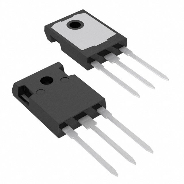
STGWA50IH65DF
Datasheet
Trench gate field-stop 650 V, 50 A, soft switching IH series IGBT
in a TO-247 long leads package
Features
C(2, TAB)
•
•
Designed for soft-commutation only
Maximum junction temperature: TJ = 175 °C
•
VCE(sat) = 1.5 V (typ.) @ IC = 50 A
•
•
•
•
•
Minimized tail current
Tight parameter distribution
Low thermal resistance
Low voltage drop freewheeling co-packaged diode
Positive VCE(sat) temperature coefficient
Applications
G(1)
•
•
•
E(3)
Induction heating
Resonant converters
Microwave ovens
NG1E3C2T
Description
The newest IGBT 650 V soft-switching IH series has been developed using an
advanced proprietary trench gate field-stop structure, whose performance is
optimized both in conduction and switching losses for soft commutation. A
freewheeling diode with a low drop forward voltage is included. The result is a
product specifically designed to maximize efficiency for any resonant and softswitching applications.
Product status link
STGWA50IH65DF
Product summary
Order code
STGWA50IH65DF
Marking
G50IH65DF
Package
TO-247 long leads
Packing
Tube
DS11796 - Rev 3 - April 2020
For further information contact your local STMicroelectronics sales office.
www.st.com
�STGWA50IH65DF
Electrical ratings
1
Electrical ratings
Table 1. Absolute maximum ratings
Symbol
Value
Unit
Collector-emitter voltage (VGE = 0 V)
650
V
Continuous collector current at TC = 25 °C
100
Continuous collector current at TC = 100 °C
50
ICP
Pulsed collector current
150
VGE
Gate-emitter voltage
±20
Continuous forward current at TC = 25 °C
50
Continuous forward current at TC = 100 °C
25
IFP(1)
Pulsed forward current
150
PTOT
Total power dissipation at TC = 25 °C
300
TSTG
Storage temperature range
- 55 to 150
Operating junction temperature range
- 55 to 175
VCES
IC
(1)
IF
TJ
Parameter
A
V
A
W
°C
1. Pulse width limited by maximum junction temperature.
Table 2. Thermal data
Symbol
RthJC
RthJA
DS11796 - Rev 3
Parameter
Value
Thermal resistance junction-case IGBT
0.5
Thermal resistance junction-case diode
1.47
Thermal resistance junction-ambient
Unit
°C/W
50
page 2/14
�STGWA50IH65DF
Electrical characteristics
2
Electrical characteristics
TC = 25 °C unless otherwise specified
Table 3. Static characteristics
Symbol
V(BR)CES
VCE(sat)
VF
Parameter
Test conditions
Collector-emitter breakdown
voltage
Collector-emitter saturation
voltage
Forward on-voltage
Typ.
Max.
VGE = 15 V, IC = 50 A
1.50
2.00
VGE = 15 V, IC = 50 A, TJ = 125 °C
1.75
VGE = 15 V, IC = 50 A, TJ = 175 °C
1.90
IF = 25 A
1.75
IF = 25 A, TJ = 125 °C
1.50
IF = 25 A, TJ = 175 °C
1.40
IF = 50 A
2.15
VGE = 0 V, IC = 250 μA
Min.
Unit
650
2.50
V
VGE(th)
Gate threshold voltage
VCE = VGE, IC = 1 mA
ICES
Collector cut-off current
VGE = 0 V, VCE = 650 V
25
µA
IGES
Gate-emitter leakage current
VCE = 0 V, VGE = ±20 V
±250
nA
Unit
5
6
7
Table 4. Dynamic characteristics
Symbol
Parameter
Cies
Input capacitance
Coes
Output capacitance
Cres
Reverse transfer capacitance
Qg
Total gate charge
Qge
Gate-emitter charge
Qgc
Gate-collector charge
Test conditions
VCE= 25 V, f = 1 MHz, VGE = 0 V
VCC = 520 V, IC = 50 A, VGE = 0 to 15 V
(see Figure 23. Gate charge test circuit)
Min.
Typ.
Max.
-
2980
-
-
150
-
-
81
-
-
158
-
-
25
-
-
72
-
Min.
Typ.
Max.
-
260
-
pF
nC
Table 5. IGBT switching characteristics (inductive load)
Symbol
td(off)
Parameter
Turn-off-delay time
Test conditions
VCC = 400 V, IC = 50 A,
VGE = 15 V, RG = 22 Ω
tf
td(off)
Current fall time
(see Figure 21. Test circuit for inductive
load switching)
-
17
-
Turn-off-delay time
VCC = 400 V, IC = 50 A,
-
270
-
-
24
-
VGE = 15 V, RG = 22 Ω, TJ = 175 °C
tf
DS11796 - Rev 3
Current fall time
(see Figure 21. Test circuit for inductive
load switching)
Unit
ns
ns
page 3/14
�STGWA50IH65DF
Electrical characteristics
Table 6. IGBT switching characteristics (snubbed inductive load)
Symbol
Parameter
Test conditions
Min.
Typ.
Max.
-
284
-
Unit
L = 100 μH, Csnub = 22 nF
VCC = 320 V, RG = 10 Ω,
IC = 50 A
Eoff (1)
Turn-off switching energy
(see Figure 22. Test circuit for snubbed
inductive load switching)
μJ
L = 100 μH, Csnub = 22 nF,
VCC = 320 V, RG = 10 Ω,
IC = 50 A, TJ = 175 °C
-
469
-
(see Figure 22. Test circuit for snubbed
inductive load switching)
1. Including the tail of the collector current.
DS11796 - Rev 3
page 4/14
�STGWA50IH65DF
Electrical characteristics (curves)
2.1
Electrical characteristics (curves)
Figure 1. Power dissipation vs case temperature
PTOT
(W)
IGBT091020171338PDT
VGE ≥ 15 V, TJ ≤ 175 °C
Figure 2. Collector current vs case temperature
IGBT051020171435CCT
IC
(A) VGE ≥ 15 V, TJ ≤ 175 °C
300
100
240
80
180
60
120
40
60
20
0
-50
0
50
100
150
TC (°C)
Figure 3. Output characteristics (TJ = 25 °C)
IC
(A)
IGBT091020171339OC25
VGE = 15 V
VGE = 11 V
125
75
IC
(A)
100
50
25
25
VGE = 7 V
2
3
4
5
VCE (V)
Figure 5. VCE(sat) vs junction temperature
VCE(sat)
(V)
2.6
IGBT051020171436VCET
VGE = 15 V
150
TC (°C)
IGBT091020171340OC175
VGE = 15 V
VGE = 11 V
VGE = 13 V
VGE = 9 V
VGE = 7 V
1
2
3
4
5
VCE (V)
Figure 6. VCE(sat) vs collector current
VCE(sat)
(V)
IGBT091020171342VCEC
VGE = 15 V
2.5
Tj = 175 °C
2.0
IC = 50 A
1.8
0
0
3.0
IC = 100 A
2.2
100
75
VGE = 9 V
1
50
Figure 4. Output characteristics (TJ = 175 °C)
50
0
0
0
125
VGE = 13 V
100
0
-50
1.5
IC = 25 A
1.4
1.0
-50
DS11796 - Rev 3
Tj = -40 °C
1.0
0
50
100
150
TJ (°C)
0.5
0
Tj = 25 °C
25
50
75
100
125
IC (A)
page 5/14
�STGWA50IH65DF
Electrical characteristics (curves)
Figure 7. Forward bias safe operating area
IC
(A)
Figure 8. Transfer characteristics
IC
(A)
IGBT051020171437FSOA
IGBT091020171435TCH
VCE = 6 V
125
tp =1 µs
102
tp =10 µs
101
101
tp =1 ms
VCE (V)
102
IGBT051020171438DVF
3.0
Tj = -40 °C
Tj = 25 °C
0
5
7
9
VGE (V)
Figure 10. Normalized VGE(th) vs junction temperature
VGE(th)
(Norm.)
IGBT091020171216NVGE
VCE = VGE , IC = 1 mA
1.0
1.8
0.9
Tj = 25 °C
1.2
0.0
0
25
1.1
2.4
0.6
Tj = 175 °C
tp =100 µs
Figure 9. Diode VF vs forward current
VF
(V)
75
50
T j ≤175 °C
T c = 25°C
V GE = 15 V
single pulse
100
100
100
0.8
Tj = 175 °C
20
40
0.7
60
80
IF (A)
0.6
-50
Figure 11. Normalized V(BR)CES vs junction temperature
V(BR)CES
(Norm.)
IGBT051020171518NVBR
0
50
100
150
Figure 12. Capacitance variations
C
(pF)
IGBT051020171519CVR
IC = 1 mA
1.06
TJ (°C)
Cies
10 3
1.02
0.98
10 2
f = 1 MHz
Coes
Cres
0.94
0.9
-50
DS11796 - Rev 3
0
50
100
150
TJ (°C)
10 1
10 -1
10 0
10 1
10 2
VCE (V)
page 6/14
�STGWA50IH65DF
Electrical characteristics (curves)
Figure 13. Gate charge vs gate-emitter voltage
IGBT051020171520GCGE
VGE
(V) VCC = 520 V, IC = 50 A, IG = 1 mA
15
12
Figure 14. Switching energy vs collector current
IGBT051020171522SLC
E
(mJ) VCC =400 V, RG = 22 Ω,
VGE = 15 V, Tj = 175 °C
2
9
Eoff
6
1
3
0
0
40
80
120
160
Qg (nC)
Figure 15. Switching energy vs temperature
E
(mJ) VCC = 400 V, IC = 50 A,
RG = 22 Ω, VGE = 15 V
IGBT051020171526SLT
0
0
30
60
90
IC (A)
Figure 16. Switching energy vs collector-emitter voltage
E
(mJ)
IGBT051020171526SLV
VGE = 15 V, Tj = 175 °C
IC = 50 A, RG = 22 Ω,
1.4
1.1
1.2
1.0
Eoff
1.0
0.9
0.8
0
Eoff
0.8
50
100
150
TJ (°C)
Figure 17. Switching times vs collector current
IGBT091020171348STC
t
(ns) VCC = 400 V, VGE = 15 V,
RG = 22 Ω, Tj = 175 °C
td(off)
0.6
150
250
350
450
VCE (V)
Figure 18. Switching energy vs snubber capacitance
IGBT101020170828SSC
Eoff
(mJ) VCC = 320 V, RG = 10 Ω,
VGE = 15 V, IC = 50 A,
L = 100 μH
0.6
10 2
TJ = 175 °C
0.4
tf
10 1
0.2
10 0
0
30
60
90
IC (A)
0
0
TJ = 25 °C
30
60
90
Csnub (nF)
tr
DS11796 - Rev 3
page 7/14
�STGWA50IH65DF
Electrical characteristics (curves)
Figure 19. Thermal impedance for IGBT
ZthTO2T_B
K
δ=0.5
0.2
0.1
0.05
-1
10
0.02
Zth=k Rthj-c
δ=tp/t
0.01
Single pulse
tp
t
-2
10 -5
10
-4
10
-3
10
-2
10
-1
10
tp (s)
Figure 20. Thermal impedance for diode
DS11796 - Rev 3
page 8/14
�STGWA50IH65DF
Test circuits
3
Test circuits
Figure 22. Test circuit for snubbed inductive load
switching
Figure 21. Test circuit for inductive load switching
C
A
A
L=100 µH
G
E
B
B
G
+
RG
3.3
µF
C
VCC
1000
µF
D.U.T
E
AM01504v1
AM17096v1
Figure 23. Gate charge test circuit
Figure 24. Switching waveform
VCC
RL
Vi ≤ VGMAX
IG = CONST
90%
10%
VG
100 Ω
D.U.T.
2200
μF
2.7 kΩ
90%
VCE
10%
tr(Voff)
tcross
90%
47 kΩ
PW
IC
td(on)
ton
1 kΩ
td(off)
tr(Ion)
10%
tf
toff
AM01506v1
GADG160420181048IG
DS11796 - Rev 3
page 9/14
�STGWA50IH65DF
Package information
4
Package information
In order to meet environmental requirements, ST offers these devices in different grades of ECOPACK packages,
depending on their level of environmental compliance. ECOPACK specifications, grade definitions and product
status are available at: www.st.com. ECOPACK is an ST trademark.
4.1
TO-247 long leads package information
Figure 25. TO-247 long leads package outline
8463846_2_F
DS11796 - Rev 3
page 10/14
�STGWA50IH65DF
TO-247 long leads package information
Table 7. TO-247 long leads package mechanical data
Dim.
mm
Min.
Typ.
Max.
A
4.90
5.00
5.10
A1
2.31
2.41
2.51
A2
1.90
2.00
2.10
b
1.16
1.26
b2
3.25
b3
2.25
c
0.59
0.66
D
20.90
21.00
21.10
E
15.70
15.80
15.90
E2
4.90
5.00
5.10
E3
2.40
2.50
2.60
e
5.34
5.44
5.54
L
19.80
19.92
20.10
L1
DS11796 - Rev 3
4.30
P
3.50
Q
5.60
S
6.05
3.60
3.70
6.00
6.15
6.25
page 11/14
�STGWA50IH65DF
Revision history
Table 8. Document revision history
Date
Revision
02-Sep-2016
1
Changes
First release.
Modified title, silhouette, features and description.
05-Oct-2017
2
Modified Table 2: "Absolute maximum ratings", Table 3: "Thermal data", Table 4: "Static
characteristics", Table 5: "Dynamic characteristics", Table 6: "IGBT switching characteristics
(inductive load)"and Table 7: "IGBT switching characteristics (snubbed inductive load)".
Added Section 2.1: "Electrical characteristics (curves)".
Minor text changes.
Updated Internal schematic in cover page.
15-Apr-2020
3
Updated Figure 13. Gate charge vs gate-emitter voltage.
Minor text changes.
DS11796 - Rev 3
page 12/14
�STGWA50IH65DF
Contents
Contents
1
Electrical ratings . . . . . . . . . . . . . . . . . . . . . . . . . . . . . . . . . . . . . . . . . . . . . . . . . . . . . . . . . . . . . . . . . .2
2
Electrical characteristics. . . . . . . . . . . . . . . . . . . . . . . . . . . . . . . . . . . . . . . . . . . . . . . . . . . . . . . . . . . 3
2.1
Electrical characteristics (curves) . . . . . . . . . . . . . . . . . . . . . . . . . . . . . . . . . . . . . . . . . . . . . . . . . 5
3
Test circuits . . . . . . . . . . . . . . . . . . . . . . . . . . . . . . . . . . . . . . . . . . . . . . . . . . . . . . . . . . . . . . . . . . . . . . .9
4
Package information. . . . . . . . . . . . . . . . . . . . . . . . . . . . . . . . . . . . . . . . . . . . . . . . . . . . . . . . . . . . . .10
4.1
TO-247 long leads package information. . . . . . . . . . . . . . . . . . . . . . . . . . . . . . . . . . . . . . . . . . . 10
Revision history . . . . . . . . . . . . . . . . . . . . . . . . . . . . . . . . . . . . . . . . . . . . . . . . . . . . . . . . . . . . . . . . . . . . . . .12
DS11796 - Rev 3
page 13/14
�STGWA50IH65DF
IMPORTANT NOTICE – PLEASE READ CAREFULLY
STMicroelectronics NV and its subsidiaries (“ST”) reserve the right to make changes, corrections, enhancements, modifications, and improvements to ST
products and/or to this document at any time without notice. Purchasers should obtain the latest relevant information on ST products before placing orders. ST
products are sold pursuant to ST’s terms and conditions of sale in place at the time of order acknowledgement.
Purchasers are solely responsible for the choice, selection, and use of ST products and ST assumes no liability for application assistance or the design of
Purchasers’ products.
No license, express or implied, to any intellectual property right is granted by ST herein.
Resale of ST products with provisions different from the information set forth herein shall void any warranty granted by ST for such product.
ST and the ST logo are trademarks of ST. For additional information about ST trademarks, please refer to www.st.com/trademarks. All other product or service
names are the property of their respective owners.
Information in this document supersedes and replaces information previously supplied in any prior versions of this document.
© 2020 STMicroelectronics – All rights reserved
DS11796 - Rev 3
page 14/14
�