STGW60V60DF, STGWA60V60DF
STGWT60V60DF
Trench gate field-stop IGBT, V series
600 V, 60 A very high speed
Datasheet - production data
Features
• Maximum junction temperature: TJ = 175 °C
• Tail-less switching off
2
3
�
1
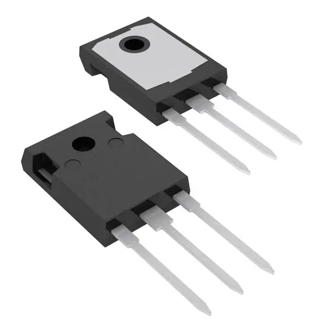
TO-247
�
�
TO-247 long leads
• VCE(sat) = 1.85 V (typ.) @ IC = 60 A
• Tight parameter distribution
• Safe paralleling
• Low thermal resistance
TAB
• Very fast soft recovery antiparallel diode
Applications
3
2
1
• Photovoltaic inverters
TO-3P
Figure 1. Internal schematic diagram
C (2 or TAB)
• Uninterruptible power supply
• Welding
• Power factor correction
• Very high frequency converters
Description
These devices are IGBTs developed using an
advanced proprietary trench gate field-stop
structure. These devices are part of the V series
of IGBTs, which represents an optimum
compromise between conduction and switching
losses to maximize the efficiency of very high
frequency converters. Furthermore, a positive
VCE(sat) temperature coefficient and very tight
parameter distribution result in safer paralleling
operation.
G (1)
E (3)
Table 1. Device summary
Order code
Marking
Package
Packing
STGW60V60DF
GW60V60DF
TO-247
Tube
STGWA60V60DF
G60V60DF
TO-247 long leads
Tube
STGWT60V60DF
GWT60V60DF
TO-3P
Tube
September 2016
This is information on a product in full production.
DocID024154 Rev 7
1/20
www.st.com
20
�Contents
STGW60V60DF, STGWA60V60DF, STGWT60V60DF
Contents
1
Electrical ratings . . . . . . . . . . . . . . . . . . . . . . . . . . . . . . . . . . . . . . . . . . . . 3
2
Electrical characteristics . . . . . . . . . . . . . . . . . . . . . . . . . . . . . . . . . . . . . 4
2.1
Electrical characteristics (curves)
............................. 6
3
Test circuits . . . . . . . . . . . . . . . . . . . . . . . . . . . . . . . . . . . . . . . . . . . . . . 11
4
Package information . . . . . . . . . . . . . . . . . . . . . . . . . . . . . . . . . . . . . . . . 12
5
2/20
4.1
TO-247 package information . . . . . . . . . . . . . . . . . . . . . . . . . . . . . . . . . . 13
4.2
TO-247 long leads package information . . . . . . . . . . . . . . . . . . . . . . . . . 15
4.3
TO-3P package information . . . . . . . . . . . . . . . . . . . . . . . . . . . . . . . . . . . 17
Revision history . . . . . . . . . . . . . . . . . . . . . . . . . . . . . . . . . . . . . . . . . . . 19
DocID024154 Rev 7
�STGW60V60DF, STGWA60V60DF, STGWT60V60DF
1
Electrical ratings
Electrical ratings
Table 2. Absolute maximum ratings
Symbol
VCES
Parameter
Collector-emitter voltage (VGE = 0)
Value
Unit
600
V
(1)
A
IC
Continuous collector current at TC = 25 °C
IC
Continuous collector current at TC = 100 °C
60
A
ICP(2)
Pulsed collector current
240
A
VGE
Gate-emitter voltage
±20
V
(1)
A
80
IF
Continuous forward current at TC = 25 °C
IF
Continuous forward current at TC = 100 °C
60
A
IFP(2)
Pulsed forward current
240
A
PTOT
Total dissipation at TC = 25 °C
375
W
TSTG
Storage temperature range
- 55 to 150
°C
Operating junction temperature range
- 55 to 175
°C
Value
Unit
TJ
80
1. Current level is limited by bond wires
2. Pulse width limited by maximum junction temperature.
Table 3. Thermal data
Symbol
Parameter
RthJC
Thermal resistance junction-case IGBT
0.4
°C/W
RthJC
Thermal resistance junction-case diode
1.14
°C/W
RthJA
Thermal resistance junction-ambient
50
°C/W
DocID024154 Rev 7
3/20
�Electrical characteristics
2
STGW60V60DF, STGWA60V60DF, STGWT60V60DF
Electrical characteristics
TJ = 25 °C unless otherwise specified.
Table 4. Static characteristics
Symbol
Parameter
Test conditions
Collector-emitter
V(BR)CES breakdown voltage
(VGE = 0)
IC = 2 mA
Min.
VGE = 15 V, IC = 60 A
Collector-emitter saturation
TJ = 125 °C
voltage
VGE = 15 V, IC = 60 A
TJ = 175 °C
Forward on-voltage
Unit
V
1.85
2.3
2.15
V
2.35
IF = 60 A
VF
Max.
600
VGE = 15 V, IC = 60 A
VCE(sat)
Typ.
2
2.6
V
IF = 60 A TJ = 125 °C
1.7
V
IF = 60 A TJ = 175 °C
1.6
V
VGE(th)
Gate threshold voltage
VCE = VGE, IC = 1 mA
ICES
Collector cut-off current
(VGE = 0)
IGES
Gate-emitter leakage
current (VCE = 0)
5
6
7
V
VCE = 600 V
25
µA
VGE = ± 20 V
±250
nA
Table 5. Dynamic characteristics
Symbol
4/20
Parameter
Cies
Input capacitance
Coes
Output capacitance
Cres
Reverse transfer
capacitance
Qg
Total gate charge
Test conditions
VCE = 25 V, f = 1 MHz,
VGE = 0
VCC = 480 V, IC = 60 A,
VGE = 15 V, see Figure 29
Qge
Gate-emitter charge
Qgc
Gate-collector charge
DocID024154 Rev 7
Min.
Typ.
Max.
Unit
-
8000
-
pF
-
280
-
pF
-
170
-
pF
-
334
-
nC
-
130
-
nC
-
58
-
nC
�STGW60V60DF, STGWA60V60DF, STGWT60V60DF
Electrical characteristics
Table 6. IGBT switching characteristics (inductive load)
Symbol
td(on)
tr
(di/dt)on
td(off)
tf
Parameter
Test conditions
Min.
Typ.
Max.
Unit
Turn-on delay time
-
60
-
ns
Current rise time
-
20
-
ns
-
2365
-
A/µs
-
208
-
ns
-
14
-
ns
Turn-on current slope
VCE = 400 V, IC = 60 A,
RG = 4.7 Ω, VGE = 15 V,
see Figure 28
Turn-off delay time
Current fall time
Eon(1)
Turn-on switching energy
-
0.75
-
mJ
Eoff(2)
Turn-off switching energy
-
0.55
-
mJ
Total switching energy
-
1.3
-
mJ
Turn-on delay time
-
57
-
ns
Current rise time
-
23
-
ns
Turn-on current slope
-
2191
-
A/µs
-
216
-
ns
-
27
-
ns
Ets
td(on)
tr
(di/dt)on
td(off)
tf
VCE = 400 V, IC = 60 A,
RG = 4.7 Ω, VGE = 15 V,
TJ = 175 °C, see Figure 28
Turn-off delay time
Current fall time
Eon(1)
Turn-on switching energy
-
1.5
-
mJ
Eoff(2)
Turn-off switching energy
-
0.8
-
mJ
Total switching energy
-
2.3
-
mJ
Ets
1. Including the reverse recovery of the diode.
2. Including the tail of the collector current.
Table 7. Diode switching characteristics (inductive load)
Symbol
Parameter
Test conditions
Min.
Typ.
Max.
Unit
-
74
-
ns
-
703
-
nC
-
19
-
A
-
714
-
A/µs
trr
Reverse recovery time
Qrr
Reverse recovery charge
Irrm
Reverse recovery current
dIrr/ /dt
Peak rate of fall of reverse
recovery current during tb
Err
Reverse recovery energy
-
184
-
µJ
trr
Reverse recovery time
-
131
-
ns
Qrr
Reverse recovery charge
-
2816
-
nC
Irrm
Reverse recovery current
-
43
-
A
dIrr/ /dt
Peak rate of fall of reverse
recovery current during tb
-
404
-
A/µs
Err
Reverse recovery energy
-
821
-
µJ
IF = 60 A, VR = 400 V,
VGE = 15 V,
diF/dt = 1000 A/µs
see Figure 28
IF = 60 A, VR = 400 V,
VGE = 15 V
diF/dt = 1000 A/µs
TJ = 175 °C, see Figure 28
DocID024154 Rev 7
5/20
�Electrical characteristics
2.1
STGW60V60DF, STGWA60V60DF, STGWT60V60DF
Electrical characteristics (curves)
Figure 2. Power dissipation vs. case
temperature
AM17139v1
Ptot (W)
Figure 3. Collector current vs. temperature case
AM17140v1
IC (A)
350
80
300
70
VGE >_ 15 V, TJ
很抱歉,暂时无法提供与“STGWA60V60DF”相匹配的价格&库存,您可以联系我们找货
免费人工找货- 国内价格
- 1+41.23347
- 3+37.15095
- 5+26.86299
- 12+25.39328
- 9000+24.57678
- 国内价格 香港价格
- 1+44.151151+5.70650
- 3+39.779753+5.14150
- 10+36.8071910+4.75730
- 30+35.1460630+4.54260
- 120+31.56151120+4.07930
- 600+30.42495600+3.93240
- 1200+29.463241200+3.80810
- 3000+27.277543000+3.52560
- 9000+26.315839000+3.40130
- 国内价格
- 1+32.77800
- 10+32.03280
- 30+31.52520