STGB30V60DF, STGP30V60DF,
STGW30V60DF, STGWT30V60DF
Trench gate field-stop IGBT, V series
600 V, 30 A very high speed
Datasheet - production data
Features
TAB
TAB
• Maximum junction temperature: TJ = 175 °C
• Tail-less switching off
3
3
1
1
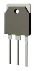
D²PAK
TO-220
2
• VCE(sat) = 1.85 V (typ.) @ IC = 30 A
• Tight parameters distribution
• Safe paralleling
TAB
• Low thermal resistance
2
3
3
• Very fast soft recovery antiparallel diode
2
1
1
Applications
TO-3P
TO-247
Figure 1. Internal schematic diagram
• Photovoltaic inverters
• Uninterruptible power supply
• Welding
C (2, TAB)
• Power factor correction
• Very high frequency converters
Description
G (1)
This device is an IGBT developed using an
advanced proprietary trench gate field stop
structure. The device is part of the V series of
IGBTs, which represent an optimum compromise
between conduction and switching losses to
maximize the efficiency of very high frequency
converters. Furthermore, a positive VCE(sat)
temperature coefficient and very tight parameter
distribution result in safer paralleling operation.
E (3)
Table 1. Device summary
Order codes
Marking
Package
Packaging
STGB30V60DF
GB30V60DF
D²PAK
Tape and reel
STGP30V60DF
GP30V60DF
TO-220
Tube
STGW30V60DF
GW30V60DF
TO-247
Tube
STGWT30V60DF
GWT30V60DF
TO-3P
Tube
October 2013
This is information on a product in full production.
DocID024361 Rev 4
1/22
www.st.com
22
�Electrical ratings
1
STGB30V60DF, STGP30V60DF, STGW30V60DF, STGWT30V60DF
Electrical ratings
Table 2. Absolute maximum ratings
Symbol
Value
Unit
Collector-emitter voltage (VGE = 0)
600
V
IC
Continuous collector current at TC = 25 °C
60
A
IC
Continuous collector current at TC = 100 °C
30
A
ICP(1)
Pulsed collector current
120
A
VGE
Gate-emitter voltage
±20
V
IF
Continuous forward current at TC = 25 °C
60
A
IF
Continuous forward current at TC = 100 °C
30
A
IFP(1)
Pulsed forward current
120
A
PTOT
Total dissipation at TC = 25 °C
258
W
TSTG
Storage temperature range
- 55 to 150
°C
Operating junction temperature
- 55 to 175
°C
Value
Unit
VCES
TJ
Parameter
1. Pulse width limited by maximum junction temperature.
Table 3. Thermal data
Symbol
2/22
Parameter
RthJC
Thermal resistance junction-case IGBT
0.58
°C/W
RthJC
Thermal resistance junction-case diode
2.08
°C/W
RthJA
Thermal resistance junction-ambient
50
°C/W
DocID024361 Rev 4
�STGB30V60DF, STGP30V60DF, STGW30V60DF, STGWT30V60DF
2
Electrical characteristics
Electrical characteristics
TJ = 25 °C unless otherwise specified.
Table 4. Static characteristics
Symbol
Parameter
Test conditions
Collector-emitter
V(BR)CES breakdown voltage
(VGE = 0)
IC = 2 mA
Min.
VGE = 15 V, IC = 30 A
Collector-emitter saturation
TJ = 125 °C
voltage
VGE = 15 V, IC = 30 A
TJ = 175 °C
Forward on-voltage
Unit
V
1.85
2.3
2.15
V
2.35
IF = 30 A
VF
Max.
600
VGE = 15 V, IC = 30 A
VCE(sat)
Typ.
2
2.6
V
IF = 30 A, TJ = 125 °C
1.7
V
IF = 30 A, TJ = 175 °C
1.6
V
VGE(th)
Gate threshold voltage
VCE = VGE, IC = 1 mA
ICES
Collector cut-off current
(VGE = 0)
IGES
Gate-emitter leakage
current (VCE = 0)
5
6
7
V
VCE = 600 V
25
μA
VGE = ± 20 V
250
nA
Table 5. Dynamic characteristics
Symbol
Parameter
Cies
Input capacitance
Coes
Output capacitance
Cres
Reverse transfer
capacitance
Qg
Total gate charge
Test conditions
VCE = 25 V, f = 1 MHz,
VGE = 0
VCC = 480 V, IC = 30 A,
VGE = 15 V, see Figure 29
Qge
Gate-emitter charge
Qgc
Gate-collector charge
DocID024361 Rev 4
Min.
Typ.
Max.
Unit
-
3750
-
pF
-
120
-
pF
-
77
-
pF
-
163
-
nC
-
28
-
nC
-
72
-
nC
3/22
�Electrical characteristics
STGB30V60DF, STGP30V60DF, STGW30V60DF, STGWT30V60DF
Table 6. IGBT switching characteristics (inductive load)
Symbol
td(on)
tr
(di/dt)on
td(off)
tf
Test conditions
Min.
Typ.
Max.
Unit
Turn-on delay time
-
45
-
ns
Current rise time
-
16
-
ns
-
1500
-
A/μs
-
189
-
ns
-
19
-
ns
Turn-on current slope
VCE = 400 V, IC = 30 A,
RG = 10 Ω, VGE = 15 V,
see Figure 28
Turn-off delay time
Current fall time
Eon(1)
Turn-on switching losses
-
383
-
μJ
Eoff(2)
Turn-off switching losses
-
233
-
μJ
Total switching losses
-
616
-
μJ
Turn-on delay time
-
42
-
ns
Current rise time
-
17
-
ns
Turn-on current slope
-
1337
-
A/μs
-
193
-
ns
-
32
-
ns
Ets
td(on)
tr
(di/dt)on
td(off)
tf
VCE = 400 V, IC = 30 A,
RG = 10 Ω, VGE = 15 V,
TJ = 175 °C, see Figure 28
Turn-off delay time
Current fall time
Eon(1)
Turn-on switching losses
-
794
-
μJ
Eoff(2)
Turn-off switching losses
-
378
-
μJ
Total switching losses
-
1172
-
μJ
Ets
1.
Parameter
Energy losses include reverse recovery of the diode.
2. Turn-off losses include also the tail of the collector current.
Table 7. Diode switching characteristics (inductive load)
Symbol
4/22
Parameter
Test conditions
Min.
Typ.
Max.
Unit
-
53
-
ns
-
384
-
nC
-
14.5
-
A
-
788
-
A/μs
trr
Reverse recovery time
Qrr
Reverse recovery charge
Irrm
Reverse recovery current
dIrr/ /dt
Peak rate of fall of reverse
recovery current during tb
Err
Reverse recovery energy
-
104
-
μJ
trr
Reverse recovery time
-
104
-
ns
Qrr
Reverse recovery charge
-
1352
-
nC
Irrm
Reverse recovery current
-
26
-
A
dIrr/ /dt
Peak rate of fall of reverse
recovery current during tb
-
310
-
A/μs
Err
Reverse recovery energy
-
407
-
μJ
IF = 30 A, VR = 400 V,
di/dt=1000 A/μs,
VGE = 15 V,
(see Figure 28)
IF = 30 A, VR = 400 V,
di/dt=1000 A/μs,
VGE = 15 V,
TJ = 175 °C, (see Figure 28)
DocID024361 Rev 4
�STGB30V60DF, STGP30V60DF, STGW30V60DF, STGWT30V60DF
2.1
Electrical characteristics
Electrical characteristics (curves)
Figure 2. Power dissipation vs. case
temperature
AM17409v1
Ptot
(W)
Figure 3. Collector current vs. case temperature
AM17410v1
IC (A)
60
250
50
200
40
150
30
100
20
50
0
0
10
25
50
0
0
75 100 125 150 175 TC(°C)
Figure 4. Output characteristics (TJ=25°C)
25
50
75 100 125 150 175
Figure 5. Output characteristics (TJ=175°C)
AM17411v1
IC (A)
120
VGE=15V
100
AM17412v1
IC (A)
120
13V
VGE=15V
13V
100
11V
80
80
60
60
9V
40
20
TC(°C)
11V
9V
40
20
7V
0
0
1
2
3
VCE(V)
4
Figure 6. VCE(sat) vs. junction temperature
AM17413v1
VCE(sat) (V)
3.2
VGE=15V
IC=60A
3.0
1
3
2
4
VCE(V)
Figure 7. VCE(sat) vs. collector current
VCE(sat) (V)
3.2
3.0
AM17414v1
Tj=175°C
VGE=15V
2.8
2.6
2.8
2.6
IC=30A
2.4
2.2
2.0
IC=15A
1.8
1.6
1.4
1.2
-50
0
0
0
50
100
150
TC(°C)
Tj=25°C
2.4
2.2
2.0
1.8
1.6
1.4
1.2
1.0
0.8
0
DocID024361 Rev 4
Tj=-40°C
10
20
30
40
50
60 IC(A)
5/22
�Electrical characteristics
STGB30V60DF, STGP30V60DF, STGW30V60DF, STGWT30V60DF
Figure 8. Collector current vs. switching
frequency
Figure 9. Forward bias safe operating area
AM17415v1
80
TC=80°C
100
70
60
AM17416v1
IC (A)
IC (A)
10μs
TC=100°C
10
50
1ms
40
1
30
20
10
100μs
0.1
rectangular current shape,
(duty cycle=0.5, Vcc= 400V Rg=10Ω,
Vge=0/15V, Tj=175 °C)
0
1
f(kHz)
10
Figure 10. Transfer characteristics
0.01
1
AM17418v1
VF(A)
Tj=-40°C
Tj=-40°C
100
VCE(V)
100
10
Figure 11. Diode VF vs. forward current
AM17417v1
IC (A)
Single pulse, Tc=25°C
Tj