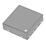
STL11N65M5
N-channel 650 V, 0.475 Ω typ., 8.5 A MDmesh™ M5
Power MOSFET in a PowerFLAT™ 5x5 package
Datasheet - production data
Features
6
7
Order code
VDS @ Tj max.
RDS(on) max
ID
STL11N65M5
710 V
0.530 Ω
8.5 A
5
• Extremely low RDS(on)
10
4
• Low gate charge and input capacitance
11
12
PowerFLAT
TM
1
• Excellent switching performance
5x5
• 100% avalanche tested
Applications
• Switching applications
Description
Figure 1. Internal schematic diagrams
G
10
D(5, 6, 11, 12)
S
9
S
8
S
7
D 11
6D
D 12
5D
G(10)
S(2, 3, 4, 7, 8, 9)
Pin 1
identification
1
NC
2
S
3
S
This device is an N-channel Power MOSFET
based on MDmesh™ M5 innovative vertical
process technology combined with the wellknown PowerMESH™ horizontal layout. The
resulting product offers extremely low onresistance, making it particularly suitable for
applications requiring high power and superior
efficiency.
4
S
Top View
AM15540v5
Table 1. Device summary
Order code
Marking
Package
Packaging
STL11N65M5
11N65M5
PowerFLAT™ 5x5
Tape and reel
October 2014
This is information on a product in full production.
DocID026330 Rev 2
1/14
www.st.com
�Contents
STL11N65M5
Contents
1
Electrical ratings . . . . . . . . . . . . . . . . . . . . . . . . . . . . . . . . . . . . . . . . . . . . 3
2
Electrical characteristics . . . . . . . . . . . . . . . . . . . . . . . . . . . . . . . . . . . . . 4
2.1
Electrical characteristics (curves)
............................ 6
3
Test circuits
4
Package mechanical data . . . . . . . . . . . . . . . . . . . . . . . . . . . . . . . . . . . . 10
5
Revision history . . . . . . . . . . . . . . . . . . . . . . . . . . . . . . . . . . . . . . . . . . . 13
2/14
.............................................. 9
DocID026330 Rev 2
�STL11N65M5
1
Electrical ratings
Electrical ratings
Table 2. Absolute maximum ratings
Symbol
Parameter
Value
Unit
VDS
Drain-source voltage
650
V
VGS
Gate-source voltage
± 25
V
Drain current (continuous) at TC = 25 °C
8.5
A
Drain current (continuous) at TC = 100 °C
4.9
A
Drain current (pulsed)
34
A
ID
(1)
ID (1)
IDM
(1),(2)
ID(3)
Drain current (continuous) at Tpcb=25°C
1.35
A
ID(3)
Drain current (continuous) at Tpcb=100°C
0.86
A
IDM(2),(3) Drain current (pulsed)
5.4
A
PTOT(1)
Total dissipation at TC = 25 °C
70
W
IAR
Avalanche current, repetitive or notrepetitive (pulse width limited by Tj max)
1.9
A
EAS
Single pulse avalanche energy
(starting Tj = 25 °C, ID = IAR, VDD = 50 V)
130
mJ
Peak diode recovery voltage slope
15
V/ns
dv/dt (4)
Tstg
Storage temperature
°C
- 55 to 150
Tj
Max. operating junction temperature
°C
1. Limited by maximum junction temperature
2. Pulse width limited by safe operating area.
3. When mounted on FR-4 Board of 1 inch², 2 oz Cu (t < 100 s)
4. ISD ≤ 8.5 A, di/dt ≤ 400 A/µs, VPeak ≤ V(BR)DSS, VDD = 400 V.
Table 3. Thermal data
Symbol
Rthj-case
Rthj-pcb
(1)
Parameter
Value
Unit
Thermal resistance junction-case max
1.78
°C/W
Thermal resistance junction-pcb max
58.5
°C/W
1. When mounted on 1inch² FR-4 board, 2 oz Cu, t
很抱歉,暂时无法提供与“STL11N65M5”相匹配的价格&库存,您可以联系我们找货
免费人工找货- 国内价格 香港价格
- 1+24.461561+3.14140
- 10+16.2783810+2.09050
- 25+14.6065425+1.87580
- 100+12.40676100+1.59330
- 250+11.96681250+1.53680
