STL33N60M6
Datasheet
N-channel 600 V, 0.115 Ω typ., 21 A MDmesh™ M6 Power MOSFET
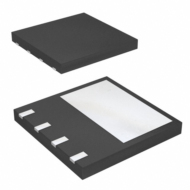
in a PowerFLAT™ 8x8 HV package
Features
5
4
3
2
1
PowerFLAT™ 8x8 HV
Drain(5)
Order code
VDS
RDS(on) max.
ID
STL33N60M6
600 V
137 mΩ
21 A
•
•
Reduced switching losses
Lower RDS(on) per area vs previous generation
•
•
•
Low gate input resistance
100% avalanche tested
Zener-protected
Applications
•
•
•
Gate(1)
Driver
source (2)
Power
source (3, 4)
NG1DS2PS34D5Z
Product status link
Switching applications
LLC converters
Boost PFC converters
Description
The new MDmesh™ M6 technology incorporates the most recent advancements to
the well-known and consolidated MDmesh family of SJ MOSFETs.
STMicroelectronics builds on the previous generation of MDmesh devices through its
new M6 technology, which combines excellent RDS(on) per area improvement with
one of the most effective switching behaviors available, as well as a user-friendly
experience for maximum end-application efficiency.
STL33N60M6
Product summary
Order code
STL33N60M6
Marking
33N60M6
Package
PowerFLAT™ 8x8 HV
Packing
Tape and reel
DS12638 - Rev 3 - August 2018
For further information contact your local STMicroelectronics sales office.
www.st.com
�STL33N60M6
Electrical ratings
1
Electrical ratings
Table 1. Absolute maximum ratings
Symbol
Value
Unit
Gate-source voltage
±25
V
Drain current (continuous) at Tcase = 25 °C
21
Drain current (continuous) at Tcase = 100 °C
13
IDM(1)
Drain current (pulsed)
78
A
PTOT
Total dissipation at Tcase = 25 °C
150
W
dv/dt(2)
Peak diode recovery voltage slope
15
dv/dt(3)
MOSFET dv/dt ruggedness
50
Tstg
Storage temperature range
VGS
ID
Tj
Parameter
A
V/ns
-55 to 150
°C
Value
Unit
Thermal resistance junction-case
0.83
°C/W
Thermal resistance junction-pcb
45
°C/W
Value
Unit
4
A
500
mJ
Operating junction temperature range
1. Pulse width is limited by safe operating area.
2. ISD ≤ 21 A, di/dt = 400 A/μs, VDS < V(BR)DSS, VDD = 400 V
3. VDS ≤ 480 V
Table 2. Thermal data
Symbol
Rthj-case
Rthj-pcb
(1)
Parameter
1. When mounted on FR-4 board of inch², 2oz Cu.
Table 3. Avalanche characteristics
Symbol
IAR
EAS
DS12638 - Rev 3
Parameter
Avalanche current, repetitive or non-repetitive
(pulse width limited by TJmax)
Single pulse avalanche energy
(starting Tj = 25 °C, ID = IAR, VDD = 50 V)
page 2/15
�STL33N60M6
Electrical characteristics
2
Electrical characteristics
(Tcase = 25 °C unless otherwise specified).
Table 4. On/off states
Symbol
V(BR)DSS
Parameter
Drain-source breakdown
voltage
Test conditions
VGS = 0 V, ID = 1 mA
Min.
Typ.
600
Zero gate voltage drain current
IGSS
1
VGS = 0 V, VDS = 600 V,
Tcase = 125
100
°C(1)
Gate-body leakage current
VDS = 0 V, VGS = ±25 V
VGS(th)
Gate threshold voltage
VDS = VGS, ID = 250 µA
RDS(on)
Static drain-source onresistance
VGS = 10 V, ID = 10.5 A
Unit
V
VGS = 0 V, VDS = 600 V
IDSS
Max.
µA
±5
µA
4
4.75
V
0.115
0.137
Ω
Min.
Typ.
Max.
Unit
-
1515
-
-
128
-
-
4.2
-
3.25
1. Defined by design, not subject to production test.
Table 5. Dynamic
Symbol
Parameter
Ciss
Input capacitance
Coss
Output capacitance
Crss
Test conditions
VDS = 100 V, f = 1 MHz, VGS = 0 V
Reverse transfer capacitance
(1)
pF
Equivalent output capacitance
VDS = 0 to 480 V, VGS = 0 V
-
269
-
pF
RG
Intrinsic gate resistance
f = 1 MHz, ID = 0 A
-
1.5
-
Ω
Qg
Total gate charge
VDD = 480 V, ID = 25 A,
-
33.4
-
Qgs
Gate-source charge
VGS = 0 to 10 V
-
7.2
-
Gate-drain charge
(see Figure 14. Test circuit for gate
charge behavior)
-
16.3
-
Coss eq.
Qgd
nC
1. Coss eq. is defined as a constant equivalent capacitance giving the same charging time as Coss when VDS increases from 0
to 80% VDSS.
Table 6. Switching times
Symbol
td(on)
tr
td(off)
tf
DS12638 - Rev 3
Parameter
Test conditions
Min.
Typ.
Max.
Turn-on delay time
VDD = 300 V, ID = 12.5 A,
-
19.5
-
Rise time
RG = 4.7 Ω, VGS = 10 V
-
33
-
Turn-off delay time
(see Figure 13. Switching times test
circuit for resistive load and Figure
18. Switching time waveform)
-
38.5
-
-
7.5
-
Fall time
Unit
ns
page 3/15
�STL33N60M6
Electrical characteristics
Table 7. Source-drain diode
Symbol
ISD
ISDM (1)
(2)
Parameter
Test conditions
Min.
Typ.
Max.
Unit
Source-drain current
-
21
A
Source-drain current (pulsed)
-
78
A
1.6
V
Forward on voltage
ISD = 21 A, VGS = 0 V
-
trr
Reverse recovery time
ISD = 25 A, di/dt = 100 A/µs,
-
265
ns
Qrr
Reverse recovery charge
VDD = 60 V
-
3.07
µC
Reverse recovery current
(see Figure 15. Test circuit for inductive
load switching and diode recovery times)
-
23.2
A
Reverse recovery time
ISD = 25 A, di/dt = 100 A/µs, VDD = 60 V,
-
374
ns
Reverse recovery charge
Tj = 150 °C
-
5.78
µC
Reverse recovery current
(see Figure 15. Test circuit for inductive
load switching and diode recovery times)
-
30.9
A
VSD
IRRM
trr
Qrr
IRRM
1. Pulse width is limited by safe operating area.
2. Pulsed: pulse duration = 300 µs, duty cycle 1.5%
DS12638 - Rev 3
page 4/15
�STL33N60M6
Electrical characteristics (curves)
2.1
Electrical characteristics (curves)
Figure 1. Safe operating area
ID
(A)
Figure 2. Thermal impedance
GIPG200620181213SOA
K
PowerFLAT8x8HVzth
δ =0.5
tp =1 µs
δ =0.2
tp =10 µs
10 1
δ =0.1
tp =100 µs
Operation in this area is
limited by R DS(on)
10 -1
δ =0.01
TJ≤150 °C
TC=25 °C
VGS=10 V
single pulse
10 -1
10 -1
10 0
10 1
VDS (V)
10 2
10 -2
10 -5
70
VGS =8 V
GIPG150620181233TCH
VDS = 20 V
50
VGS =7 V
40
40
30
30
20
20
VGS =6 V
10
10
VGS =5 V
0
0
4
8
12
16
VDS (V)
Figure 5. Gate charge vs gate-source voltage
VGS
(V)
GIPG150620181237QVG VDS
(V)
VDD = 480 V
ID = 25 A
12
600
VDS
400
6
300
4
200
2
100
8
0
3
4
16
24
32
40
0
Qg (nC)
5
6
7
8
9
VGS (V)
Figure 6. Static drain-source on-resistance
RDS(on)
(Ω)
GIPG260620180835RID
0.125
VGS = 10 V
500
8
0
0
t p (s)
10 -2
60
50
10
10 -3
ID
(A)
VGS = 9, 10 V
60
10 -4
Ƭ
Figure 4. Transfer characteristics
GIPG150620181232OCH
70
tp
Single pulse
tp =10 ms
Figure 3. Output characteristics
ID
(A)
Z th =K*R thj-c
δ=t p / Ƭ
δ =0.02
tp =1 ms
10 0
DS12638 - Rev 3
δ =0.05
0.120
0.115
0.110
0.105
0
4
8
12
16
20
ID (A)
page 5/15
�STL33N60M6
Electrical characteristics (curves)
Figure 7. Capacitance variations
C
(pF)
GIPG150620181232CVR
Figure 8. Normalized gate threshold voltage vs
temperature
VGS(th)
(norm.)
10 4
GIPG150620181230VTH
ID = 250 μA
1.1
CISS
10 3
1.0
0.9
10 2
COSS
f = 1 MHz
10 1
10
10 -1
CRSS
0
10 0
10 1
VDS (V)
10 2
Figure 9. Normalized on-resistance vs temperature
RDS(on)
(norm.)
GIPG150620181231RON
VGS = 10 V
2.5
0.8
0.7
0.6
-75
1.00
1.0
0.96
0.5
0.92
75
125
TJ (°C)
Figure 11. Output capacitance stored energy
EOSS
(µJ)
GADG200620181116EOS
14
ID = 1 mA
0.88
-75
-25
25
75
125
TJ (°C)
Figure 12. Source-drain diode forward characteristics
VSD
(V)
GIPG260620180841SDF
Tj = -50 °C
1.0
10
0.9
Tj = 25 °C
8
0.8
6
0.7
4
Tj = 150 °C
0.6
2
DS12638 - Rev 3
TJ (°C)
1.1
12
0
0
125
GIPG150620181231BDV
1.08
1.5
25
75
V(BR)DSS
(norm.)
1.04
-25
25
Figure 10. Normalized V(BR)DSS vs temperature
2.0
0.0
-75
-25
100
200
300
400
500
600
VDS (V)
0.5
0
4
8
12
16
20
ISD (A)
page 6/15
�STL33N60M6
Test circuits
3
Test circuits
Figure 13. Switching times test circuit for resistive load
Figure 14. Test circuit for gate charge behavior
VDD
RL
RL
+
VD
VGS
3.3
µF
2200
µF
VDD
IG= CONST
VGS
RG
+
pulse width
D.U.T.
2200
μF
PW
D.U.T.
100 Ω
2.7 kΩ
VG
47 kΩ
GND1
(driver signal)
GND2
(power)
1 kΩ
GND1
AM15855v1
GND2
GADG180720181011SA
Figure 15. Test circuit for inductive load switching and
diode recovery times
A
A
D.U.T.
FAST
DIODE
Figure 16. Unclamped inductive load test circuit
A
L
D
G
S
L=100µH
B
B
D
25Ω
VD
3.3
µF
B
+
1000
µF
2200
µF
3.3
µF
+
VDD
VDD
ID
G
S
RG
D.U.T.
Vi
D.U.T.
Pw
GND2
GND1
GND1
GND2
AM15858v1
AM15857v1
Figure 18. Switching time waveform
Figure 17. Unclamped inductive waveform
ton
V(BR)DSS
td(on)
VD
toff
td(off)
tr
tf
90%
90%
IDM
VDD
10%
0
ID
VDD
AM01472v1
VGS
0
VDS
10%
90%
10%
AM01473v1
DS12638 - Rev 3
page 7/15
�STL33N60M6
Package information
4
Package information
In order to meet environmental requirements, ST offers these devices in different grades of ECOPACK®
packages, depending on their level of environmental compliance. ECOPACK® specifications, grade definitions
and product status are available at: www.st.com. ECOPACK® is an ST trademark.
DS12638 - Rev 3
page 8/15
�STL33N60M6
PowerFLAT™ 8x8 HV package information
4.1
PowerFLAT™ 8x8 HV package information
Figure 19. PowerFLAT™ 8x8 HV package outline
8222871_Rev_4
DS12638 - Rev 3
page 9/15
�STL33N60M6
PowerFLAT™ 8x8 HV package information
Table 8. PowerFLAT™ 8x8 HV mechanical data
Ref.
Dimensions (in mm)
Min.
Typ.
Max.
A
0.75
0.85
0.95
A1
0.00
A3
0.10
0.20
0.30
b
0.90
1.00
1.10
D
7.90
8.00
8.10
E
7.90
8.00
8.10
D2
7.10
7.20
7.30
E1
2.65
2.75
2.85
E2
4.25
4.35
4.45
e
L
0.05
2.00 BSC
0.40
0.50
0.60
Figure 20. PowerFLAT™ 8x8 HV footprint
8222871_REV_4_footprint
Note:
DS12638 - Rev 3
All dimensions are in millimeters.
page 10/15
�STL33N60M6
PowerFLAT™ 8x8 HV packing information
4.2
PowerFLAT™ 8x8 HV packing information
Figure 21. PowerFLAT™ 8x8 HV tape
P2 (2.0±0.1)
T (0.30±0.05)
P0 (4.0±0.1)
D0 ( 1.55±0.05)
D1 ( 1.5 Min)
P1 (12.00±0.1)
W (16.00±0.3)
F (7.50±0.1)
B0 (8.30±0.1)
E (1.75±0.1)
A0 (8.30±0.1)
K0 (1.10±0.1)
Note: Base and Bulk qu antity 3000 pcs
8229819_Tape_revA
Note:
All dimensions are in millimeters.
Figure 22. PowerFLAT™ 8x8 HV package orientation in carrier tape
DS12638 - Rev 3
page 11/15
�STL33N60M6
PowerFLAT™ 8x8 HV packing information
Figure 23. PowerFLAT™ 8x8 HV reel
8229819_Reel_revA
Note:
DS12638 - Rev 3
All dimensions are in millimeters.
page 12/15
�STL33N60M6
Revision history
Table 9. Document revision history
DS12638 - Rev 3
Date
Version
02-Jul-2018
1
18-Jul-2018
2
02-Aug-2018
3
Changes
Initial release.
Modified Section 3 Test circuits.
Minor text changes.
Updated features in cover page.
page 13/15
�STL33N60M6
Contents
Contents
1
Electrical ratings . . . . . . . . . . . . . . . . . . . . . . . . . . . . . . . . . . . . . . . . . . . . . . . . . . . . . . . . . . . . . . . . . .2
2
Electrical characteristics. . . . . . . . . . . . . . . . . . . . . . . . . . . . . . . . . . . . . . . . . . . . . . . . . . . . . . . . . . . 3
2.1
Electrical characteristics (curves) . . . . . . . . . . . . . . . . . . . . . . . . . . . . . . . . . . . . . . . . . . . . . . . . . 5
3
Test circuits . . . . . . . . . . . . . . . . . . . . . . . . . . . . . . . . . . . . . . . . . . . . . . . . . . . . . . . . . . . . . . . . . . . . . . .7
4
Package information. . . . . . . . . . . . . . . . . . . . . . . . . . . . . . . . . . . . . . . . . . . . . . . . . . . . . . . . . . . . . . .8
4.1
PowerFLAT™ 8x8 HV package information. . . . . . . . . . . . . . . . . . . . . . . . . . . . . . . . . . . . . . . . . 8
4.2
PowerFLAT™ 8x8 HV packing information . . . . . . . . . . . . . . . . . . . . . . . . . . . . . . . . . . . . . . . . 10
Revision history . . . . . . . . . . . . . . . . . . . . . . . . . . . . . . . . . . . . . . . . . . . . . . . . . . . . . . . . . . . . . . . . . . . . . . .13
DS12638 - Rev 3
page 14/15
�STL33N60M6
IMPORTANT NOTICE – PLEASE READ CAREFULLY
STMicroelectronics NV and its subsidiaries (“ST”) reserve the right to make changes, corrections, enhancements, modifications, and improvements to ST
products and/or to this document at any time without notice. Purchasers should obtain the latest relevant information on ST products before placing orders. ST
products are sold pursuant to ST’s terms and conditions of sale in place at the time of order acknowledgement.
Purchasers are solely responsible for the choice, selection, and use of ST products and ST assumes no liability for application assistance or the design of
Purchasers’ products.
No license, express or implied, to any intellectual property right is granted by ST herein.
Resale of ST products with provisions different from the information set forth herein shall void any warranty granted by ST for such product.
ST and the ST logo are trademarks of ST. All other product or service names are the property of their respective owners.
Information in this document supersedes and replaces information previously supplied in any prior versions of this document.
© 2018 STMicroelectronics – All rights reserved
DS12638 - Rev 3
page 15/15
�


 工商网监
湘ICP备2023018690号
工商网监
湘ICP备2023018690号
