STL60N32N3LL
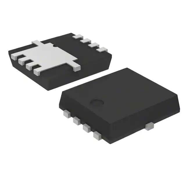
Dual N-channel 30 V, 0.005 Ω, 15 A PowerFLAT™ 5x6
asymmetrical double island, STripFET™ Power MOSFET
Features
Order code
STL60N32N3LL
■
VDSS
Q1
Q2
RDS(on)
ID
30 V
< 0.0092 Ω 13.6 A
30 V
< 0.0055 Ω 15 A
4
3
2
1
S1/D2
RDS(on) * Qg industry benchmark
■
Extremely low on-resistance RDS(on)
■
Very low switching gate charge
■
High avalanche ruggedness
■
Low gate drive power losses
S2
D1
5
G1
6
7
8
G2
PowerFLAT™5x6 asymmetrical
double island
Application
■
Switching applications
Figure 1.
Description
Internal schematic diagram
$�
�
� 3�
$�
�
� 3�
$�
�
'�
�
� 3�
This device is a dual N-channel Power MOSFET
which utilizes the latest generation of design rules
for ST's proprietary STripFET™ V and
STripFET™ VI DeepGATE™ technology. The
lowest available RDS(on)* Qg in this chip scale
package renders the device suitable for the most
demanding DC-DC converter applications, where
high power density is required.
� '�
1�
1�
(top view)
Table 1.
!-�����V�
Device summary
Order code
Marking
Package
Packaging
STL60N32N3LL
60N32N3LL
PowerFLAT™5x6
asymmetrical double island
Tape and reel
February 2012
Doc ID 17266 Rev 3
1/14
www.st.com
14
�Contents
STL60N32N3LL
Contents
1
Electrical ratings . . . . . . . . . . . . . . . . . . . . . . . . . . . . . . . . . . . . . . . . . . . . 3
2
Electrical characteristics . . . . . . . . . . . . . . . . . . . . . . . . . . . . . . . . . . . . . 4
2.1
Electrical characteristics (curves) . . . . . . . . . . . . . . . . . . . . . . . . . . . . . . . . 6
2.1.1
Graphs for Q1
..........................................6
2.1.2
Graphs for Q2
..........................................8
3
Test circuits
4
Package mechanical data . . . . . . . . . . . . . . . . . . . . . . . . . . . . . . . . . . . . 11
5
Revision history . . . . . . . . . . . . . . . . . . . . . . . . . . . . . . . . . . . . . . . . . . . 13
2/14
. . . . . . . . . . . . . . . . . . . . . . . . . . . . . . . . . . . . . . . . . . . . . 10
Doc ID 17266 Rev 3
�STL60N32N3LL
1
Electrical ratings
Electrical ratings
Table 2.
Symbol
Absolute maximum ratings
Parameter
Type
Value
Unit
VDS
Drain-source voltage
Q1
Q2
30
30
V
V
VGS
Gate- source voltage
Q1
Q2
± 20
± 20
V
V
ID(1)
Drain current (continuous) at TC = 25 °C
Q1
Q2
32
60
A
A
ID(1)
Drain current (continuous) at
TC = 100 °C
Q1
Q2
23
37
A
A
ID(2)
Drain current (continuous) at
Tpcb = 25 °C
Q1
Q2
13.6
15
A
A
ID(2)
Drain current (continuous) at
Tpcb = 100 °C
Q1
Q2
8.5
9.3
A
A
Drain current (pulsed)
Q1
Q2
54.4
60
A
A
PTOT(1)
Total dissipation at TC = 25 °C
Q1
Q2
23
50
W
W
PTOT(2)
Total dissipation at Tpcb = 25 °C
Q1
Q2
3.12
3.12
W
W
Tj
Operating junction temperature
-55 to 150
°C
Value
Unit
40
°C/W
5.5
2.5
°C/W
IDM (2),(3)
Tstg
Storage temperature
1. This value is according toRthj-c
2. This value is according toRthj-pcb
3. Pulse width limited by safe operating area
Table 3.
Symbol
Rthj-pcb(1)
Rthj-c
Thermal data
Parameter
Type
Thermal resistance junction-pcb max
Thermal resistance junction-case
Q1
Q2
1. When mounted on FR-4 board of 1inch², 2oz Cu, t < 10 sec
Doc ID 17266 Rev 3
3/14
�Electrical characteristics
2
STL60N32N3LL
Electrical characteristics
(TCASE=25°C unless otherwise specified)
Table 4.
Symbol
Parameter
Test conditions
Type
Min.
30
30
Typ.
Max.
Unit
Drain-source
Breakdown voltage
ID = 250 µA, VGS = 0
Q1
Q2
IDSS
Zero gate voltage
Drain current (VGS = 0)
VDS = 30 V
Q1
Q2
1
1
µA
µA
IDSS
Zero gate voltage
Drain current (VGS = 0)
VDS =30 V, TC =125°C
Q1
Q2
10
10
µA
µA
IGSS
Gate-body leakage
current (VDS = 0)
VGS = ± 20 V
Q1
Q2
±100
±100
nA
nA
VGS(th)
Gate threshold voltage
VDS = VGS,
ID = 250 µA
Q1
Q2
RDS(on)
Static drain-source on
resistance
VGS = 10 V, ID = 6.8 A
VGS = 10 V, ID = 7.5 A
Q1
Q2
0.0085 0.0092
0.005 0.0055
Ω
Ω
RDS(on)
Static drain-source on
resistance
VGS = 4.5 V, ID = 6.8 A
VGS = 4.5 V, ID = 7.5 A
Q1
Q2
0.0109 0.012
0.0065 0.0073
Ω
Ω
Test conditions
Type
Min.
Typ.
Max.
Unit
Q1
Q2
-
950
1690
-
pF
pF
Q1
Q2
-
193
291
-
pF
pF
V(BR)DSS
Table 5.
Symbol
4/14
On/off states
V
V
1
1
V
V
Dynamic
Parameter
Ciss
Input capacitance
Coss
Output capacitance
Crss
Reverse transfer
capacitance
Q1
Q2
-
27.6
176
-
pF
pF
Qg
Total gate charge
Q1
Q2
-
6.6
17
-
nC
nC
Qgs
Gate-source charge
Q1
Q2
-
3.3
8
-
nC
nC
Qgd
Gate-drain charge
Q1
Q2
-
2.4
6
-
nC
nC
VDS = 25 V, f = 1 MHz,
VGS = 0
VDD = 15 V, ID = 15 A,
VGS = 4.5 V
(see Figure 25)
Doc ID 17266 Rev 3
�STL60N32N3LL
Electrical characteristics
Table 6.
Symbol
Switching times
Parameter
Test conditions
Type
Turn-on delay time
Rise time
VDD=15 V, ID=7.5 A,
RG=4.7 Ω,
VGS= 4.5 V
(see Figure 29)
Q1
Q2
Q1
Q2
Turn-off delay time
Fall time
VDD=15 V, ID=7.5 A,
RG=4.7 Ω,
VGS= 4.5V
(see Figure 29)
td(on)
tr
td(off)
tf
Table 7.
Symbol
Min.
Typ.
Max.
Unit
-
10.8
9.5
15.6
30
-
ns
ns
ns
ns
Q1
Q2
Q1
Q2
-
14.2
37
6
12
-
ns
ns
ns
ns
Test conditions
Type
Min.
Typ.
Max.
Unit
Q1
Q2
-
13.6
15
A
A
Source drain diode
Parameter
ISD
Source-drain current
VDD=15 V, ID=7.5 A
RG=4.7 Ω,
VGS=4.5 V
ISDM (1)
Source-drain current
(pulsed)
VDD=15 V, ID= 7.5 A
RG=4.7 Ω,
VGS=4.5 V
Q1
Q2
-
54.4
60
A
A
VSD (2)
Forward on voltage
ISD = 15 A, VGS = 0
Q1
Q2
-
1.1
1.1
V
V
trr
Qrr
IRRM
Reverse recovery time
ISD = 15 A,
VDD = 15 V
Reverse recovery charge
di/dt = 100 A/µs,
T = 150°C
Reverse recovery current j
(see Figure 29)
Q1
Q2
Q1
Q2
Q1
Q2
-
20
24
10
16.8
1
1.4
ns
ns
nC
nC
A
A
1. Pulse width limited by safe operating area.
2. Pulsed: Pulse duration = 300 µs, duty cycle 1.5%
Doc ID 17266 Rev 3
5/14
�Electrical characteristics
STL60N32N3LL
2.1
Electrical characteristics (curves)
2.1.1
Graphs for Q1
Figure 2.
Safe operating area
Figure 3.
Thermal impedance
AM11199v1
ID
(A)
PCB_PowerFLAT
K
Tj=150°C
Tc=25°C
Single pulse
100
a is
are n)
S(o
this
in x RD
a
on
rati by m
e
Op ited
Lim
0
10
δ=0.5
0.2
100ms
10
0.1
-1
10
0.05
10ms
1
0.02
-2
10
1s
0.01
-3
0.1
10
Single pulse
-4
0.01
0.1
Figure 4.
10
1
VDS(V)
Output characteristics
10 -3
10
Figure 5.
AM11200v1
ID
(A)
-2
0
-1
10
2
1
10
10
tp (s)
10
10
Transfer characteristics
AM11201v1
ID
(A)
4V
50
50
40
40
30
30
20
20
VDS=3V
3V
10
0
0
Figure 6.
1
2
3
4
0
0
VDS(V)
Normalized BVDSS vs temperature
AM11202v1
BVDSS
10
(norm)
Figure 7.
1
2
4
3
VGS(V)
Static drain-source on resistance
AM11203v1
RDS(on)
(mΩ)
1.12
VGS=10V
ID=1mA
12.5
1.08
10.5
1.04
8.5
1.00
6.5
0.96
0.92
-25
6/14
25
75
125
TJ(°C)
4.5
2
Doc ID 17266 Rev 3
4
6
8
10
12
ID(A)
�STL60N32N3LL
Figure 8.
Electrical characteristics
Gate charge vs gate-source voltage Figure 9.
AM11204v1
VGS
(V)
VDD=15V
ID=13.6A
10
Capacitance variations
AM11205v1
C
(pF)
1410
1210
8
1010
Ciss
810
6
610
4
410
2
210
0
0
4
2
6
8
10
12
14
Qg(nC)
Figure 10. Normalized gate threshold voltage
vs temperature
AM11206v1
VGS(th)
(norm)
Coss
10
0
10
Crss
VDS(V)
20
Figure 11. Normalized on resistance vs
temperature
AM11207v1
RDS(on)
(norm)
ID=250µA
1.8
1.2
1.6
1.0
1.4
0.8
1.2
0.6
1.0
0.4
0.8
0.2
0.6
0.4
0
25
-25
75
125
TJ(°C)
-25
25
75
125
TJ(°C)
Figure 12. Source-drain diode forward
characteristics
AM11208v1
VSD
(V)
TJ=-55°C
0.9
TJ=25°C
0.8
0.7
TJ=175°C
0.6
0.5
0.4
2
4
6
8
10
12 ISD(A)
Doc ID 17266 Rev 3
7/14
�Electrical characteristics
2.1.2
STL60N32N3LL
Graphs for Q2
Figure 13. Safe operating area
Figure 14. Thermal impedance
AM11209v1
ID
(A)
100
PCB_PowerFLAT
K
Tj=150°C
Tc=25°C
Single pulse
a is
are n)
S(o
this
in x RD
a
on
rati by m
e
Op ited
Lim
0
10
δ=0.5
0.2
100ms
10
0.1
-1
10
0.05
10ms
1
0.02
-2
10
1s
0.01
-3
0.1
10
Single pulse
-4
0.01
0.1
10
1
VDS(V)
Figure 15. Output characteristics
10 -3
10
-2
0
-1
10
10
10
tp (s)
Figure 16. Transfer characteristics
AM11210v1
ID
(A)
60
AM11211v1
ID
(A)
60
4V
50
50
40
40
3V
30
20
10
10
1
2
4
3
5
AM11212v1
BVDSS
0
0
VDS(V)
Figure 17. Normalized BVDSS vs temperature
(norm)
VDS=3V
30
20
0
0
2
1
10
10
1
2
4
3
VGS(V)
Figure 18. Static drain-source on resistance
AM11213v1
RDS(on)
(mΩ)
VGS=10V
ID=1mA
1.04
8
1.00
6
0.96
4
0.92
-25
8/14
25
75
125
TJ(°C)
Doc ID 17266 Rev 3
2
0
2
4
6
8
10
ID(A)
�STL60N32N3LL
Electrical characteristics
Figure 19. Gate charge vs gate-source voltage Figure 20. Capacitance variations
AM11214v1
VGS
(V)
VDD=15V
ID=15A
12
AM11215v1
C
(pF)
1600
10
Ciss
1100
8
6
600
4
100
2
Coss
Crss
0
0
10
5
15
20
30
25
35
Figure 21. Normalized gate threshold voltage
vs temperature
AM11216v1
VGS(th)
(norm)
10
VDS(V)
20
Figure 22. Normalized on resistance vs
temperature
AM11217v1
RDS(on)
(norm)
ID=250µA
1.2
0
Qg(nC)
1.6
1.1
1.4
1.0
0.9
1.2
0.8
1.0
0.7
0.8
0.6
0.6
0.5
0.4
25
-25
75
TJ(°C)
125
0.4
-75
-25
25
75
125
175 TJ(°C)
Figure 23. Source-drain diode forward
characteristics
AM11218v1
VSD
(V)
0.9
TJ=-55°C
0.8
TJ=25°C
0.7
0.6
TJ=175°C
0.5
0.4
0
2
4
6
8
10
ISD(A)
Doc ID 17266 Rev 3
9/14
�Test circuits
3
STL60N32N3LL
Test circuits
Figure 24. Switching times test circuit for
resistive load
Figure 25. Gate charge test circuit
VDD
12V
47kΩ
1kΩ
100nF
3.3
μF
2200
RL
μF
VGS
IG=CONST
VDD
100Ω
Vi=20V=VGMAX
VD
RG
2200
μF
D.U.T.
D.U.T.
VG
2.7kΩ
PW
47kΩ
1kΩ
PW
AM01468v1
AM01469v1
Figure 26. Test circuit for inductive load
Figure 27. Unclamped inductive load test
switching and diode recovery times
circuit
A
A
D.U.T.
FAST
DIODE
B
B
L
A
D
G
VD
L=100μH
S
3.3
μF
B
25 Ω
1000
μF
D
VDD
2200
μF
3.3
μF
VDD
ID
G
RG
S
Vi
D.U.T.
Pw
AM01470v1
Figure 28. Unclamped inductive waveform
AM01471v1
Figure 29. Switching time waveform
ton
V(BR)DSS
tdon
VD
toff
tr
tdoff
tf
90%
90%
IDM
10%
ID
VDD
10%
0
VDD
VDS
90%
VGS
AM01472v1
10/14
0
Doc ID 17266 Rev 3
10%
AM01473v1
�STL60N32N3LL
4
Package mechanical data
Package mechanical data
In order to meet environmental requirements, ST offers these devices in different grades of
ECOPACK® packages, depending on their level of environmental compliance. ECOPACK®
specifications, grade definitions and product status are available at: www.st.com. ECOPACK
is an ST trademark.
Table 8.
PowerFLAT™ 5x6 asymmetrical double island dimentions
mm
Dim.
Min.
A
Typ.
0.80
Max.
1.00
A1
0.05
b
0.45
0.55
D
4.90
5.00
5.10
E
5.90
6.00
6.10
e
L
1.27
0.40
0.60
aaa
0.10
bbb
0.10
ccc
0.10
Doc ID 17266 Rev 3
11/14
�Package mechanical data
STL60N32N3LL
Figure 30. Package drawing
8202594_Rev_B
Figure 31. Recommended footprint (dimensions are in mm)
footprint
12/14
Doc ID 17266 Rev 3
�STL60N32N3LL
5
Revision history
Revision history
Table 9.
Document revision history
Date
Revision
15-Mar-2010
1
First release
07-Feb-2011
2
Document status promoted from target specification to preliminary
data.
3
Document status promoted from preliminary data to datasheet.
Section 2.1: Electrical characteristics (curves) has been added.
Section 4: Package mechanical data has been updated.
Minor text changes.
21-Feb-2012
Changes
Doc ID 17266 Rev 3
13/14
�STL60N32N3LL
Please Read Carefully:
Information in this document is provided solely in connection with ST products. STMicroelectronics NV and its subsidiaries (“ST”) reserve the
right to make changes, corrections, modifications or improvements, to this document, and the products and services described herein at any
time, without notice.
All ST products are sold pursuant to ST’s terms and conditions of sale.
Purchasers are solely responsible for the choice, selection and use of the ST products and services described herein, and ST assumes no
liability whatsoever relating to the choice, selection or use of the ST products and services described herein.
No license, express or implied, by estoppel or otherwise, to any intellectual property rights is granted under this document. If any part of this
document refers to any third party products or services it shall not be deemed a license grant by ST for the use of such third party products
or services, or any intellectual property contained therein or considered as a warranty covering the use in any manner whatsoever of such
third party products or services or any intellectual property contained therein.
UNLESS OTHERWISE SET FORTH IN ST’S TERMS AND CONDITIONS OF SALE ST DISCLAIMS ANY EXPRESS OR IMPLIED
WARRANTY WITH RESPECT TO THE USE AND/OR SALE OF ST PRODUCTS INCLUDING WITHOUT LIMITATION IMPLIED
WARRANTIES OF MERCHANTABILITY, FITNESS FOR A PARTICULAR PURPOSE (AND THEIR EQUIVALENTS UNDER THE LAWS
OF ANY JURISDICTION), OR INFRINGEMENT OF ANY PATENT, COPYRIGHT OR OTHER INTELLECTUAL PROPERTY RIGHT.
UNLESS EXPRESSLY APPROVED IN WRITING BY TWO AUTHORIZED ST REPRESENTATIVES, ST PRODUCTS ARE NOT
RECOMMENDED, AUTHORIZED OR WARRANTED FOR USE IN MILITARY, AIR CRAFT, SPACE, LIFE SAVING, OR LIFE SUSTAINING
APPLICATIONS, NOR IN PRODUCTS OR SYSTEMS WHERE FAILURE OR MALFUNCTION MAY RESULT IN PERSONAL INJURY,
DEATH, OR SEVERE PROPERTY OR ENVIRONMENTAL DAMAGE. ST PRODUCTS WHICH ARE NOT SPECIFIED AS "AUTOMOTIVE
GRADE" MAY ONLY BE USED IN AUTOMOTIVE APPLICATIONS AT USER’S OWN RISK.
Resale of ST products with provisions different from the statements and/or technical features set forth in this document shall immediately void
any warranty granted by ST for the ST product or service described herein and shall not create or extend in any manner whatsoever, any
liability of ST.
ST and the ST logo are trademarks or registered trademarks of ST in various countries.
Information in this document supersedes and replaces all information previously supplied.
The ST logo is a registered trademark of STMicroelectronics. All other names are the property of their respective owners.
© 2012 STMicroelectronics - All rights reserved
STMicroelectronics group of companies
Australia - Belgium - Brazil - Canada - China - Czech Republic - Finland - France - Germany - Hong Kong - India - Israel - Italy - Japan Malaysia - Malta - Morocco - Philippines - Singapore - Spain - Sweden - Switzerland - United Kingdom - United States of America
www.st.com
14/14
Doc ID 17266 Rev 3
�