UM1537
User manual
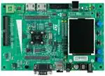
STM320518-EVAL evaluation board
Introduction
The STM320518-EVAL evaluation board is designed as a complete demonstration and
development platform for STMicroelectronic's ARM cortex-M0 core-based
STM32F051R8T6 microcontroller. It features two I2Cs, two SPIs, two USARTs, a 12-bit
ADC, a 12-bit DAC, two GP comparators, internal 8 KB SRAM and 64 KB Flash, touch
sensing, CEC and SWD debugging support.
The full range of hardware features on the board is able to help you evaluate all peripherals
(motor control connector, RS-232, RS-485, audio DAC, linear sensor, microphone ADC,
TFT LCD, IrDA, IR LED, IR receiver, LDR, MicroSD card, CEC on two HDMI connectors, RF
E2PROM, temperature sensor and so on) and develop your own applications. Extension
headers make it possible to easily connect a daughterboard or wrapping board for your
specific application.
An ST-LINK/V2 is integrated on the board as an embedded in-circuit debugger and
programmer for the STM32 MCU.
May 2012
Figure 1.
STM320518-EVAL evaluation board
Table 1.
Applicable tools
Type
Part number
Evaluation tools
STM320518-EVAL
Doc ID 023059 Rev 1
1/52
www.st.com
�Contents
UM1537
Contents
1
2
3
2/52
Overview . . . . . . . . . . . . . . . . . . . . . . . . . . . . . . . . . . . . . . . . . . . . . . . . . . 6
1.1
Features . . . . . . . . . . . . . . . . . . . . . . . . . . . . . . . . . . . . . . . . . . . . . . . . . . . 6
1.2
Demonstration software . . . . . . . . . . . . . . . . . . . . . . . . . . . . . . . . . . . . . . . 6
1.3
Order code . . . . . . . . . . . . . . . . . . . . . . . . . . . . . . . . . . . . . . . . . . . . . . . . . 6
1.4
Delivery recommendations . . . . . . . . . . . . . . . . . . . . . . . . . . . . . . . . . . . . . 7
Hardware layout and configuration . . . . . . . . . . . . . . . . . . . . . . . . . . . . . 8
2.1
Development and debug support . . . . . . . . . . . . . . . . . . . . . . . . . . . . . . . 10
2.2
Power supply . . . . . . . . . . . . . . . . . . . . . . . . . . . . . . . . . . . . . . . . . . . . . . 11
2.3
Clock source . . . . . . . . . . . . . . . . . . . . . . . . . . . . . . . . . . . . . . . . . . . . . . . 13
2.4
Reset source . . . . . . . . . . . . . . . . . . . . . . . . . . . . . . . . . . . . . . . . . . . . . . 13
2.5
Boot option . . . . . . . . . . . . . . . . . . . . . . . . . . . . . . . . . . . . . . . . . . . . . . . . 14
2.6
Audio . . . . . . . . . . . . . . . . . . . . . . . . . . . . . . . . . . . . . . . . . . . . . . . . . . . . 14
2.7
RS-232, RS-485 and IrDA . . . . . . . . . . . . . . . . . . . . . . . . . . . . . . . . . . . . 15
2.8
Linear sensor . . . . . . . . . . . . . . . . . . . . . . . . . . . . . . . . . . . . . . . . . . . . . . 16
2.9
MicroSD card . . . . . . . . . . . . . . . . . . . . . . . . . . . . . . . . . . . . . . . . . . . . . . 16
2.10
Analog input . . . . . . . . . . . . . . . . . . . . . . . . . . . . . . . . . . . . . . . . . . . . . . . 16
2.11
LDR (light dependent resistor) . . . . . . . . . . . . . . . . . . . . . . . . . . . . . . . . . 16
2.12
Temperature sensor . . . . . . . . . . . . . . . . . . . . . . . . . . . . . . . . . . . . . . . . . 17
2.13
Display and input devices . . . . . . . . . . . . . . . . . . . . . . . . . . . . . . . . . . . . . 17
2.14
RF E2PROM . . . . . . . . . . . . . . . . . . . . . . . . . . . . . . . . . . . . . . . . . . . . . . 18
2.15
HDMI CEC . . . . . . . . . . . . . . . . . . . . . . . . . . . . . . . . . . . . . . . . . . . . . . . . 18
2.16
IR LED and IR receiver . . . . . . . . . . . . . . . . . . . . . . . . . . . . . . . . . . . . . . 19
2.17
Motor control . . . . . . . . . . . . . . . . . . . . . . . . . . . . . . . . . . . . . . . . . . . . . . 19
Connector . . . . . . . . . . . . . . . . . . . . . . . . . . . . . . . . . . . . . . . . . . . . . . . . 22
3.1
Motor control connector CN1 . . . . . . . . . . . . . . . . . . . . . . . . . . . . . . . . . . 22
3.2
RF E2PROM connector CN2 . . . . . . . . . . . . . . . . . . . . . . . . . . . . . . . . . . 23
3.3
HDMI sink connector CN3 . . . . . . . . . . . . . . . . . . . . . . . . . . . . . . . . . . . . 23
3.4
HDMI source connector CN4 . . . . . . . . . . . . . . . . . . . . . . . . . . . . . . . . . . 24
3.5
Daughterboard extension connector CN5 and CN6 . . . . . . . . . . . . . . . . . 24
Doc ID 023059 Rev 1
�UM1537
4
Contents
3.6
RS-232 and RS-485 connector CN7 . . . . . . . . . . . . . . . . . . . . . . . . . . . . 27
3.7
Analog input connector CN8 . . . . . . . . . . . . . . . . . . . . . . . . . . . . . . . . . . 28
3.8
High density SWD connector CN9 . . . . . . . . . . . . . . . . . . . . . . . . . . . . . . 28
3.9
Standard SWD connector CN10 . . . . . . . . . . . . . . . . . . . . . . . . . . . . . . . 29
3.10
Audio jack CN11 . . . . . . . . . . . . . . . . . . . . . . . . . . . . . . . . . . . . . . . . . . . . 29
3.11
ST-LINK/V2 programming connector CN12 . . . . . . . . . . . . . . . . . . . . . . . 29
3.12
ST-LINK/V2 USB type B connector CN13 . . . . . . . . . . . . . . . . . . . . . . . . 29
3.13
MicroSD connector CN14 . . . . . . . . . . . . . . . . . . . . . . . . . . . . . . . . . . . . . 30
3.14
Power connector CN15 . . . . . . . . . . . . . . . . . . . . . . . . . . . . . . . . . . . . . . 31
Board schematics . . . . . . . . . . . . . . . . . . . . . . . . . . . . . . . . . . . . . . . . . . 32
Appendix A STM320518-EVAL I/O assignments . . . . . . . . . . . . . . . . . . . . . . . . . 47
Appendix B Mechanical dimensions. . . . . . . . . . . . . . . . . . . . . . . . . . . . . . . . . . . 50
Revision history . . . . . . . . . . . . . . . . . . . . . . . . . . . . . . . . . . . . . . . . . . . . . . . . . . . . 51
Doc ID 023059 Rev 1
3/52
�List of tables
UM1537
List of tables
Table 1.
Table 2.
Table 3.
Table 4.
Table 5.
Table 6.
Table 7.
Table 8.
Table 9.
Table 10.
Table 11.
Table 12.
Table 13.
Table 14.
Table 15.
Table 16.
Table 17.
Table 18.
Table 19.
Table 20.
Table 21.
Table 22.
Table 23.
Table 24.
Table 25.
Table 26.
Table 27.
Table 28.
4/52
Applicable tools. . . . . . . . . . . . . . . . . . . . . . . . . . . . . . . . . . . . . . . . . . . . . . . . . . . . . . . . . . . 1
Third-party toolchain support . . . . . . . . . . . . . . . . . . . . . . . . . . . . . . . . . . . . . . . . . . . . . . . 10
Power source related jumpers . . . . . . . . . . . . . . . . . . . . . . . . . . . . . . . . . . . . . . . . . . . . . . 11
Power mode related jumpers . . . . . . . . . . . . . . . . . . . . . . . . . . . . . . . . . . . . . . . . . . . . . . . 12
8 MHz crystal X1 related solder bridges . . . . . . . . . . . . . . . . . . . . . . . . . . . . . . . . . . . . . . . 13
32 kHz crystal X2 related solder bridges . . . . . . . . . . . . . . . . . . . . . . . . . . . . . . . . . . . . . . 13
Boot related switch . . . . . . . . . . . . . . . . . . . . . . . . . . . . . . . . . . . . . . . . . . . . . . . . . . . . . . . 14
Boot0 related jumpers. . . . . . . . . . . . . . . . . . . . . . . . . . . . . . . . . . . . . . . . . . . . . . . . . . . . . 14
Audio related jumpers . . . . . . . . . . . . . . . . . . . . . . . . . . . . . . . . . . . . . . . . . . . . . . . . . . . . . 14
RS-232 and IrDA related jumpers. . . . . . . . . . . . . . . . . . . . . . . . . . . . . . . . . . . . . . . . . . . . 15
RS-485 related solder bridges . . . . . . . . . . . . . . . . . . . . . . . . . . . . . . . . . . . . . . . . . . . . . . 16
LCD modules . . . . . . . . . . . . . . . . . . . . . . . . . . . . . . . . . . . . . . . . . . . . . . . . . . . . . . . . . . . 17
Motor control related jumpers . . . . . . . . . . . . . . . . . . . . . . . . . . . . . . . . . . . . . . . . . . . . . . . 21
Motor control connector CN1 . . . . . . . . . . . . . . . . . . . . . . . . . . . . . . . . . . . . . . . . . . . . . . . 22
RF E2PROM connector CN2 . . . . . . . . . . . . . . . . . . . . . . . . . . . . . . . . . . . . . . . . . . . . . . . 23
HDMI sink connector CN3 . . . . . . . . . . . . . . . . . . . . . . . . . . . . . . . . . . . . . . . . . . . . . . . . . 24
HDMI source connector CN4 . . . . . . . . . . . . . . . . . . . . . . . . . . . . . . . . . . . . . . . . . . . . . . . 24
Daughterboard extension connector CN5 . . . . . . . . . . . . . . . . . . . . . . . . . . . . . . . . . . . . . 25
Daughterboard extension connector CN6 . . . . . . . . . . . . . . . . . . . . . . . . . . . . . . . . . . . . . 26
RS-232 and RS-485 connector CN7 . . . . . . . . . . . . . . . . . . . . . . . . . . . . . . . . . . . . . . . . . 27
Analog input-output connector CN8 . . . . . . . . . . . . . . . . . . . . . . . . . . . . . . . . . . . . . . . . . . 28
High density SWD debugging connector CN9 . . . . . . . . . . . . . . . . . . . . . . . . . . . . . . . . . . 28
Standard SWD debugging connector CN10 . . . . . . . . . . . . . . . . . . . . . . . . . . . . . . . . . . . . 29
USB type B connector CN13 . . . . . . . . . . . . . . . . . . . . . . . . . . . . . . . . . . . . . . . . . . . . . . . 30
MicroSD connector CN14 . . . . . . . . . . . . . . . . . . . . . . . . . . . . . . . . . . . . . . . . . . . . . . . . . . 30
STM32F051R8T6 MCU pin assignments . . . . . . . . . . . . . . . . . . . . . . . . . . . . . . . . . . . . . . 47
Mechanical dimensions . . . . . . . . . . . . . . . . . . . . . . . . . . . . . . . . . . . . . . . . . . . . . . . . . . . 50
Document revision history . . . . . . . . . . . . . . . . . . . . . . . . . . . . . . . . . . . . . . . . . . . . . . . . . 51
Doc ID 023059 Rev 1
�UM1537
List of figures
List of figures
Figure 1.
Figure 2.
Figure 3.
Figure 4.
Figure 5.
Figure 6.
Figure 7.
Figure 8.
Figure 9.
Figure 10.
Figure 11.
Figure 12.
Figure 13.
Figure 14.
Figure 15.
Figure 16.
Figure 17.
Figure 18.
Figure 19.
Figure 20.
Figure 21.
Figure 22.
Figure 23.
Figure 24.
Figure 25.
Figure 26.
Figure 27.
Figure 28.
Figure 29.
Figure 30.
Figure 31.
STM320518-EVAL evaluation board . . . . . . . . . . . . . . . . . . . . . . . . . . . . . . . . . . . . . . . . . . 1
Hardware block diagram . . . . . . . . . . . . . . . . . . . . . . . . . . . . . . . . . . . . . . . . . . . . . . . . . . . . 8
STM320518-EVAL evaluation board layout . . . . . . . . . . . . . . . . . . . . . . . . . . . . . . . . . . . . . 9
STM320518-EVAL evaluation board . . . . . . . . . . . . . . . . . . . . . . . . . . . . . . . . . . . . . . . . . 17
STM320518-EVAL evaluation board motor control PCB reworks . . . . . . . . . . . . . . . . . . . 20
Motor control connector CN1 . . . . . . . . . . . . . . . . . . . . . . . . . . . . . . . . . . . . . . . . . . . . . . . 22
RF EEPROM daughterboard connector CN2 . . . . . . . . . . . . . . . . . . . . . . . . . . . . . . . . . . . 23
HDMI sink connector CN3 . . . . . . . . . . . . . . . . . . . . . . . . . . . . . . . . . . . . . . . . . . . . . . . . . 23
HDMI source connector CN4 . . . . . . . . . . . . . . . . . . . . . . . . . . . . . . . . . . . . . . . . . . . . . . . 24
RS-232 and RS-485 connector . . . . . . . . . . . . . . . . . . . . . . . . . . . . . . . . . . . . . . . . . . . . . 27
Analog input-output connector CN8 . . . . . . . . . . . . . . . . . . . . . . . . . . . . . . . . . . . . . . . . . . 28
High density SWD debugging connector CN9 . . . . . . . . . . . . . . . . . . . . . . . . . . . . . . . . . . 28
Standard SWD debugging connector CN10 . . . . . . . . . . . . . . . . . . . . . . . . . . . . . . . . . . . . 29
USB type B connector CN13 . . . . . . . . . . . . . . . . . . . . . . . . . . . . . . . . . . . . . . . . . . . . . . . 30
MicroSD connector CN14 . . . . . . . . . . . . . . . . . . . . . . . . . . . . . . . . . . . . . . . . . . . . . . . . . . 30
Power supply connector CN15 . . . . . . . . . . . . . . . . . . . . . . . . . . . . . . . . . . . . . . . . . . . . . . 31
STM320518-EVAL . . . . . . . . . . . . . . . . . . . . . . . . . . . . . . . . . . . . . . . . . . . . . . . . . . . . . . . 33
MCU . . . . . . . . . . . . . . . . . . . . . . . . . . . . . . . . . . . . . . . . . . . . . . . . . . . . . . . . . . . . . . . . . . 34
Audio. . . . . . . . . . . . . . . . . . . . . . . . . . . . . . . . . . . . . . . . . . . . . . . . . . . . . . . . . . . . . . . . . . 35
HDMI_CEC . . . . . . . . . . . . . . . . . . . . . . . . . . . . . . . . . . . . . . . . . . . . . . . . . . . . . . . . . . . . . 36
LCD and micro SD card . . . . . . . . . . . . . . . . . . . . . . . . . . . . . . . . . . . . . . . . . . . . . . . . . . . 37
Peripherals . . . . . . . . . . . . . . . . . . . . . . . . . . . . . . . . . . . . . . . . . . . . . . . . . . . . . . . . . . . . . 38
RS-232, RS-485 and IrDA . . . . . . . . . . . . . . . . . . . . . . . . . . . . . . . . . . . . . . . . . . . . . . . . . 39
Temperature sensor and RF EEPROM . . . . . . . . . . . . . . . . . . . . . . . . . . . . . . . . . . . . . . . 40
Linear sensor . . . . . . . . . . . . . . . . . . . . . . . . . . . . . . . . . . . . . . . . . . . . . . . . . . . . . . . . . . . 41
ST-LINK/V2 (SWD only) . . . . . . . . . . . . . . . . . . . . . . . . . . . . . . . . . . . . . . . . . . . . . . . . . . . 42
SWD . . . . . . . . . . . . . . . . . . . . . . . . . . . . . . . . . . . . . . . . . . . . . . . . . . . . . . . . . . . . . . . . . . 43
Motor control . . . . . . . . . . . . . . . . . . . . . . . . . . . . . . . . . . . . . . . . . . . . . . . . . . . . . . . . . . . . 44
Power . . . . . . . . . . . . . . . . . . . . . . . . . . . . . . . . . . . . . . . . . . . . . . . . . . . . . . . . . . . . . . . . . 45
2.4 inch LCD module . . . . . . . . . . . . . . . . . . . . . . . . . . . . . . . . . . . . . . . . . . . . . . . . . . . . . 46
Mechanical dimensions . . . . . . . . . . . . . . . . . . . . . . . . . . . . . . . . . . . . . . . . . . . . . . . . . . . 50
Doc ID 023059 Rev 1
5/52
�Overview
UM1537
1
Overview
1.1
Features
1.2
●
Three 5 V power supply options: power jack, ST-LINK/V2 USB connector or
daughterboard
●
Audio speaker and microphone connected to DAC and ADC of STM32F051R8T6
●
2 Gbyte or more SPI interface MicroSD card
●
I2C compatible serial interface temperature sensor
●
RF E2PROM
●
RS-232 and RS-485 communication
●
IrDA transceiver
●
IR LED and IR receiver
●
SWD debug support, ST-LINK/V2 embedded
●
240 x 320 TFT color LCD connected to SPI interface of STM32F051R8T6
●
Joystick with 4-direction control and selector
●
Reset, tamper and user buttons
●
4 color LEDs
●
Extension connector for daughterboard or wrapping board
●
MCU voltage choice fixed at 3.3 V or adjustable from 2 to 3.6 V
●
Linear sensor
●
Light dependent resistor (LDR)
●
Potentiometer
●
Two HDMI connectors with DDC and CEC
●
Motor control connector
●
Boards RoHS compliant (lead free)
Demonstration software
Demonstration software is preloaded in the board's Flash memory for easy demonstration of
the device peripherals in stand-alone mode. For more information and to download the
latest version available, refer to the STM320518-EVAL demonstration software available at
www.st.com.
1.3
Order code
To order the STM32F051R8T6 evaluation board, use the order code STM320518-EVAL.
6/52
Doc ID 023059 Rev 1
�UM1537
1.4
Overview
Delivery recommendations
Some verifications are needed before using the board for the first time to make sure that
nothing has been damaged during shipment and that no components are unplugged or lost.
When the board is extracted from its plastic bag, please check that no component remains
in the bag.
The main components to verify are:
1.
The 8 MHz crystal (X1) which may have been removed from its socket by a shock.
2.
The MicroSD card which may have been ejected from the connector CN14 (left side of
the board).
3.
The dual interface EEPROM board (ANT7-M24LR-A) which may have been unplugged
from the connector CN2 (top right corner of the board).
Doc ID 023059 Rev 1
7/52
�Hardware layout and configuration
2
UM1537
Hardware layout and configuration
The STM320518-EVAL evaluation board is designed around the STM32F051R8T6 (64-pin
LQFP package). The hardware block diagram shown in Figure 2 illustrates the connection
between the STM32F051R8T6 and peripherals (motor control connector, RS-232, RS-485,
audio DAC, linear sensor, microphone ADC, TFT LCD, IrDA, IR LED, IR receiver, LDR,
MicroSD card, CEC and DDC on two HDMI connectors, RF E2PROM and temperature
sensor and so on). Figure 3 shows where you can locate these features on the evaluation
board.
Figure 2.
Hardware block diagram
-OTORCONTROL
CONNECTOR
4)-�?#(�
*OYSTICK
,%$S
30)�
'0)/
)2RECEIVER
6OLTAGE
TRANSLATOR
#OLOR,#$
4AMPER
BUTTON
,$2
,INEAR
SENSOR
)2,%$
#-0�?).P
($-)SINK
)2/54
6OLTAGE
TRANSLATOR
)R$!
TRANSCEIVER
34-��&���2�4�
4EMPERATURE
SENSOR
0OTENTIOMETER
$!#�
37$
*4!'�37$
CONNECTOR
)�#�
���6REGULATOR
���6REGULATOR
3PEAKER
!MPLIFIER
%MBEDDED
34
,).+�6�
23
����23
���
$"�CONNECTOR
���6TO���6
ADJUSTABLE
REGULATOR
-ICRO
0HONE
!MPLIFIER
)�#�
#%#
23
���
TRANSCEIVER
23
���
TRANSCEIVER
!$#
($-)
SOURCE
2&
%%02/-
53!24�
43#ONTROLLER
�6POWER
SWITCH
�
-ICRO3$
CARD
53"4YPE"
CONNECTOR
%XTENSION
CONNECTORFOR
'0)/S
-3�����6�
8/52
Doc ID 023059 Rev 1
�UM1537
Hardware layout and configuration
Figure 3.
STM320518-EVAL evaluation board layout
U1
IrDA transceiver
CN5, CN6
extension header
CN1
motor control connector
S1
Linear sensor
CN 2
RF E2PROM
connector
LD5
IR LED
U2
IR receiver
CN3
HDMI_Sink
connector
U4
STM32F051R8T6
CN4
HDMI_Source
connector
CN7
RS-232/RS-485
connector
CN10
SWD connector
CN14
MicroSD Card
CN16
TFT LCD
CN13
ST-LINK/V2 USB
connector
CN11
audio jack
LD7
ST-LINK/V2
COM LED
U22
microphone
CN15
power jack
B3
user button
RV2
VDD_Adjustment
RV3
potentiometer
U21
joystick
B1
reset key
B2
tamper button
4 colors LEDS
MS30809V1
Doc ID 023059 Rev 1
9/52
�Hardware layout and configuration
2.1
UM1537
Development and debug support
Version 2 of the ST-LINK (ST-LINK/V2) is embedded on the board. This tool allows onboard
program loading and debugging of the STM32F051R8T6 using the SWD interface. The
third-party debug tools are also supported by the SWD connector CN10.
A specific driver must be installed on your PC for communication with the embedded STLINK/V2. This driver, called ST-LINK_V2_USBdriver.exe is available on the web. To
download and install this driver, refer to the software and development tools page for the
STM32F0 family on www.st.com.
Third-party toolchains, such as Atollic TrueSTUDIO, Keil MDK-ARM, IAR EWARM and
TASKING VX-toolset for ARM Cortex-M, support ST-LINK/V2 according to Table 2.
Table 2.
Third-party toolchain support
Manufacturer
Toolchain
From version...
Atollic
TrueSTUDIO
2.1
IAR
EWARM
6.20.4
Keil
MDK-ARM
4.20
TASKING
VX-toolset for ARM Cortex-M
4.0.1
The embedded ST-LINK/V2 is connected to the PC via a standard USB cable from
connector CN13. The bicolor LED LD7 (COM) indicates the status of the communication as
follows.
Note:
10/52
●
Slow blinking Red/Off: at power-on before USB initialization.
●
Fast blinking Red/Off: after the first correct communication between the PC and STLink/V2 (enumeration).
●
Constant Red On: when initialization between the PC and ST-LINK/V2 is successfully
finished.
●
Constant Green On: after successful target communication initialization.
●
Blinking Red/Green: during communication with the target.
●
Red On: communication is finished and OK.
●
Orange On: communication failure.
The board can be powered via CN13 (embedded ST/LINK/V2 USB connector) even if an
external tool is connected to CN9 (high density SWD connector) or CN10 (SWD connector).
Doc ID 023059 Rev 1
�UM1537
2.2
Hardware layout and configuration
Power supply
The STM320518-EVAL evaluation board is designed to be powered by a 5V DC power
supply and to be protected by PolyZen from incorrect power plug-in events.
It is possible to configure the evaluation board to use any of the following three sources for
the power supply.
●
5V DC power adapter connected to CN15, the power jack on the board (power supply
unit (PSU) on the silk screen). External power supply is not provided with the board.
●
5V DC power with 500 mA limitation from CN13, the USB type B connector of STLINK/V2 (USB 5 V power source (STlk) on silkscreen).
●
5V DC power from CN6, the extension connector for daughterboard (daughterboard
power source (D5V) on silkscreen).
The power source is selected by setting the related jumpers JP8 as described in Table 3.
Table 3.
Jumper
Description
JP8 selects one of the three possible power supply resources.
For the power supply jack (CN15) to STM320518-EVAL only,
JP8 is set as shown:
STlk
D5V
PSU
For power supply from the daughterboard connectors (CN6) to
STM320518-EVAL only, JP8 is set as shown:
STlk
D5V
PSU
For power supply from USB (CN13) of ST-LINK/V2 to STM320518EVAL only, JP8 is set as shown (default setting):
STlk
D5V
PSU
JP8
Power source related jumpers
Doc ID 023059 Rev 1
STlk
D5V
PSU
For power supply from the power supply jack (CN15) to both
STM320518-EVAL and daughterboard connected on CN5 and CN6,
JP8 is set as shown (the daughterboard must not have its own power
supply connected):
11/52
�Hardware layout and configuration
Table 3.
UM1537
Power source related jumpers (continued)
Jumper
Description
The Vbat pin of STM32F051R8T6 is connected to VDD when JP12 is set
as shown (default setting):
1 2 3
The Vbat pin of STM32F051R8T6 is connected to a 3 V battery when
JP12 is set as shown:
1 2 3
JP12
A total of three power modes are supported on the board and can be configured by setting
the related jumpers JP7, JP9, JP10 and JP11 as described in Table 4 and its related notes.
●
Mode1: the VDD and VDDA are connected together and powered by a fixed 3.3 V.
●
Mode2: the VDD and VDDA are connected together and powered by an adjustable
voltage ranging from 2.0 V to 3.6 V.
●
Mode3: the VDD is powered by an adjustable voltage ranging from 2.0 V to 3.6 V while
VDDA is powered by a fixed 3.3 V.
Table 4.
Power mode related jumpers
Power mode configuration
MCU IDD measurement
Power mode
JP9
JP10
1 2 3
1 2 3
1 2 3
1 2 3
OK
Mode1
Not allowed
Mode2
1 2 3
1 2 3
OK
Mode3
1 2 3
1 2 3
Not allowed
Note:
MCU IDD measurement can be done with a current meter mounted on JP7 when it is open.
Note:
Jumper JP11 must be open (to disconnect VDDA from all analog power VDD_ANA which is
connected to the analog circuits on the board) for MCU Idd measurement.
The LED LD6 is lit when the STM320518-EVAL evaluation board is correctly powered by
5 V.
12/52
Doc ID 023059 Rev 1
�UM1537
2.3
Hardware layout and configuration
Clock source
Two clock sources are available on the STM320518-EVAL evaluation board for
STM32F051R8T6 and RTC embedded.
●
X1, 8 MHz crystal with a socket for the STM32F051R8T6 microcontroller. It can be
removed from the socket when the internal RC clock is used.
●
X2, 32 kHz crystal for embedded RTC.
Table 5.
8 MHz crystal X1 related solder bridges
Jumper
Description
PF0 is connected to an 8 MHz crystal when SB13 is open (default setting).
SB13
PF0 is connected to an extension connector CN6 when SB13 is closed. In such a
case, C34 and X1 must be removed.
PF1 is connected to an 8 MHz crystal when SB14 is open (default setting).
SB14
Table 6.
PF1 is connected to an extension connector CN6 when SB14 is closed. In such a
case, R59 must be removed to avoid disturbance due to the 8 MHz quartz.
32 kHz crystal X2 related solder bridges
Jumper
Description
PC14 is connected to a 32 kHz crystal when SB9 is open (default setting).
SB9
PC14 is connected to an extension connector CN5 when SB9 is closed. In such a
case, R57 must be removed to avoid disturbance due to the 32 kHz quartz.
PC15 is connected to a 32 kHz crystal when SB10 is open (default setting).
SB10
2.4
PC15 is connected to an extension connector CN5 when SB10 is closed. In such a
case, R58 must be removed to avoid disturbance due to the 32 kHz quartz.
Reset source
The reset signal of the STM320518-EVAL evaluation board is low active and the reset
sources include the following.
Note:
●
Reset button B1
●
Debugging tools from SWD connector CN10 and CN9
●
Daughterboard from CN6
●
Embedded ST-LINK/V2
●
RS232 connector CN7 for ISP.
The jumper JP6 is to be closed for RESET handled by pin8 of the RS-232 connector CN7
(CTS signal). Refer to Section 2.7 information.
Doc ID 023059 Rev 1
13/52
�Hardware layout and configuration
2.5
UM1537
Boot option
The STM320518-EVAL evaluation board can boot from:
●
Embedded User Flash
●
System memory with boot loader for ISP
●
Embedded SRAM for debugging
The boot option is configured by setting switch SW1 (BOOT0) and one Option bit in the
Small Information block (SIF). The BOOT0 can also be configured via the RS-232 connector
CN7.
Table 7.
Boot related switch
Switch
configuration
Bit12 in USER
OPTION BYTES
Boot source
X
STM320518-EVAL boot from User Flash when SW1 and
Bit12 in User OPTION bytes set as shown to the left (default
setting).
0
STM320518-EVAL boot from Embedded SRAM when SW1
and Bit12 in User OPTION bytes set as shown to the left.
1
STM320518-EVAL boot from System Memory when SW1
and Bit12 in User OPTION bytes set as shown to the left.
0 1
0 1
0 1
Table 8.
2.6
Boot0 related jumpers
Jumper
Description
JP5
The Bootloader_BOOT0 is managed by pin 6 of connector CN7 (RS-232 DSR
signal) when JP5 is closed. This configuration is used for the boot loader application
only.
Default Setting: Not fitted
Audio
The STM320518-EVAL evaluation board supports a speaker that is connected to the DAC
output of the STM32F051R8T6 through an audio amplifier and microphone, which is in turn
connected to the ADC input of the STM32F051R8T6 through a microphone amplifier. The
speaker can be enabled or disabled by setting JP13 (Table 9).
Table 9.
Jumper
Audio related jumpers
Description
Speaker amplifier U17 is enabled when JP13 is open (default setting).
JP13
Speaker amplifier U17 is disabled when JP13 is closed.
14/52
Doc ID 023059 Rev 1
�UM1537
2.7
Hardware layout and configuration
RS-232, RS-485 and IrDA
The RS-232 (with hardware flow control CTS and RTS), RS-485 and IrDA communication is
supported by D-type 9-pin RS-232/RS-485 connectors CN7, and IrDA transceiver U1 which
is connected to USART1 of the STM32F051R8T6 on the STM320518-EVAL evaluation
board. The signal Bootloader_RESET (shared with the CTS signal) and Bootloader_BOOT0
(shared with the DSR signal) are added to the RS-232 connector CN7 for ISP support.
Table 10.
Jumper
RS-232 and IrDA related jumpers
Description
RS232_RX is connected to the RS-232 transceiver and RS-232 communication is
enabled when JP3 is set as shown (default setting):
RS232_RX
RS485_RX
IrDA_RX
RS485_RX is connected to the RS-485 transceiver and RS-485 communication is
enabled when JP3 is set as shown:
RS232_RX
RS485_RX
IrDA_RX
JP3
IrDA_RX is connected to the IrDA transceiver and IrDA communication is enabled
when JP3 is set as shown:
RS232_RX
RS485_RX
IrDA_RX
PA11 is connected to the RS-232 transceiver as RS232_CTS when JP4 is set as
shown (default setting):
1 2 3
JP4
PA11 is connected to the HDMI_Sink connector as HPD when JP4 is set as shown:
1 2 3
Doc ID 023059 Rev 1
15/52
�Hardware layout and configuration
UM1537
The RS-485 communication is supported by the RS-485 transceiver ST485ABDR, which is
connected to pin4 and pin9 of the D-type 9-pin connectors CN7 (that share the same
connector as USART1).
Table 11.
RS-485 related solder bridges
Jumper
SB11,SB12
2.8
Description
The external failsafe biasing are enabled when solder bridges SB11 and SB12 are
closed.
Default setting: not fitted
SB8
The bus termination is enabled when solder bridge SB8 is closed.
Default setting: not fitted
SB16
The AC termination is disabled when solder bridge SB16 is closed for high baud rate
communication.
Default setting: not fitted
Linear sensor
The linear sensor is supported on the STM320518-EVAL evaluation board and connected to
four capacitive sensing channels (PB[11:14]) in group6 with an active shield connected to
two capacitive sensing channels (PC5 and PB0) in group3.
Note:
The linear sensor is only fully functional when the STM320518-EVAL is powered on power
mode 1 (both VDD and VDDA are connected to a fixed 3.3 V). It is potentially necessary to
adjust the capacitor value of C14 and C15 and the firmware to adapt them to the voltage
range from 2 V to 3.6 V of VDD on power modes 2 and 3.
2.9
MicroSD card
The 2 GB (or more) MicroSD card connected to the SPI1 port of the STM32F051R8T6 is
available on the board. MicroSD card detection is managed by the standard IO port PB15.
2.10
Analog input
The two-pin header CN8 and 10 kohm potentiometer RV3 are connected to PC1 of the
STM32F051R8T6 as an analog input. A low-pass filter can be implemented by replacing
R60 and C36 with the correct resistor and capacitor values as required by the end-user
application.
2.11
LDR (light dependent resistor)
The VDDA is divided by the resistor bridge of the LDR VT9ON1 and 8.2 K resistor. It is
connected to PA1 (COM1_IN+/ADC IN1) as shown in Figure 4.
16/52
Doc ID 023059 Rev 1
�UM1537
Hardware layout and configuration
Figure 4.
STM320518-EVAL evaluation board
'0COMPARATOR�
6$$!
���+
�
!$#).�
0!�
'0#/-0�?).�
,$2
.#
'0#/-0�?).
'.$
"ANDGAP���6
"ANDGAP
"ANDGAP
¢"ANDGAP
$!#�/54
-3�����6�
It is possible to compare the LDR output with 1/4 band gap, 1/2 band gap, 3/4 band gap,
band gap and DAC1 OUT, and to connect the LDR output to ADC IN1 for AD conversion.
2.12
Temperature sensor
A temperature sensor STLM75M2E is connected to the I2C1 bus of the STM32F051R8T6. It
shares the same I2C1 bus as the RF E2PROM and DDC on the HDMI_Source connector
CN4.
2.13
Display and input devices
The 2.4 inch color TFT LCD connected to the SPI1 port of the STM32F051R8T6 and four
general-purpose color LEDs (LD 1, 2, 3 and 4) are available as display devices. The
4-direction joystick (U21) with selection key connected to PA0 and support wakeup feature
and tamper button (B2) are available as input devices.
Table 12.
LCD modules
2.4-inch TFT LCD connector CN16
Pin
Description
Pin connection
Pin
Description
Pin connection
1
CS
PF4
9
VDD
3.3 V
2
SCL
PA5
10
VCI
3.3 V
3
SDI
PA7
11
GND
GND
4
RS
-
12
GND
GND
5
WR
-
13
BL_VDD
5V
Doc ID 023059 Rev 1
17/52
�Hardware layout and configuration
Table 12.
UM1537
LCD modules (continued)
2.4-inch TFT LCD connector CN16
Pin
Description
Pin connection
Pin
Description
Pin connection
6
RD
-
14
BL_Control
5V
7
SDO
PB4
15
BL_GND
GND
8
RESET
RESET#
16
BL_GND
GND
Note:
The bi-directional voltage translator is implemented on the SPI MOSI signal between the
STM32F051R8T6 and the LCD to support the 3-wire serial interface of the
AM240320LGTNQW-01H LCD panel. The direction of this voltage translator is controlled by
IO PB2 (the IO PA7 acts as MOSI when PB2 is high or as MISO when PB2 is LOW).
2.14
RF E2PROM
An RF E2PROM module ANT7-M24LR-A is mounted on connector CN2 and is connected to
the I2C1 bus of the STM32F051R8T6. It shares the same I2C1 bus as the temperature
sensor U8 and DDC on the HDMI_Source connector CN4.
2.15
HDMI CEC
Two HDMI connectors CN3 and CN4 are available on the STM320518EVAL board.
●
●
Connector CN3 is an HDMI sink connector with:
–
DDC connected to I2C2 of the STM32F051R8T6
–
HPD controlled by I/O PA11 through transistor T3
–
CEC connected to PB10 through transistor T4
Connector CN4 is an HDMI source connector with:
–
DDC connected to I2C1 of the STM32F051R8T6 and shared with the temperature
sensor and RF E2PROM
–
HPD controlled by I/O PA8
–
CEC connected to PB10 through transistor T4
–
5V HDMI powered by power switch U5
Signals TDMS D+[0,1,2], TDMS_CLK+, TDMS D-[0,1,2] and TDMS_CLK are connected
together on these two HDMI connectors.
CEC injector mode can be enabled by reworking the PCB (for debugging purposes only):
Note:
18/52
●
Remove resistors R63, R66, R23, R62, R68, R51 and R13.
●
Close solder bridges SB4, SB5, SB6 and SB7.
The I/O PA11 must be set in open-drain output mode by firmware for HPD signal control on
the HDMI sink connector CN3.
Doc ID 023059 Rev 1
�UM1537
2.16
Hardware layout and configuration
IR LED and IR receiver
The IR receiver TSOP34836 is connected to PB3 of the STM32F051R8T6 and a current
around 100 mA on the IR LED is driven by PB9 through transistors T1 and T2 on the board.
Note:
The IR LED may be driven by PB9 directly with a 20 mA current when SB3 is closed and
R11 is removed.
2.17
Motor control
The STM320518-EVAL evaluation board supports both asynchronous and synchronous
three-phase brushless motor control via a 34-pin connector CN1. This connector provides
all required control and feedback signals to and from the motor power-driving board.
Available signals on this connector include emergency stop, motor speed, 3-phase motor
current, bus voltage, heatsink temperature coming from the motor driving board and six
channels of the PWM control signal going to the motor driving circuit.
Some PCB reworks are required for the motor control application to disconnect peripherals
that share IOs with the motor control connector. These IOs need to be connected to the
motor control connector.
●
Remove resistors R89, R52, R19, R55, R32, R38, R42, R88, R83, R20, R36, R18 and
R50.
●
Mount R25, R29, R30, R39, R4, R35, R37, R44, R22 and R41 with a 0 ohm resistor.
All resistors to be removed are marked in red while resistors to be soldered are marked in
green in Figure 5.
Doc ID 023059 Rev 1
19/52
�Hardware layout and configuration
Figure 5.
UM1537
STM320518-EVAL evaluation board motor control PCB reworks
The RS-232 connector CN7 is re-connected to USART1 on the IOs PB6 and PB7 instead of
PA9 and PA10 for the motor control application.
20/52
Doc ID 023059 Rev 1
�UM1537
Hardware layout and configuration
Table 13.
Motor control related jumpers
Jumper
Description
JP2
The special motor current sampling operation is enabled when JP2 is fitted (PB0
connected to PA12). The IO pins PB0 and PA12 are disconnected and can be used
by the daughterboard when JP2 is not fitted.
Default setting: not fitted
JP1
JP1 should be kept open when the encoder signal is from pin31 of the motor control
connector CN1, while it should be kept closed when the analog signal is from pin31
of CN1 for special motors.
Default setting: not fitted
SB1
Pin17 of the motor connector CN1 is connected to PA3 as MC_currentB2 when SB1
is closed.
Default setting: open
SB2
Pin1 of the motor connector CN1 is connected to PA3 as MC_EmergencySTOP2
when SB2 is closed.
Default setting: open
Note:
The solder bridges SB1 and SB2 cannot be closed at the same time.
Doc ID 023059 Rev 1
21/52
�Connector
UM1537
3
Connector
3.1
Motor control connector CN1
Figure 6.
Motor control connector CN1
�� �� � � � � �� �� �� � � �� � � �� �� � � � � �
�� �� � �� � � � �� �� �� �� �� � �� ��� � � � �
6IEWEDFROMABOVE0#"
-3�����6�
Table 14.
Motor control connector CN1
Description
Pin of
STM32F051R8T6
Pin no. of
CN1
Pin no. of
CN1
Emergency STOP
PB12
Emergency STOP2
PA3
PWM-UH
1
2
GND
PA8
3
4
GND
PWM-UL
PB13
5
6
GND
PWM-VH
PA9
7
8
GND
PWM-VL
PB14
9
10
GND
PWM-WH
PA10
11
12
GND
PWM-WL
PB15
13
14
PHASE A CURRENT
PA2
15
16
GND
PHASE B CURRENT
PC5
17
18
GND
PHASE B CURRENT2
PA3
PHASE C CURRENT
PC4
19
20
GND
NTC BYPASS RELAY
PA6
21
22
GND
DISSIPATIVE BRAKE PWM
PB11
23
24
GND
25
26
+5 V power
22/52
Pin of
STM32F051R8T6
PA1
PC2
Description
Bus voltage
Heatsink
temperature
PFC SYNC
PB0/PA12
27
28
3.3 V power
(VDD MCU)
PFC PWM
PB1
29
30
GND
Encoder A
PA15
31
32
GND
MC_BEMF_A
PC0
Doc ID 023059 Rev 1
�UM1537
Connector
Table 14.
Motor control connector CN1
Description
Pin of
STM32F051R8T6
Encoder B
PB3
MC_BEMF_B
3.2
Pin no. of
CN1
Pin no. of
CN1
33
34
Pin of
STM32F051R8T6
Description
PB10
Encoder index
PC3
MC_BEMF_C
PC1
RF E2PROM connector CN2
Figure 7.
RF EEPROM daughterboard connector CN2
6IEWEDFROMFRONT
-3�����6�
Table 15.
3.3
RF E2PROM connector CN2
Pin number
Description
Pin number
Description
1
SDA (PB7)
3
+5 V
2
SCL (PB6)
4
GND
HDMI sink connector CN3
Figure 8.
HDMI sink connector CN3
6IEWEDFROMFRONT
-3�����6�
Doc ID 023059 Rev 1
23/52
�Connector
UM1537
Table 16.
3.4
HDMI sink connector CN3
Pin number
Description
Pin number
Description
1,3,4,6,7,9,10,12
TMDS differential signal pair
connected to CN4
16
SDA (PF7)
13
CEC (PB10)
2,5,8,11,17
GND
14
NC
18
HDMI_5V_Sink
15
SCL (PF6)
19
HPD (PA11 through transistor)
HDMI source connector CN4
Figure 9.
HDMI source connector CN4
6IEWEDFROMFRONT
-3�����6�
Table 17.
3.5
HDMI source connector CN4
Pin number
Description
Pin number
Description
1,3,4,6,7,9,10,12
TMDS differential signal pair
connected to CN3
16
SDA (PB7)
13
CEC (PB10)
2,5,8,11,17
GND
14
NC
18
HDMI_5V_Source from power
switch U5
15
SCL (PB6)
19
HPD (PA8)
Daughterboard extension connector CN5 and CN6
Two 34-pin male headers CN5 and CN6 can be used to connect with the daughterboard or
standard wrapping board to the STM320518-EVAL evaluation board. All GPIOs are
available on it. The space between these two connectors and the position of the power,
GND and RESET pins is defined as a standard that allows to develop common
daughterboards for several evaluation boards.
The standard width between CN5 pin1 and CN6 pin1 is 2700 mils (68.58 mm). This
standard has been implemented on the majority of evaluation boards.
Each pin on CN5 and CN6 can be used by a daughterboard after disconnecting it from the
corresponding function block on the STM320518-EVAL evaluation board. Details are
provided in Table 18 and Table 19.
24/52
Doc ID 023059 Rev 1
�UM1537
Table 18.
Connector
Daughterboard extension connector CN5
How to disconnect from the function
block on STM320518-EVAL board
Pin
Description
Alternative function
1
GND
-
-
3
PC6
JOY_Up
Remove R87
5
PC8
JOY_Right
Remove R98
7
PA8
HDMI_HPD_Source /
MC_TIM1_CH1 (UH)
Remove R55
Disconnect MC power board from CN1
9
PA10
USART_RX/ MC_TIM1_CH3 (WH)
Keep JP3 open
Disconnect MC power board from CN1
11
PA11
USART_CTS/HDMI_HPD_Sink
Keep JP4 open
13
PA13
SWDAT
-
15
PF7
I2C2_SDA_HDMI_Sink
-
17
PA15
MC_TIM2_CH1 (Encoder A)
Disconnect MC power board from CN1
19
GND
-
-
21
PC12
LED3
Remove R92
23
PB3
IR_IN/ MC_TIM2_CH2 (encoder B)
Remove R19
Disconnect MC power board from CN1
25
PB5
TempSensor_INT
Remove R61
27
PB7
TempSensor/HDMI/RF_SDA /
MC_USART1_RX
Remove R50
29
PB8
User_KEY
Remove R99
31
PB9
IR_OUT
Remove R17
33
PC15
OSC32_OUT
Close SB10
Remove R58
2
PB15
SD_Detection
Remove R83
4
PC7
JOY_DOWN
Remove R86
6
PC9
JOY_LEFT
Remove R85
8
PA9
RS232/RS485 /
irDA_TX/MC TIM1_CH2 (VH)
Disconnect MC power board from CN1
10
GND
-
-
12
PA12
RS485_DIR / RS232_RTS/ MC_IO
(PFC_sync1)
-
14
PF6
I2C2_SCL_HDMI_Sink
-
16
PA14
SWCLK
-
18
PC10
LED1
Remove R93
20
PC11
LED2
Remove R105
22
PD2
LED4
Remove R104
24
PB4
LCD/SD_MISO
Remove R174
Doc ID 023059 Rev 1
25/52
�Connector
Table 18.
UM1537
Daughterboard extension connector CN5 (continued)
Pin
Description
26
PB6
28
BOOT0
30
How to disconnect from the function
block on STM320518-EVAL board
Alternative function
TempSensor / HDMI/RF_SCL /
MC_USART1_TX
Remove R18
BOOT0
Keep JP5 open
GND
-
-
32
PC14
OSC32_IN
Remove R57
Close SB9
34
+3V3
+3V3
Close SB15
Table 19.
Daughterboard extension connector CN6
How to disconnect from the function
block on STM320518-EVAL board
Pin
Description
1
GND
-
-
3
PB13
TS_CH2/ MC_TIM1_CH1N(UL)
-
5
PB11
TS_CAP/ MC_IO (dissipative brake)
Remove R31
7
PB2
1.8 V POR
-
9
PC13
TAMPER_KEY
Remove R96
11
RESET#
-
-
13
PC5
TS_Shield / MC_AIN15(Current B)
Mount a 0 ohm resistor on R33
15
PA7
LCD/SD_MOSI
-
17
PA5
LCD/SD_SCK
-
19
D5V
-
-
21
PF5
SD_CS
Remove R75
23
PA3
MC_AIN3_COMP2_IN+ (Current B2) /
(EmergencySTOP2)
Disconnect MC power board from CN1
25
PA1
LDR_IN+ / MC_AIN1_COMP1_INI+
(bus voltage)
Remove R89
Disconnect MC power board from CN1
27
PC3
MC_Ain13 (BEMF_C)
-
29
PC1
Potentiometer / MC_AIN11 (BEMF_B)
Remove R52
31
PC0
Audio_IN / MC_AIN10 (BEMF_A)
Remove R88
33
PF0
OSC_IN
Close SB13
Remove C34 and X1
2
PB14
TS_CH3/ MC_TIM1_CH2N (VL)
Disconnect MC power board from CN1
4
PB12
TS_CH1/ MC_TIM1_BKIN
(emergency STOP)
Remove R9
6
PB10
HDMI_CEC/ MC_TIM2_CH3
(encoder index)
Remove R32
Disconnect MC power board from CN1
26/52
Alternative function
Doc ID 023059 Rev 1
�UM1537
Table 19.
Connector
Daughterboard extension connector CN6 (continued)
How to disconnect from the function
block on STM320518-EVAL board
Pin
Description
8
PB1
MC_TIM3_CH4 (PFC PWM)
Disconnect MC power board from CN1
10
GND
-
-
12
PB0
TS_Shield_CAP/ MC_ TIM3_CH3
(PFC_sync2)
Mount a 0 ohm resistor on R49
14
PC4
MC_AIN14 (current C)
Disconnect MC power board from CN1
16
PA6
MC_IO (NTC_bypass)
Disconnect MC power board from CN1
18
PA4
Audio_OUT
Remove R103
20
VDD
-
-
22
PF4
LCD_CS
Remove R94
24
PA2
MC_ADC_IN2 (Current A)
Disconnect MC power board from CN1
26
PA0
JOY_SEL
Remove R97
28
PC2
MC_ADC_IN12 (heatsink temperature)
Disconnect MC power board from CN1
30
GND
-
-
32
VDDA
-
-
34
PF1
OSC_OUT
Remove R59
Close SB14
3.6
Alternative function
RS-232 and RS-485 connector CN7
Figure 10. RS-232 and RS-485 connector
6IEWEDFROMFRONT
-3�����6�
Table 20.
RS-232 and RS-485 connector CN7
Pin number
Description
1
Pin number
Description
6
Bootloader_BOOT0
2
RS232_RX (PA10)
7
RS232_RTS(PA12)
3
RS232_TX (PA9)
8
RS232_CTS(PA11) /
Bootloader_RESET
4
RS485_A
9
RS485_B
5
GND
Doc ID 023059 Rev 1
27/52
�Connector
3.7
UM1537
Analog input connector CN8
Figure 11. Analog input-output connector CN8
�� ��
6IEWEDFROMTOP
-3�����6�
Table 21.
3.8
Analog input-output connector CN8
Pin number
Description
Pin number
Description
1
Analog input-output
PC1
2
GND
High density SWD connector CN9
Figure 12. High density SWD debugging connector CN9
�� ��� � ���� �� ��� �� ����
6IEWEDFROMABOVE0#"
�� ��� � ���� ����� ������
-3�����6�
Table 22.
28/52
High density SWD debugging connector CN9
Pin number
Description
Pin number
Description
1
VDD
2
SWDAT
3
GND
4
SWCLK
5
GND
6
-
7
KEY
8
-
9
GND
10
RESET#
Doc ID 023059 Rev 1
�UM1537
3.9
Connector
Standard SWD connector CN10
Figure 13. Standard SWD debugging connector CN10
��� ���� �� ���� ���� ��� ��� ����� ����� ������
6IEWEDFROMABOVE0#"
�� ��� ��� � ��� ���� ��� ��� � ���� ����� ������
-3�����6�
Table 23.
3.10
Standard SWD debugging connector CN10
Pin number
Description
Pin number
Description
1
VDD
2
VDD
3
-
4
GND
5
-
6
GND
7
SWDAT
8
GND
9
SWCLK
10
GND
11
10 K pull-down
12
GND
13
-
14
GND
15
RESET#
16
GND
17
10 K pull-down
18
GND
19
10 K pull-down
20
GND
Audio jack CN11
A 3.5 mm stereo audio jack CN11 connected to the audio DAC is available on the
STM320518-EVAL board.
3.11
ST-LINK/V2 programming connector CN12
The connector CN12 is used only for embedded ST-LINK/V2 programming during board
manufacture. It is not populated by default and is not intended for the end user.
3.12
ST-LINK/V2 USB type B connector CN13
The USB connector CN13 is used to connect the embedded ST-LINK/V2 to a PC for
debugging purposes.
Doc ID 023059 Rev 1
29/52
�Connector
UM1537
Figure 14. USB type B connector CN13
6IEWEDFROMFRONT
-3�����6�
Table 24.
3.13
USB type B connector CN13
Pin number
Description
Pin number
Description
1
VBUS (power)
4
GND
2
DM
5,6
Shield
3
DP
MicroSD connector CN14
Figure 15. MicroSD connector CN14
6IEWEDFROMFRONT
-3�����6�
Table 25.
MicroSD connector CN14
Pin number
Description
1
Pin number
Description
5
MicroSDcard_CLK
(PA5)
2
MicroSDcard_CS (PF5)
6
Vss/GND
3
MicroSDcard_DIN
(PA7)
7
MicroSDcard_DOUT
(PB4)
4
+3.3 V
8
10
30/52
Doc ID 023059 Rev 1
MicroSDcard_detect
(PB15)
�UM1537
3.14
Connector
Power connector CN15
The STM320518-EVAL evaluation board can be powered from a 5 V DC power supply via
the external power supply jack (CN15) shown in Figure 16. The central pin of CN15 must be
positive.
Figure 16. Power supply connector CN15
$# � �6
�
' . $�
6IEWEDFROMFRONT
-3�����6�
Doc ID 023059 Rev 1
31/52
�Board schematics
4
UM1537
Board schematics
The following schematic diagrams are listed.
32/52
●
Figure 17: STM320518-EVAL on page 33
●
Figure 18: MCU on page 34
●
Figure 19: Audio on page 35
●
Figure 20: HDMI_CEC on page 36
●
Figure 21: LCD and micro SD card on page 37
●
Figure 22: Peripherals on page 38
●
Figure 23: RS-232, RS-485 and IrDA on page 39
●
Figure 24: Temperature sensor and RF EEPROM on page 40
●
Figure 25: Linear sensor on page 41
●
Figure 26: ST-LINK/V2 (SWD only) on page 42
●
Figure 27: SWD on page 43
●
Figure 28: Motor control on page 44
●
Figure 29: Power on page 45
●
Figure 30: 2.4 inch LCD module on page 46
Doc ID 023059 Rev 1
�D
C
1
I2C_SCL_TempSensor_5V
I2C_SDA_TempSensor_5V
I2C_SCL_RF_5V
I2C_SDA_RF_5V
I2C_SMB
U_TemSensor_RF_EEPROM
TemSensor_RF_EEPROM.SCHDOC
HDMI_HPD_SINK
HDMI_HPD_Source_5V
HDMI_CEC_3V3
I2C2_SDA_5V
I2C2_SCL_5V
I2C1_SCL_5V
I2C1_SDA_5V
U_HDMI_CEC
HDMI_CEC.SchDoc
LED1
LED2
LED3
LED4
JOY_SEL
JOY_DOWN
JOY_LEFT
JOY_RIGHT
JOY_UP
User_Button
Anti_Tamper
LDR_OUT
Potentiometer
IR_OUT
IR_IN
U_Peripherals
Peripherals.SchDoc
2
R18
R50
0
0
3
3
MC_HeatsinkTemperature
Audio_OUT
Audio_IN
TS_G3_IO1
TS_G3_IO2
TS_G6_IO1
TS_G6_IO2
TS_G6_IO3
TS_G6_IO4
4
U_MotorCtrl
MotorCtrl.SchDoc
MC_BEMF_C
MC_BEMF_B
MC_EnIndex
MC_UH
MC_EnB
MC_BusVoltage
MC_PFCsync2
MC_CurrentB
MC_VH
MC_WL
MC_PFCsync1
MC_BEMF_A
MC_WH
1V8_PG
RESET#
SWDAT
SWCLK
USART_CTS
SPI1_MOSI_DIR
LCD_CS_OD
MicroSD_CS_OD
SPI1_SCK
SPI1_MOSI
HDMI_HPD_SINK
SPI1_MISO
HDMI_HPD_Source_5V
SDcard_detect
HDMI_CEC_OD
I2C2_SDA
I2C2_SCL
I2C1_SCL
I2C1_SDA
I2C_SMB
Bootloader_BOOT0
Bootloader_RESET_3V3
MC_BEMF_C
USART_RX
USART_TX
RS485_DIR
LED1
LED2
LED3
LED4
JOY_SEL
JOY_DOWN
JOY_LEFT
JOY_RIGHT
JOY_UP
User_Button
Anti_Tamper
LDR_OUT
Potentiometer
IR_OUT
IR_IN
U_MCU
MCU.SchDoc
4
MC_PFCpwm
MC_UL
MC_VL
MC_DissipativeBrake
MC_EmergencySTOP
MC_EnA
MC_CurrentA
MC_CurrentB2
B
2
MC_CurrentC
MC_NTC
MC_CurrentC
MC_NTC
Doc ID 023059 Rev 1
MC_PFCpwm
MC_UL
MC_VL
MC_DissipativeBrake
MC_EmergencySTOP
MC_EnA
MC_CurrentA
MC_CurrentB2
MC_EmergencySTOP2
MC_HeatsinkTemperature
A
1
5
VDD
VDD
VDD
5
R41
R22
100K
100K
R70
R69
[N/A]
[N/A]
100K
100K
R171
0
100K
100K
100K
R73
R72
R170
R167
R169
+3V3
8
7
6
5
+3V3
8
7
6
5
6
R20
R36
0
0
SN74LVC2T45DCUTVDD
C41
100nF
VDD U7
1
VCCA VCCB
2
A1
B1
3
A2
B2
4
GND
DIR
C94
100nF
R168
R173
100K
100K
7
1V8_PG
U_Power
Power.SchDoc
RESET#
TMS/SWDIO
TCK/SWCLK
U_ST_LINK_V2
ST_LINK_V2.SCHDOC
RESET#
SWDAT
SWCLK
U_SWD
SWD.SchDoc
Bootloader_BOOT0_3V3
Bootloader_RESET_3V3
USART_RX_3V3
USART_TX_3V3
RS485_DIR_3V3
USART_RTS
USART_CTS
U_RS232_RS485_IrDA
RS232_RS485_IrDA.SchDoc
LCD_CS_3V3
MicroSD_CS_3V3
SPI1_SCK_3V3
SPI1_MOSI_3V3
SPI1_MISO_3V3
SDcard_detect
RESET#
U_LCD_MicroSD
LCD_MicroSD.SchDoc
Audio_OUT
Audio_IN
U_Audio
Audio.SchDoc
TS_G3_IO1
TS_G3_IO2
TS_G6_IO1
TS_G6_IO2
TS_G6_IO3
TS_G6_IO4
U_Linear Sensor
Linear Sensor.SchDoc
+3V3
8
7
Rev: B.1[PCB.SCH] Date: 5/8/2012
STM320518-EVAL
Number:MB965
Title:
STMicroelectronics
8
Sheet 1
of
13
The signals which was marked in red should be routed firstly with shield during PCB
layout.
1Mhz clock
C39
100nF
C38
100nF
+3V3
8
7 24Mhz clock
6
5
SN74LVC2T45DCUTVDD
C40
100nF
VDD U9
1
VCCA VCCB
2
A1
B1
3
A2
B2
4
GND
DIR
SN74LVC2T45DCUT
C93
100nF
VDD U23
1
VCCA VCCB
2
A1
B1
3
A2
B2
4
GND
DIR
6
D
C
B
A
UM1537
Board schematics
Figure 17. STM320518-EVAL
33/52
�D
C
B
A
3
C32 2
20pF
1
2
JP12
C33
20pF
R58
0
3
1
PA14
PA15
PC10
PC11
PC12
PD2
PB3
PB4
PB5
PB6
PB7
BOOT0
PB8
PB9
VSS_1
VDD_1
Q13MC3061000300(EPSON 12.5pF)
4
X2
2
JP4
49
50
51
52
53
54
55
56
57
58
59
60
61
62
63
64
3
1
BT1
CR1220 holder
VDD
1
R57
0
PA14
PA15
PC10
PC11
PC12
PD2
PB3
PB4
PB5
PB6
PB7
BOOT0
PB8
PB9
VDD_MCU
User_Button
IR_OUT
SWCLK
MC_EnA
LED1
LED2
LED3
LED4
IR_IN
SPI1_MISO
I2C_SMB
I2C1_SCL
I2C1_SDA
Bootloader_BOOT0
D2
BAT60JFILM
JP5
R71
10K
SW1
09.03290.01
VDD
HDMI_HPD_SINK
R59
390
C34
20pF
VDD
R155
C35 [N/A]
20pF
8MHz (with socket)
X1
4
1
2
100nF
C88
RESET
B1
VDDA
3
2
JP6
C30
1uF
VDDA
1V8_PG
SPI1_MOSI_DIR
TS_G6_IO1
C28
100nF
C19
C25
100nF 100nF
VDD_MCU
RESET#
Bootloader_RESET_3V3
MC_PFCpwm
TS_G3_IO2
TS_G3_IO1
MC_CurrentC
SPI1_MOSI
MC_NTC
SPI1_SCK
Audio_OUT
MicroSD_CS_OD
LCD_CS_OD
MC_CurrentB2
BAT60JFILM
RESET#
D3
3
3
[N/A]EXT_PB14
MC_VL
[N/A]EXT_PB13
MC_UL
[N/A]EXT_PB12
MC_EmergencySTOP
[N/A]EXT_PB11
MC_DissipativeBrake
HDMI_CEC_OD
R29
R25
R30
R39
close to Touch slider connection
VDD_MCU
32
31
30
PB11
29
PB10
PB2
28
PB1
27
PB0
26
PC5
25
PC4
24
PA7
23
PA6
22
PA5
21
PA4
20
PF5
19
PF4
18
PA3
17
U4
STM32F051R8T6
2
VDD_2
VSS_2
PB11
PB10
PB2 or NPOR (1.8V mode)
PB1
PB0
PC5
PC4
PA7
PA6
PA5
PA4
PF5
PF4
PA3
PC0
PC1
PC2
PC3
USART_CTS
I2C2_SDA
I2C2_SCL
SWDAT
RS485_DIR
PC13
PC14
PC15
PF0
PF1
Anti_Tamper
Doc ID 023059 Rev 1
Audio_IN
Potentiometer
MC_HeatsinkTemperature
MC_BEMF_C
1
USART_RX
USART_TX
HDMI_HPD_Source_5V
JOY_LEFT
JOY_RIGHT
JOY_DOWN
JOY_UP
SDcard_detect
TS_G6_IO4
TS_G6_IO3
TS_G6_IO2
PF7
PF6
PA13
PA12
PA11
PA10
PA9
PA8
PC9
PC8
PC7
PC6
PB15
PB14
PB13
PB12
48
47
46
45
44
43
42
41
40
39
38
37
36
35
34
33
PF7
PF6
PA13
PA12
PA11
PA10
PA9
PA8
PC9
PC8
PC7
PC6
PB15
PB14
PB13
PB12
VBAT
PC13 - TAMPER1 - WKUP2
PC14 - OSC32_IN
PC15 - OSC32_OUT
PF0 - OSC_IN
PF1 - OSC_OUT
NRST
PC0
PC1
PC2
PC3
VSSA / VREFVDDA / VREF+
PA0 - TAMPER2 - WKUP1
PA1
PA2
1
2
3
4
5
6
7
8
9
10
11
12
13
14
15
16
PA0
PA1
PA2
34/52
JOY_SEL
LDR_OUT
MC_CurrentA
1
MCU
SB15
SB9
SB10
EXT_PB13
EXT_PB11
PB2
SB14
SB13
PF5
PA3
PA1
PC3
PC1
PC0
Rev: B.1(PCB.SCH)
STM320518-EVAL MCU
Number:MB965
Title:
2
4
6
8
10
12
14
16
18
20
22
24
26
28
30
32
34
2
4
6
8
10
12
14
16
18
20
22
24
26
28
30
32
34
Header 17X2
1
3
5
7
9
11
13
15
17
19
21
23
25
27
29
31
33
CN6
Right
Header 17X2
1
3
5
7
9
11
13
15
17
19
21
23
25
27
29
31
33
4
Date: 3/15/2012
STMicroelectronics
close to crystal connection
Open by default
PF1
PF0
D5V
PC13
RESET#
R33
[N/A]
PC5
close to Touch slider connectionPA7
PA5
+3V3
PC14
PC15
close to crystal connection
Open by default
PC12
PB3
PB5
PB7
PB8
PB9
PC6
PC8
PA8
PA10
PA11
PA13
PF7
PA15
Left
CN5
4
Sheet 2
of
13
B
A
D
R49 C
[N/A]
VDDA
PB0
VDD
Extension connector
PF4
PA2
PA0
PC2
PC4
PA6
PA4
EXT_PB14
EXT_PB12
PB10
PB1
PA12
PF6
PA14
PC10
PC11
PD2
PB4
PB6
BOOT0
PB15
PC7
PC9
PA9
Board schematics
UM1537
Figure 18. MCU
2
3
�Doc ID 023059 Rev 1
D
C
B
1
U22
KECG2740TBL
2
1
Audio_OUT
PA4
0
C89
[N/A]
100
R144
10uF
C63
C64
4.7uF
JP13
R166
10K
100nF
C70
15K
R134
100K
R140
100K
R135
2
C74
2.2uF
R145
18K
TP7
MIC+
R154
22K
470nF
C84
VDD_ANA
C69
47pF
R139
2.2K
R133
1K
VDD_ANA
R103
+3V3
2
C73
4.7uF
R147
680
C87
1uF
1
3
22K
2
4
100nF
3
C91
TS4990IST
5
8
6
7
180pF
R148 82K
C77
U18
TS461CLT
1
VDD_ANA
Standby VOUT1
VINVOUT2
VIN+
VCC
Bypass
GND
U17
RV1
[N/A]
1
4
3
2
330pF
R149
C76
5
2
A
1
C75
1uF
R106
1
10
2
3
0
C42
[N/A]
0
PC0
U16
KDMG15008-03
Audio_IN
Rev: B.1(PCB.SCH)
STM320518-EVAL Audio
Number:MB965
Title:
4
4
Date: 3/15/2012
STMicroelectronics
R88
500
2
1
R100
TP4
MIC_OUT
Speaker+
+3V3
ST-613
CN11
Speaker-
3
Sheet 3
of
13
D
C
B
A
UM1537
Board schematics
Figure 19. Audio
35/52
�D
C
B
A
1
I2C2_SCL_5V
I2C2_SDA_5V
HDMI_CEC_3V3
HDMI_HPD_SINK
PF6
PF7
PB10
PA11
R28
1K
1K
R95
2
R32
R23
1K
T3
9012
HDMI_5V_Sink
1
3
Doc ID 023059 Rev 1
0
1
2
3
4
5
6
7
8
9
10
11
12
13
14
15
16
17
18
19
R68 R62
47K 47K
2
+5V
HDMI_5V_Sink
47151-0051
CN3
Sink
2
2
D
27K
+5V
+3V3
TMDS Clock-
TMDS Data0TMDS Clock+
TMDS Data1TMDS Data0+
TMDS Data2TMDS Data1+
TMDS Data2+
T4
2N7002
R34
S
36/52
3
1
1
SB6
SB7
SB4
SB5
2
5
4
3
1
R63
1M
STMPS2141STR@54
GND FAULT
IN
OUT
EN
U5
3
3
R55
PA8
I2C1_SCL_5V
I2C1_SDA_5V
Rev: B.1(PCB.SCH)
4
Date: 4/3/2012
STM320518-EVAL HDMI_CEC
Number:MB965
Title:
STMicroelectronics
PB6
PB7
R51 R13
1.8K 1.8K
0
47151-0051
CN4
HDMI_HPD_Source_5V
HDMI_5V_Source
Source
1
2
3
4
5
6
7
8
9
10
11
12
13
14
15
16
17
18
19
+5V
R66
C16 0
4.7uF
4
Sheet 4
of
13
D
C
B
A
Board schematics
UM1537
Figure 20. HDMI_CEC
G
�Doc ID 023059 Rev 1
D
C
B
1
PA5
PB4
RESET#
LCD_CS_3V3
+5V
+3V3
PF4
PA7
SPI1_MOSI_3V3
PF5
MicroSD_CS_3V3
SPI1_SCK_3V3
SPI1_MISO_3V3
R126
R132
S
R76
10K
2
0
D
R116
4K7
2
BEAD
BEAD
L2
L1
3
+3V3
R110
10K
+3V3
10K
R77
+3V3
0
0
TR1
BSN20
0
[N/A]
1
G
VDD
R94
R75
R174
2
A
1
C86
10uF
R172
270
270
C78
100nF
R118
+3V3
+3V3
8
7
6
5
4
3
2
1
SW1
SW2
10
9
G1
G2
G3
G4
9
10
11
12
13
14
15
16
1
2
3
4
5
6
7
8
TFT LCD
VDD
VCI
GND
GND
BL_VDD
BL_Control
BL_GND
BL_GND
CS
SCL
SDI
RS
WR
RD
SDO
RESET
3
CN16
2.4" LCD connector (MB895C)
PJS008-2000 (SMS064FF or SMS128FF)
MicroSD card
RVS
DO
Vss
SCLK
Vdd
DI
CS
RVS
CN14
3
0
PB15
SDcard_detect
Rev: B.1(PCB.SCH)
4
Date: 3/15/2012
STM320518-EVAL LCD & Micro SD card
Number:MB965
Title:
STMicroelectronics
R83
4
Sheet 5
of
13
D
C
B
A
UM1537
Board schematics
Figure 21. LCD and micro SD card
37/52
�D
C
B
IR_OUT
PB9
LDR_OUT
Potentiometer
PA1
PC1
1
10K
0
R15
1K
R16
R17
2
T2
9013
R14
10K
VDD
100
R12
2
T1
9013
R10
22
IR_IN
SB3
3
1
100nF
C92
RV3
10K
0
R19
2
U2
TSOP34836
3
2
1
LD5
SFH409-2
IR_LED
Photo resistor
VDD_ANA
Potentiometer
2
PB3
+3V3
VDD_ANA
R65 0
R11 0
0
R107
VT9ON1
8.2K
R53 47
R101
Close to MCU on PCB
C36
[N/A]
R60 0
R89
0
R52
+3V3
IR_Receiver
100
C13
4.7uF
R21
LD4
Blue
1
LD3
Red
1
680
R150
680
R156
680
R151
510
R157
PC13 R96
0
2
2
LD2
Orange
1
2
LD1
Green
1
2
Anti_Tamper
+3V3
0
0
0
R105
R92
R104
JOY_SEL
JOY_DOWN
JOY_LEFT
JOY_RIGHT
JOY_UP
100
R158
B2
Tamper
R152
4K7
VDD
0
R93
2
1
CN8
1
2
3
4
LED4
LED3
LED2
LED1
3
PA0
PC7
PC9
PC8
PC6
R97
R86
R85
R98
R87
C90
100nF
PD2
PC12
PC11
PC10
3
0
0
0
0
0
Tamper Button
LEDs
VDD
100
R164
User_Button
3
1
4
6
2
5
PB8
Rev: B.1(PCB.SCH)
4
MT008-A
DWON
LEFT
RIGHT
UP
Selection
COMMON
4
Date: 5/4/2012
STM320518-EVAL Peripherals
Number:MB965
Title:
0
R99
U21
STMicroelectronics
100nF
2
100nF
C79
A
3
1
100nF
C81
of
13
User Button
C85
100nF
Joystick
Sheet 6
100
R165
B3
USER
R153
4K7
VDD
2
1
two pin header for external analog input
3
1
100nF
C80
R160
10K
R161
10K
R159
10K
R162
10K
R163
10K
C82
Doc ID 023059 Rev 1
100nF
3
4
38/52
C83
1
D
C
B
A
Board schematics
UM1537
Figure 22. Peripherals
�Doc ID 023059 Rev 1
D
C
B
A
PA12
USART_RX_3V3
USART_TX_3V3
USART_CTS
1
PA10
PA9
PA11
Bootloader_RESET_3V3
Bootloader_BOOT0_3V3
USART_RTS
1
5
3
1
Header 3X2
6
4
2
JP3
C18
100nF
100nF
C22
23
21
20
19
18
17
16
15
14
13
12
28
24
1
2
ST3241EBPR
nEN
R1OUTB
R2OUTB
R1OUT
R2OUT
R3OUT
R4OUT
R5OUT
T1IN
T2IN
T3IN
C1+
C1C2+
C2-
U3
22
4
5
6
7
8
9
10
11
26
25
27
3
C3
4.7uF
+3V3
nSHDN
R1IN
R2IN
R3IN
R4IN
R5IN
T1OUT
T2OUT
T3OUT
VCC
GND
V+
V-
2
C1
0.1uF
+3V3
C23
100nF
C20
100nF
+3V3
2
47
R1
C21
100nF
C4
4.7uF
5
C2
0.1uF
R2
0
R3
DSR
RXD
RTS
TXD
CTS
1
2
6
7
8
3
4
5
1
6
2
7
3
8
4
9
5
IrDA
TFDU6300
3
Anode (VCC2)
Cathode
VCC1
Vlogic
GND
TxD
RxD
SD
U1
PA12
R48
10K
1
2
3
4
SB16
Rev: B.1(PCB.SCH)
4
Date: 3/15/2012
STM320518-EVAL RS232 RS485 & IrDA
Number:MB965
Title:
4
120
R56
+5V
R67 22K
8
7
6
R64 22K
5
100nF
C31
Vcc
B
A
GND
ST485ABDR
RO
RE
DE
DI
U6
STMicroelectronics
connector for USART1 & RS485
RS485_DIR_3V3
CN7
DB9-male USART1
3
Sheet 7
SB11
SB12
of
SB8
13
D
C
B
A
UM1537
Board schematics
Figure 23. RS-232, RS-485 and IrDA
39/52
�Doc ID 023059 Rev 1
D
C
B
1
I2C_SDA_RF_5V
I2C_SCL_RF_5V
PB7
PB6
2
R61
0
VDD
+5V
8
7
6
5
Temperature sensor
STLM75M2E
SDA VDD
SCL
A0
OS/INT A1
GND
A2
U8
+5V
RF EEPROM connector
+5V
3
3
CN2
SSM-104-L-SH
C37
100nF
1
R54
10K
1
2
3
4
2
1
PB7
PB6
PB5
3
2
I2C_SDA_TempSensor_5V
I2C_SCL_TempSensor_5V
I2C_SMB
2
4
3
40/52
4
A
1
Rev: B.1(PCB.SCH)
4
Date: 3/15/2012
STM320518-EVALTemSendor & RF EEPROM
Number:MB965
Title:
STMicroelectronics
4
Sheet 8
of
13
D
C
B
A
Board schematics
UM1537
Figure 24. Temperature sensor and RF EEPROM
�D
C
B
1
TS_G3_IO1
TS_G3_IO2
TS_G6_IO4
TS_G6_IO3
TS_G6_IO2
TS_G6_IO1
2
PC5
PB0
PB14
PB13
PB12
PB11
2.2k
C15
220nF
R38
0
R42
0
R31
Active shiled
R27 R26 R24
10K 10K 10K
SLD_2
2
SLD_3
3
SLD_1
1
S1
Linear Sensor 3 pos
1
2
2
Doc ID 023059 Rev 1
3
A
1
3
Rev: B.1[PCB.SCH]
4
4
Date: 5/8/2012
STM320518-EVAL Linear Sensor
Number:MB965
Title:
STMicroelectronics