UM0841
User manual
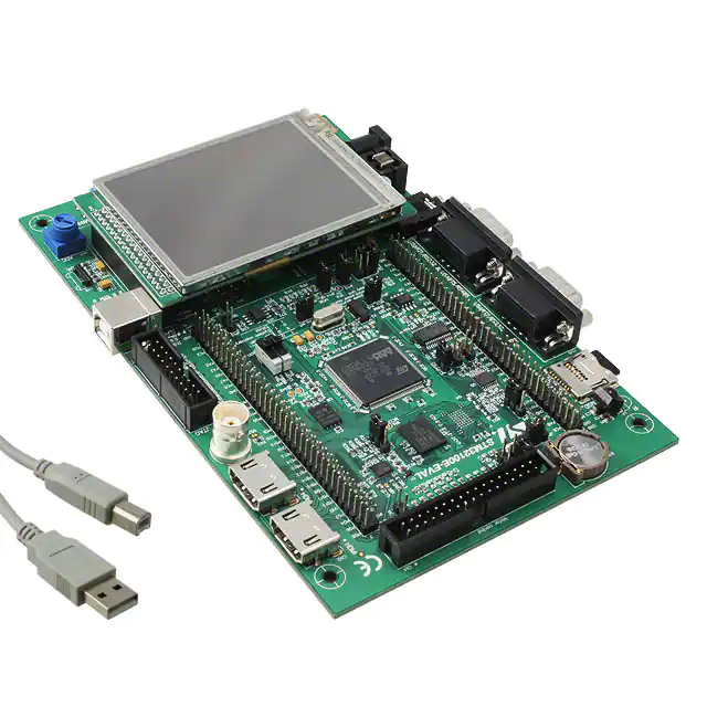
STM32100B-EVAL evaluation board
Introduction
The STM32100B-EVAL is an evaluation board for STMicroelectronics ARMTM Cortex-M3
core-based STM32F100VBT6 microcontroller. It is designed as a complete development
environment with HDMI CEC, two I2C channels, two SPI channels, three USART channels,
8 KB internal SRAM and 128 KB internal Flash, and JTAG and SWD debugging support.
With a complete range of hardware evaluations features, the STM32100B-EVAL board is
designed to help developers evaluate all device peripherals (such as HDMI CEC, motor
control, LCD, MicroSD Card™, serial Flash, speaker, IrDA and USART) and develop their
own applications. Extension connectors make it possible to easily connect a daughterboard
or wrapping board for a specific application.
An ST-LINK is integrated on the board as an embedded in-circuit debugger and programmer
for the STM32F100VBT6 MCU.
Table 1 lists the development tools concerned by this user manual.
Table 1.
Figure 1.
September 2012
Applicable tools
Type
Part number
Evaluation tool
STM32100B-EVAL
STM32F100VBT6 evaluation board (STM32100B-EVAL)
Doc ID 16533 Rev 3
1/45
www.st.com
�Contents
UM0841
Contents
1
2
Overview . . . . . . . . . . . . . . . . . . . . . . . . . . . . . . . . . . . . . . . . . . . . . . . . . . 6
1.1
Features . . . . . . . . . . . . . . . . . . . . . . . . . . . . . . . . . . . . . . . . . . . . . . . . . . . 6
1.2
Demonstration software . . . . . . . . . . . . . . . . . . . . . . . . . . . . . . . . . . . . . . . 6
1.3
Order code . . . . . . . . . . . . . . . . . . . . . . . . . . . . . . . . . . . . . . . . . . . . . . . . . 6
Hardware layout and configuration . . . . . . . . . . . . . . . . . . . . . . . . . . . . . 7
2.1
Power supply . . . . . . . . . . . . . . . . . . . . . . . . . . . . . . . . . . . . . . . . . . . . . . . 9
2.2
Boot option . . . . . . . . . . . . . . . . . . . . . . . . . . . . . . . . . . . . . . . . . . . . . . . . 10
2.3
Clock source . . . . . . . . . . . . . . . . . . . . . . . . . . . . . . . . . . . . . . . . . . . . . . . 11
2.4
Reset source . . . . . . . . . . . . . . . . . . . . . . . . . . . . . . . . . . . . . . . . . . . . . . 11
2.5
Audio . . . . . . . . . . . . . . . . . . . . . . . . . . . . . . . . . . . . . . . . . . . . . . . . . . . . 12
2.6
Serial Flash . . . . . . . . . . . . . . . . . . . . . . . . . . . . . . . . . . . . . . . . . . . . . . . 12
2.7
RS-232 . . . . . . . . . . . . . . . . . . . . . . . . . . . . . . . . . . . . . . . . . . . . . . . . . . . 12
2.8
Motor control . . . . . . . . . . . . . . . . . . . . . . . . . . . . . . . . . . . . . . . . . . . . . . 12
2.9
MicroSD Card . . . . . . . . . . . . . . . . . . . . . . . . . . . . . . . . . . . . . . . . . . . . . . 13
2.10
Temperature sensor . . . . . . . . . . . . . . . . . . . . . . . . . . . . . . . . . . . . . . . . . 13
2.11
Development and debug support . . . . . . . . . . . . . . . . . . . . . . . . . . . . . . . 13
2.12
Analog input . . . . . . . . . . . . . . . . . . . . . . . . . . . . . . . . . . . . . . . . . . . . . . . 13
2.13
IrDA . . . . . . . . . . . . . . . . . . . . . . . . . . . . . . . . . . . . . . . . . . . . . . . . . . . . . 14
2.14
Display and input devices . . . . . . . . . . . . . . . . . . . . . . . . . . . . . . . . . . . . . 14
2.15
IDD measurement . . . . . . . . . . . . . . . . . . . . . . . . . . . . . . . . . . . . . . . . . . 15
2.16
3
2/45
2.15.1
Run mode . . . . . . . . . . . . . . . . . . . . . . . . . . . . . . . . . . . . . . . . . . . . . . . 15
2.15.2
Low power mode . . . . . . . . . . . . . . . . . . . . . . . . . . . . . . . . . . . . . . . . . . 15
2.15.3
Standby or Stop IDD measurement procedure . . . . . . . . . . . . . . . . . . . 15
2.15.4
Low IDD measurement improvement procedure . . . . . . . . . . . . . . . . . . 16
HDMI CEC . . . . . . . . . . . . . . . . . . . . . . . . . . . . . . . . . . . . . . . . . . . . . . . . 16
Connectors . . . . . . . . . . . . . . . . . . . . . . . . . . . . . . . . . . . . . . . . . . . . . . . 17
3.1
Audio jack CN1 . . . . . . . . . . . . . . . . . . . . . . . . . . . . . . . . . . . . . . . . . . . . . 17
3.2
JTAG debugging connector CN3 . . . . . . . . . . . . . . . . . . . . . . . . . . . . . . . 17
3.3
Daughterboard extension connectors CN4 and CN5 . . . . . . . . . . . . . . . . 18
3.4
Motor control connector CN6 . . . . . . . . . . . . . . . . . . . . . . . . . . . . . . . . . . 22
Doc ID 16533 Rev 3
�UM0841
4
5
Contents
3.5
Analog input connector CN7 . . . . . . . . . . . . . . . . . . . . . . . . . . . . . . . . . . 23
3.6
Power supply connector CN8 . . . . . . . . . . . . . . . . . . . . . . . . . . . . . . . . . . 23
3.7
RS-232 connector CN9 with RTS/CTS handshake support . . . . . . . . . . . 24
3.8
RS-232 connector CN10 with ISP support . . . . . . . . . . . . . . . . . . . . . . . . 24
3.9
MicroSD connector CN11 . . . . . . . . . . . . . . . . . . . . . . . . . . . . . . . . . . . . . 25
3.10
ST-LINK connector CN12 . . . . . . . . . . . . . . . . . . . . . . . . . . . . . . . . . . . . . 25
3.11
ST-LINK programming connector CN13 . . . . . . . . . . . . . . . . . . . . . . . . . . 26
3.12
HDMI connectors CN15 and CN16 . . . . . . . . . . . . . . . . . . . . . . . . . . . . . 26
Limitations . . . . . . . . . . . . . . . . . . . . . . . . . . . . . . . . . . . . . . . . . . . . . . . . 27
4.1
Boot switches . . . . . . . . . . . . . . . . . . . . . . . . . . . . . . . . . . . . . . . . . . . . . . 27
4.2
PE14, PB14 and PA10 usage . . . . . . . . . . . . . . . . . . . . . . . . . . . . . . . . . . 27
4.3
Jumper JP3 . . . . . . . . . . . . . . . . . . . . . . . . . . . . . . . . . . . . . . . . . . . . . . . 27
4.4
Audio amplifier volume . . . . . . . . . . . . . . . . . . . . . . . . . . . . . . . . . . . . . . . 27
4.5
IDD standby measurement . . . . . . . . . . . . . . . . . . . . . . . . . . . . . . . . . . . . 27
Schematics . . . . . . . . . . . . . . . . . . . . . . . . . . . . . . . . . . . . . . . . . . . . . . . 28
Appendix A STM32100B-EVAL I/O assignments . . . . . . . . . . . . . . . . . . . . . . . . . 41
Revision history . . . . . . . . . . . . . . . . . . . . . . . . . . . . . . . . . . . . . . . . . . . . . . . . . . . . 44
Doc ID 16533 Rev 3
3/45
�List of tables
UM0841
List of tables
Table 1.
Table 2.
Table 3.
Table 4.
Table 5.
Table 6.
Table 7.
Table 8.
Table 9.
Table 10.
Table 11.
Table 12.
Table 13.
Table 14.
Table 15.
Table 16.
Table 17.
Table 18.
Table 19.
Table 20.
Table 21.
Table 22.
4/45
Applicable tools. . . . . . . . . . . . . . . . . . . . . . . . . . . . . . . . . . . . . . . . . . . . . . . . . . . . . . . . . . . 1
Power jumpers . . . . . . . . . . . . . . . . . . . . . . . . . . . . . . . . . . . . . . . . . . . . . . . . . . . . . . . . . . . 9
MCU power consumption measurement jumpers. . . . . . . . . . . . . . . . . . . . . . . . . . . . . . . . 10
Boot switches and jumper. . . . . . . . . . . . . . . . . . . . . . . . . . . . . . . . . . . . . . . . . . . . . . . . . . 11
Reset jumper . . . . . . . . . . . . . . . . . . . . . . . . . . . . . . . . . . . . . . . . . . . . . . . . . . . . . . . . . . . 12
Audio jumpers . . . . . . . . . . . . . . . . . . . . . . . . . . . . . . . . . . . . . . . . . . . . . . . . . . . . . . . . . . . 12
Motor control jumpers . . . . . . . . . . . . . . . . . . . . . . . . . . . . . . . . . . . . . . . . . . . . . . . . . . . . . 13
IrDA jumper. . . . . . . . . . . . . . . . . . . . . . . . . . . . . . . . . . . . . . . . . . . . . . . . . . . . . . . . . . . . . 14
240x320 TFT color LCD modules . . . . . . . . . . . . . . . . . . . . . . . . . . . . . . . . . . . . . . . . . . . . 14
HDMI CEC solder bridge . . . . . . . . . . . . . . . . . . . . . . . . . . . . . . . . . . . . . . . . . . . . . . . . . . 16
JTAG debugging connector . . . . . . . . . . . . . . . . . . . . . . . . . . . . . . . . . . . . . . . . . . . . . . . . 17
Daughterboard extension connector CN4 . . . . . . . . . . . . . . . . . . . . . . . . . . . . . . . . . . . . . 18
Daughterboard extension connector CN5 . . . . . . . . . . . . . . . . . . . . . . . . . . . . . . . . . . . . . 20
Motor control connector CN6 . . . . . . . . . . . . . . . . . . . . . . . . . . . . . . . . . . . . . . . . . . . . . . . 22
Analog input connector CN7 . . . . . . . . . . . . . . . . . . . . . . . . . . . . . . . . . . . . . . . . . . . . . . . 23
RS-232 connector CN9 with full modem control support . . . . . . . . . . . . . . . . . . . . . . . . . . 24
RS-232 connector CN10. . . . . . . . . . . . . . . . . . . . . . . . . . . . . . . . . . . . . . . . . . . . . . . . . . . 24
MicroSD connector CN11 . . . . . . . . . . . . . . . . . . . . . . . . . . . . . . . . . . . . . . . . . . . . . . . . . . 25
ST-LINK USB connector (CN12) . . . . . . . . . . . . . . . . . . . . . . . . . . . . . . . . . . . . . . . . . . . . 25
HDMI connectors (CN15 and CN16) . . . . . . . . . . . . . . . . . . . . . . . . . . . . . . . . . . . . . . . . . 26
Missing resistors on PCB rev A . . . . . . . . . . . . . . . . . . . . . . . . . . . . . . . . . . . . . . . . . . . . . 27
STM32100B-EVAL I/O assignments . . . . . . . . . . . . . . . . . . . . . . . . . . . . . . . . . . . . . . . . . 41
Doc ID 16533 Rev 3
�UM0841
List of figures
List of figures
Figure 1.
Figure 2.
Figure 3.
Figure 4.
Figure 5.
Figure 6.
Figure 7.
Figure 8.
Figure 9.
Figure 10.
Figure 11.
Figure 12.
Figure 13.
Figure 14.
Figure 15.
Figure 16.
Figure 17.
Figure 18.
Figure 19.
Figure 20.
Figure 21.
Figure 22.
Figure 23.
Figure 24.
Figure 25.
Figure 26.
STM32F100VBT6 evaluation board (STM32100B-EVAL) . . . . . . . . . . . . . . . . . . . . . . . . . . 1
Hardware block diagram . . . . . . . . . . . . . . . . . . . . . . . . . . . . . . . . . . . . . . . . . . . . . . . . . . . . 7
STM32100B-EVAL board layout. . . . . . . . . . . . . . . . . . . . . . . . . . . . . . . . . . . . . . . . . . . . . . 8
STM32100B-EVAL IDD measurement circuit . . . . . . . . . . . . . . . . . . . . . . . . . . . . . . . . . . . 15
STM32100B-EVAL IDD low power mode measurement timing diagram . . . . . . . . . . . . . . 16
JTAG debugging connector CN3 (front view) . . . . . . . . . . . . . . . . . . . . . . . . . . . . . . . . . . . 17
Motor control connector CN6 (top view) . . . . . . . . . . . . . . . . . . . . . . . . . . . . . . . . . . . . . . . 22
Analog input connector CN7 (bottom view) . . . . . . . . . . . . . . . . . . . . . . . . . . . . . . . . . . . . 23
Power supply connector CN8 (front view) . . . . . . . . . . . . . . . . . . . . . . . . . . . . . . . . . . . . . 23
RS-232 connector CN9 with RTS/CTS handshake support (front view). . . . . . . . . . . . . . . 24
RS-232 connector CN10 (front view) . . . . . . . . . . . . . . . . . . . . . . . . . . . . . . . . . . . . . . . . . 24
MicroSD connector CN11 (top view) . . . . . . . . . . . . . . . . . . . . . . . . . . . . . . . . . . . . . . . . . 25
ST-LINK connector CN12 (front view) . . . . . . . . . . . . . . . . . . . . . . . . . . . . . . . . . . . . . . . . 25
HDMI connectors CN15 and CN16. . . . . . . . . . . . . . . . . . . . . . . . . . . . . . . . . . . . . . . . . . . 26
Evaluation board schematics . . . . . . . . . . . . . . . . . . . . . . . . . . . . . . . . . . . . . . . . . . . . . . . 29
MCU . . . . . . . . . . . . . . . . . . . . . . . . . . . . . . . . . . . . . . . . . . . . . . . . . . . . . . . . . . . . . . . . . . 30
Peripherals . . . . . . . . . . . . . . . . . . . . . . . . . . . . . . . . . . . . . . . . . . . . . . . . . . . . . . . . . . . . . 31
RS-232 . . . . . . . . . . . . . . . . . . . . . . . . . . . . . . . . . . . . . . . . . . . . . . . . . . . . . . . . . . . . . . . . 32
Audio . . . . . . . . . . . . . . . . . . . . . . . . . . . . . . . . . . . . . . . . . . . . . . . . . . . . . . . . . . . . . . . . . 33
Joystick, LCD, tamper button, wakeup button, user button . . . . . . . . . . . . . . . . . . . . . . . . 34
MicroSD Card and Flash . . . . . . . . . . . . . . . . . . . . . . . . . . . . . . . . . . . . . . . . . . . . . . . . . . 35
Motor control . . . . . . . . . . . . . . . . . . . . . . . . . . . . . . . . . . . . . . . . . . . . . . . . . . . . . . . . . . . . 36
JTAG and SWD debugger . . . . . . . . . . . . . . . . . . . . . . . . . . . . . . . . . . . . . . . . . . . . . . . . . 37
Power supply . . . . . . . . . . . . . . . . . . . . . . . . . . . . . . . . . . . . . . . . . . . . . . . . . . . . . . . . . . . 38
ST-LINK . . . . . . . . . . . . . . . . . . . . . . . . . . . . . . . . . . . . . . . . . . . . . . . . . . . . . . . . . . . . . . . 39
2.4 inch color LCD board . . . . . . . . . . . . . . . . . . . . . . . . . . . . . . . . . . . . . . . . . . . . . . . . . . 40
Doc ID 16533 Rev 3
5/45
�Overview
UM0841
1
Overview
1.1
Features
1.2
●
Three 5 V power supply options: power jack, ST-LINK connector or daughterboard
●
Boot from user Flash, system memory or SRAM
●
Speaker
●
1 Gbyte MicroSD Card™
●
16 Mbyte serial Flash
●
I2C/SMBus compatible serial interface temperature sensor
●
Two RS-232 communication channels with support for RTS/CTS handshake on one
channel
●
IrDA transceiver
●
Induction motor control connector
●
JTAG and SWD debug support
●
240x320 TFT color LCD
●
Joystick with 4-direction control and selector
●
Reset, wakeup, tamper and user push buttons
●
Four LEDs
●
RTC with backup battery
●
Extension connector for daughterboard or wrapping board
●
Embedded ST-LINK
●
IDD current measurement circuit
●
HDMI CEC
Demonstration software
Demonstration software is preloaded in the board's Flash memory for easy demonstration of
the device peripherals in stand-alone mode. For more information and to download the
latest version available, please refer to the STM32100B-EVAL demonstration software
available on www.st.com.
1.3
Order code
To order the STM32F100VBT6 evaluation board, use the order code STM32100B-EVAL.
6/45
Doc ID 16533 Rev 3
�UM0841
2
Hardware layout and configuration
Hardware layout and configuration
The STM32100B-EVAL board is designed around a STM32F100VBT6 microcontroller in a
100-pin LQFP package.
The hardware block diagram Figure 2 shows the connections between the
STM32F100VBT6 microcontroller and the peripherals (LCD, SPI Flash, USART, IrDA,
speaker, HDMI CEC, temperature sensor, MicroSD Card, motor control and embedded STLINK).
Figure 3 will help you locate these features on the evaluation board.
Figure 2.
Hardware block diagram
30)�
($-)
CONNECTOR�
($-)
CONNECTOR�
)�#�
30)�
#%#
-ICRO3$
#ARD
*OYSTICK
,%$S
'0)/
".#
CONNECTOR
!$#
)R$!
TRANSCEIVER
53!24�
23
���
TRANSCEIVER
53!24�
$"�CONNECTOR
53!24�
23
���
TRANSCEIVER
53!24�
$"�CONNECTOR
!$#
$!#
-OTOR#ONTROL
CONNECTOR
-#
4EMPERATURE
SENSOR
)�#�
3ERIAL&LASH
53!24�
34-��&���6"4�
"UTTONS
4&4COLOR
,#$
*4!'
0OTENTIOMETER
���6REGULATOR
3PEAKER
AMPLIFIER
%MBEDDED
34
,).+
53"4YPE"
CONNECTOR
*4!'�4RACE
CONNECTOR
Doc ID 16533 Rev 3
-#5
CONSUMPTION
MEASUREMENT
%XTENSION
CONNECTORFOR
'0)/S
7/45
�Hardware layout and configuration
Figure 3.
UM0841
STM32100B-EVAL board layout
CN4, CN5
Extension connector
CN6
Motor control
CN7
BNC
CN9
USART2
CN16
HDMI
connector
U3
VALUELINE
CN15
HDMI
connector
CN10
USART1
CN3
JTAG
RV1
Potentiometer
CN11
MicroSD
CN12
ST-LINK
U14
Color LCD
U14
IrDA
CN1
Audio jack
CN8
Power jack
RV2
Potentiometer
8/45
B1
RESET
B2
WAKEUP
B3
Tamper
Doc ID 16533 Rev 3
U4
Joystick
B4
Key
�UM0841
2.1
Hardware layout and configuration
Power supply
The STM32100B-EVAL board is designed to be powered by a 5 V DC power supply and to
be protected by PolyZen U10 in case of incorrect power supply configuration.
It is possible to configure the evaluation board to use any of the following sources for the
power supply:
●
5 V DC power adapter connected to CN8, the power supply jack labeled “PSU” (for
power supply unit) on the silkscreen.
●
5 V DC power with 500 mA limitation from CN12, the ST-LINK type-B USB connector
labeled “USB” on the silkscreen.
●
5 V DC power from both CN4 and CN5, the daughterboard extension connectors
labeled “DTB” (for daughterboard) on the silkscreen.
The power supply is configured by setting jumpers JP9 and JP10 as described in Table 2.
Table 2.
Jumper
Description
JP10 is used to select one of the three possible power supply resources.
For power supply from the power supply jack (CN8) to the
STM32100B-EVAL only, JP10 is set as shown:
PSU
DTB
USB
For power supply from the daughterboard connectors (CN4 and CN5)
to the STM32100B-EVAL only, JP10 is set as shown:
PSU
DTB
USB
For power supply from the ST-LINK USB connector (CN12) to the
STM32100B-EVAL only, JP10 is set as shown (default setting):
PSU
DTB
USB
JP10
Power jumpers
PSU
DTB
USB
For power supply from power supply jack (CN8) to both the
STM32100B-EVAL board and to a daughterboard connected on CN4
and CN5, JP10 is set as shown: The daughterboard must not have its
own power supply connected.
Vbat is connected to VDD_MCU power when JP9 is set as shown (default
setting):
1 2 3
Vbat is connected to battery when JP9 is set as shown:
1 2 3
JP9
Caution:
Risk of explosion if battery is replaced by an incorrect one. Dispose of used batteries
according to the instructions.
To enable MCU power consumption measurement, JP8 and JP12 should be re-configured
as described in Table 3. (PCB rev B only. See Section 4.5: IDD standby measurement for
details.)
LED LD5 is lit when the STM32100B-EVAL board is correctly powered by 5 V.
Doc ID 16533 Rev 3
9/45
�Hardware layout and configuration
Note:
UM0841
The AC220V to DC5V power adapter PSU-5V2A (recommended and can be ordered from
ST, it is not provided with board by default) or equivalent power adapter (polarity compatible
with CN8) can be used to power STM32100B-EVAL board via power jack CN8 on the board.
To order the recommended power supply, use the order code PSU-5C2A.
Table 3.
MCU power consumption measurement jumpers
Jumper
Description
VDD power is directly connected to MCU VDD when JP8 is set as shown:
1 2 3
(Default setting)
Note: For manual IDD measurement JP8 must be removed and replaced by an ammeter
connected between JP8 pins 1 and 2.
JP8
Connect VDD power to MCU with current-sampling resistor, 1Ω or 1KΩ, in
series for IDD current measurement when JP8 is set as shown:
JP12
2.2
1 2 3
(Available only on PCB rev B.) Connect IDD_CNT_EN (PE14) to Anti-tamper (PC13) for
IDD current measurement in standby mode when JP12 is closed.
Default setting: Not fitted
Boot option
The STM32100B-EVAL board can boot from:
●
Embedded user Flash
●
System memory with boot loader for ISP
●
Embedded SRAM for debugging
The boot option is configured by switches SW1 and SW2 as shown in Table 4.
Note:
10/45
The hardware implementation of JP4 and the RS-232 interface can be only used when the
Boot0 is at a high level through the onboard switch SW2, which is not the most common
case of usage.
Doc ID 16533 Rev 3
�UM0841
Hardware layout and configuration
Boot switches and jumper
Boot from
Switch configuration
JP4
2.3
0 1
SW1
Boot 1
STM32100B-EVAL boots from system memory when SW1 and
SW2 are set as shown to the right.
SW1
Boot 1
STM32100B-EVAL boots from embedded SRAM when SW1 and
SW2 are set as shown to the right.
SW2
Boot 0
SW2
SW2
Boot 0
SW1
0 1
STM32100B-EVAL boots from user Flash when SW2 is set as
shown to the right (default setting).
In this configuration, the position of SW1 does not affect the boot
process.
0 1
Switch
SW2
Boot 0
Table 4.
BOOT0 pin of the STM32F100VBT6 is connected to the RS-232
connector CN10 pin 8 (CTS) for ISP support when JP4 is closed.
This configuration is used for boot loader application only.
Default setting: not fitted.
Clock source
Two clock sources are available on the STM32100B-EVAL board for the STM32F100VBT6
microcontroller and RTC.
2.4
●
X1, 32 KHz crystal for embedded RTC
●
X2, 8 MHz crystal with socket for the STM32F100VBT6 microcontroller. It can be
removed from the socket when the internal RC clock is used.
Reset source
The reset signal of the STM32100B-EVAL board is active low and the reset sources include:
●
Reset button B1
●
Debugging tools from JTAG connector CN3
●
Daughterboard from CN5
●
Embedded ST-LINK
●
Bootloader_Reset from RS-232 connector CN10
Doc ID 16533 Rev 3
11/45
�Hardware layout and configuration
Table 5.
2.5
UM0841
Reset jumper
Jumper
Description
JP5
Bootloader_Reset signal from the RS-232 connector CN10 pin 1 (DCD) is connected
to RESET# of the STM32F100VBT6 when JP5 is closed.
This configuration is used for the boot loader application only.
Default setting: Not fitted
Audio
The STM32100B-EVAL board supports playback based on a speaker on the board. This
can be disabled or enabled by jumpers JP1 and JP2. The audio volume can be adjusted
using the potentiometer RV1. See Section 4.4: Audio amplifier volume.
Table 6.
Audio jumpers
Jumper
2.6
Description
JP1
Audio power amplifier TS4990IST is forced on standby mode when JP1 is fitted.
Default setting: Not fitted
JP2
The DAC _OUT(PA4) is connected to speaker circuit when JP2 is closed.
Default setting: Fitted
Serial Flash
A 128 Mbit serial Flash connected to SPI1 of the STM32F100VBT6 microcontroller shares
the same SPI port with the MicroSD Card using a different chip select signal. Serial Flash
chip select is managed by the standard I/O port PD9.
2.7
RS-232
Two type D 9-pin connectors, CN10 (USART1) and CN9 (USART2) are available on the
STM32100B-EVAL board.
2.8
●
CN10 connects to the RS-232 transceiver U15 with Bootloader_Reset and
Bootloader_BOOT0 support.
●
CN9 connects to the RS-232 transceiver U13 with RTS/CTS handshake signal support.
Motor control
The STM32100B-EVAL board supports induction motor control via a 34-pin connector, CN6,
which provides all required control and feedback signals to and from a motor power-drive
board. Available signals on this connector include emergency stop, motor speed, 3-phase
motor current, bus voltage, heat sink temperature coming from the motor drive board and 6
channels of PWM control signals going to the motor drive circuit.
Special motor current sampling operation is enabled by setting jumper JP7.
Note:
12/45
On MB871 PCB rev A MC_CurrentA shares PC1 with VBAT_ADCIN through JP3 so the
jumper JP3 must be removed for motor control applications. See Section 4.3: Jumper JP3.
Doc ID 16533 Rev 3
�UM0841
Hardware layout and configuration
Table 7.
Motor control jumpers
Jumper
2.9
Description
JP7
The special motor current sampling operation is enabled when JP7 is fitted (PD2
connected to PB0). The I/O pins PD2 and PB0 are disconnected and can be used by
daughterboard when JP7 is not fitted.
Default setting: Not fitted
JP6
JP6 should be kept open when encoder signal is from pin 31 of motor control connector
CN6. It should be kept closed when analog signal is from pin 31 of CN6 for special motor.
Default setting: Not fitted (open)
MicroSD Card
The 1 Gbyte MicroSD Card connected to SPI1 of the STM32F100VBT6 microcontroller
(shared with serial Flash), is available on the board. MicroSD Card chip selection is
managed by the standard I/O port PC12 while the MicroSD card defect signal is managed
by I/O port PE7.
2.10
Temperature sensor
One I2C interface temperature sensor STLM75 (–55°C to +125°C) connected to I2C1 of the
STM32F10x microcontroller, is available on the board.
2.11
Development and debug support
An embedded ST-LINK STM32 JTAG interface developed by STMicroelectronic’s is
available on the STM32100B-EVAL as the default debugger hardware interface.
Of course, third-party debugger interfaces are also supported by the JTAG connector CN3.
2.12
Analog input
One BNC connector, CN7, is connected to PA4 of the STM32F100VBT6 microcontroller as
an external analog input. or DAC output. The 50Ω terminal resistor can be enabled by
closing solder bridge SB1. A low pass filter can be implemented for the BNC connector by
replacing R44 and C33 for ADC input, or replacing R43 and C33 for DAC output with the
correct value of resistor and capacitor as requested by the end user's application.
There are also 3 analog signals available on the board:
1.
10 KΩ potentiometer RV2 connected to PC4.
2.
IDD measurement output signal connected to PC5 for MCU power consumption test.
3.
External ADC input which can be connected to TP3 (AIN+) and TP2 (AIN-), R45 should
be removed to avoid noise.
Doc ID 16533 Rev 3
13/45
�Hardware layout and configuration
2.13
UM0841
IrDA
IrDA communication is supported by the IrDA transceiver U14, which is connected to
USART3 of the STM32F100VBT6 microcontroller. It is enabled or disabled by jumper JP11.
Table 8.
IrDA jumper
Jumper
JP11
2.14
Description
Enables/disables the IrDA transceiver. IrDA is enabled when JP11 is fitted, and disabled
when JP11 is not fitted.
Default setting: Fitted
Display and input devices
The 240x320 TFT color LCD (mounted on connector CN14) and 4 general purpose LEDs
(LD1, 2, 3, 4) are available as display devices.
A 4-direction joystick with selection key, general purpose push button (B4), wakeup button
(B2) and tamper detection button (B3) are available as input devices.
Table 9.
CN14 pin
14/45
240x320 TFT color LCD modules
Description
Pin connection
CN14 pin
Description
Pin connection
1
CS
PB2
9
VDD
+3V3
2
SCL
PB13
10
VCI
+3V3
3
SDI
PB15
11
GND
GND
4
RS
12
GND
GND
5
WR
13
BL_VDD
+3V3
6
RD
14
BL_Control
PA8
7
SDO
PB14
15
BL_GND
GND
8
RESET#
RESET#
16
BL_GND
GND
Doc ID 16533 Rev 3
�UM0841
2.15
Hardware layout and configuration
IDD measurement
For IDD measurement the circuit below is implemented on the STM32100B-EVAL.
Figure 4.
STM32100B-EVAL IDD measurement circuit
2.15.1
Run mode
In Run mode, IDD current is measured using MAX9938FEUK+ (U6) connected to the 1Ω
shunt resistor (R71). In this case IDD_CNT_EN remains high during measurement and a
jumper must be connected between pins 2 and 3 of JP8.
2.15.2
Low power mode
In low power modes (Stop or Standby), the operational amplifier MAX9938FEUK+ (U6) is
connected to the 1KΩ shunt resistor (R72), controlled by the analogue switch STT5PF20V
(T2). In this case the counter 74HC4060 (U9) enabled by IDD_CNT_EN manages the
measurement timing according to Figure 5.
2.15.3
Standby or Stop IDD measurement procedure
To measure a current corresponding to the low power mode the procedure is:
1.
Configure ADC to measure voltage on IDD_measurement pin.
2.
Configure PA0 as wakeup pin.
3.
Enter in Low Power mode after configuring IDD_CNT_EN Low as output low level
(PC13 if JP12 is closed, or PE14 if JP12 is open or on MB871 rev A).
4.
LP_WAKEUP rising edge wakeup the MCU after around 150 ms.
5.
Start ADC conversion as soon as possible after wakeup in order to measure the
voltage corresponding to Low Power mode on capacitor C41.
6.
Reset the counter by programming IDD_CNT_EN High in less than 70 ms after the
wakeup to avoid 1 KΩ being connected later on VDD_MCU.
Doc ID 16533 Rev 3
15/45
�Hardware layout and configuration
UM0841
In low power mode, the 1 KΩ resistor is connected when T2 goes off after entering low
power mode. Q13 output of the counter allows connection of the 1KΩ resistor when the
current IDD becomes very low. The measurement timing is given in Figure 5.
Figure 5.
STM32100B-EVAL IDD low power mode measurement timing diagram
Low pow er mode IDD measurement timing
Run
W ake-u p
L ow p o wer
ID D Measu re
C lear C N T
MCU mo d e
0
150mS
300mS
450mS
ID D _C N T_EN
Q13 = L OW _POW ER _EN
(T2 p in 3)
Q14 = L P_W AK EU P
Q14n = U 7 p in 4
The low power mode measurement procedure can be used in Standby or Stop mode if the
IDD current does not exceed 60 uA, otherwise the Run mode measurement procedure
should be used up to 60 mA.
Note:
2.15.4
1
The standby current measure is not possible on MB871 rev A as explained in chapter 3.5
IDD standby measure.
2
In standby mode the bias current of operational amplifier input (U6 pin 4) is not negligible
compared to IDD current (Typical I bias is ~200 nA). To improve the IDD measurement
precision it mandatory to subtract the I bias current to the IDD standby measure since this
current is not sink by the MCU. It is possible to measure I bias (U1 pin 4 current) and to
subtract this value to MCU current.
Low IDD measurement improvement procedure
The procedure for precision IDD measurement is:
2.16
1.
Place a jumper on JP8 pins 1 and 2.
2.
Follow the low power mode procedure to measure I1 = I bias.
3.
Remove jumper JP8 pins 1 and 2 and place it on JP8 pins 2 and 3.
4.
Follow the low power mode procedure to measure I2 = IDD + I bias.
5.
Calculate actual IDD: IDD = I2 - I1.
HDMI CEC
Two HDMI connectors CN15 and CN16 are available on the STM32100B-EVAL board. The
signals CEC, SCL, SDA and HPD are supported and connected to the STM32F100VBT6
through HDMI2C1-5DIJ, the ST full integrated ESD protection, level-shifting device and
signal booster for control links of the HDMI 1.3 transmitter.
Table 10.
Jumper
SB4
16/45
HDMI CEC solder bridge
Description
The +5 V power pin of HDMI connectors CN15 and CN16 is connected to 5 V power on the
STM32100B-EVAL board when SB4 is closed. Default status: Open
Doc ID 16533 Rev 3
�UM0841
Connectors
3
Connectors
3.1
Audio jack CN1
A 3.5 mm mono audio jack CN1 is available on the STM32100B-EVAL board. The speaker
U12 is bypassed when earphones are plugged into CN8.
3.2
JTAG debugging connector CN3
Figure 6.
JTAG debugging connector CN3 (front view)
Table 11.
19 17 15 13 11 9 7 5
3
1
20 18 16 14 12 10 8 6
4
2
JTAG debugging connector
Pin number
Description
Pin number
Description
1
3.3V power
2
3.3V power
3
TRST
4
GND
5
TDI
6
GND
7
TMS/SWDIO
8
GND
9
TCK/SWCLK
10
GND
11
RTCK
12
GND
13
TDO/SWO
14
GND
15
RESET#
16
GND
17
Pull-Down
18
GND
19
Pull-Down
20
GND
Doc ID 16533 Rev 3
17/45
�Connectors
3.3
UM0841
Daughterboard extension connectors CN4 and CN5
Two 50-pin male headers, CN4 and CN5, can connect a daughterboard or standard
wrapping board to the STM32100B-EVAL board. All GPIOs are available on these
connectors. The space between these two connectors and position of power, GND and
RESET pin is defined as a standard (which allows to develop common daughterboards for
several evaluation boards). Moreover all I/O on these connectors are pinout compatible with
the STM3210B-EVAL board (except PC14 and PC15 which do not exist on the
STM32F103VBT6). The standard width between CN4 pin1 and CN5 pin1 is 2700 mils
(68.58mm). The standard was implemented on the majority of evaluation boards. Each pin
on CN4 and CN5 can be used by a daughterboard after disconnecting it from the
corresponding function block on the STM32100B-EVAL board. Refer to Table 12 and
Table 13 for details.
Table 12.
Daughterboard extension connector CN4
Pin Description
18/45
Alternate function
How to disconnect from function block on
STM32100B-EVAL board
1
GND
-
-
3
PC1
MC connector pin15
Disconnect STM32100B-EVAL evaluation board
from motor power drive board
5
PC3
MC connector pin 19
Disconnect STM32100B-EVAL evaluation board
from motor power drive board
7
PA1
MC connector pin 33
Disconnect STM32100B-EVAL evaluation board
from motor power drive board
9
PA3
MC connector pin 14
Disconnect STM32100B-EVAL evaluation board
from motor power drive board
11
PA4
Audio_DAC / BNC
Keep JP2 on open
13
PA6
SPI Flash& MicroSD card
Remove R89
15
PC4
Potentiometer RV2
Remove R48
17
PB0
MC connector pin 27
Keep JP7 on open
19
GND
-
-
21
PE7
MicroSD card detect
Remove card from CN11 or remove R91
23
PE9
MC connector pin 3
Disconnect STM32100B-EVAL evaluation board
from motor power drive board
25
PE11
MC connector pin 7
Disconnect STM32100B-EVAL evaluation board
from motor power drive board
27
PE13
MC connector pin 11
Disconnect STM32100B-EVAL evaluation board
from motor power drive board
29
PE15
MC connector pin 1
Remove R24
31
PC14
OSC32_IN
Keep SB2 on close and remove R17
33
PB10
HDMI_SCL
Remove R108
35
PB13
LCD_CLK
-
37
PB15
LCD_MOSI
-
39
GND
-
-
Doc ID 16533 Rev 3
�UM0841
Connectors
Table 12.
Daughterboard extension connector CN4 (continued)
Pin Description
Alternate function
How to disconnect from function block on
STM32100B-EVAL board
41
PD9
Flash_CS
-
43
PD11
-
-
45
PD13
MC connector pin 23
Disconnect STM32100B-EVAL evaluation board
from motor power drive board
47
PD15
-
-
49
D5V
-
-
2
PC0
MC connector pin 26
Disconnect STM32100B-EVAL evaluation board
from motor power drive board
4
PC2
MC connector pin 17
Disconnect STM32100B-EVAL evaluation board
from motor power drive board
6
PA0
MC connector pin 31 &
Wakeup button
Disconnect STM32100B-EVAL evaluation board
from motor power drive board.
Remove R58
8
PA2
MC connector pin 34
Disconnect STM32100B-EVAL evaluation board
from motor power drive board
10
GND
-
-
12
PA5
SPI Flash & MicroSD card
-
14
PA7
SPI Flash & MicroSD card
-
16
PC5
IDD_measurement
Remove R70
18
PB1
MC connector pin 29
Disconnect STM32100B-EVAL evaluation board
from motor power drive board
20
PB2
BOOT1 & LCD
-
22
PE8
MC connector pin 5
Disconnect STM32100B-EVAL evaluation board
from motor power drive board
24
PE10
MC connector pin 9
Disconnect STM32100B-EVAL evaluation board
from motor power drive board
26
PE12
MC connector pin 13
Disconnect STM32100B-EVAL evaluation board
from motor power drive board
28
PE14
IDD_CNT_EN
Remove R117 (does not exist on PCB rev A)
30
GND
-
-
32
PC15
OSC32_OUT
Keep SB3 on close and remove R17
34
PB11
HDMI_SDA
Remove R109
36
PB12
HDMI_HPD
Remove R110
38
PB14
LCD_MISO
Remove R116 (does not exist on PCB rev A)
40
PD8
Joystick Up
Remove R42
42
PD10
MC connector pin 21
Disconnect STM32100B-EVAL evaluation board
from motor power drive board
44
PD12
Joystick selection
Remove R38
Doc ID 16533 Rev 3
19/45
�Connectors
UM0841
Table 12.
Daughterboard extension connector CN4 (continued)
Pin Description
Alternate function
46
PD14
Joystick Down
Remove R39
48
+3V3
-
-
50
GND
-
-
Table 13.
Daughterboard extension connector CN5
Pin Description
20/45
How to disconnect from function block on
STM32100B-EVAL board
How to disconnect from component on
STM32100B-EVAL board
Alternate function
1
GND
-
-
3
NC
-
5
PE6
-
-
7
PE4
-
-
9
PC13
Tamper Key
Remove R37
11
RESET#
RESET# button
-
13
PE1
Joystick Right
Remove R41
15
PB9
User button
Remove R46
17
PB7
Temperature sensor_SDA
Remove R47
19
D5V
-
-
21
PB4
Debug nTRST
-
23
NC
-
-
25
PD6
USART2_RX
Remove R81
27
PD4
USART2_RTS
Remove R15
29
PD3
USART2_CTS
Remove R82
31
PD1
-
-
33
PC12
MicroSD card_CS
Remove R90
35
PC10
IrDA_TX
-
37
PA14
Debug TCK/SWCLK
-
39
GND
-
-
41
PA12
-
-
43
PA10
USART1_RX
Remove R115 (not existent on PCB rev A)
45
PA8
MCO
-
47
PC8
LED3
Remove R61
49
PC6
LED1
Remove R59
2
NC
4
PC13
Tamper button
Remove R637
Doc ID 16533 Rev 3
�UM0841
Connectors
Table 13.
Daughterboard extension connector CN5 (continued)
Pin Description
How to disconnect from component on
STM32100B-EVAL board
Alternate function
6
PE5
-
-
8
PE3
-
-
10
GND
-
-
12
PE2
-
-
14
PE0
Joystick Left
Remove R40
16
PB8
HDMI_CEC
Remove R107
18
PB6
Temperature sensor_SCL
Remove R49
20
PB5
Temperature sensor_INT
Remove R50
22
PB3
Debug TDO/SWO
-
24
NC
-
-
26
PD7
-
-
28
PD5
USART2
Remove R9
30
GND
-
-
32
PD2
MC connector pin 27
Disconnect STM32100B-EVAL evaluation board
from motor power drive board.
Keep JP7 on open
34
PD0
-
-
36
PC11
IrDA_RX
Remove R83
38
PA15
Debug TDI
-
40
PA13
Debug TMS/SWDIO
-
42
PA11
LCD_Backlight
-
44
PA9
USART1_TX
Remove R16
46
PC9
LED4
Remove R62
48
PC7
LED2
Remove R60
50
GND
-
-
Doc ID 16533 Rev 3
21/45
�Connectors
3.4
UM0841
Motor control connector CN6
Figure 7.
Table 14.
Motor control connector CN6 (top view)
33 31 29 27 25 23 21 19 17 15 13 11 9 7 5
3
1
34 32 30 28 26 24 22 20 18 16 14 12 10 8 6
4
2
Motor control connector CN6
Description
STM32F100VBT6
pin
STM32F100VBT6
pin
Description
Emergency stop
PE15
1
2
GND
PWM-UH
PE9
3
4
GND
PWM-UL
PE8
5
6
GND
PWM-VH
PE11
7
8
GND
PWM-VL
PE10
9
10
GND
PWM-WH
PE13
11 12
GND
PWM-WL
PE12
13 14
PHASE A current
PC1
15 16
GND
PHASE B current
PC2
17 18
GND
PHASE C current
PC3
19 20
GND
NTC bypass relay
PD10
21 22
GND
Dissipative brake PWM
PD13
23 24
GND
+5 V power
22/45
CN6
pin
25 26
PA3
PC0
Bus voltage
Heatsink temperature
PFC SYNC
PD2/PB0
27 28
3.3 V power
PFC PWM
PB1
29 30
GND
Encoder A
PA0
31 32
GND
Encoder B
PA1
33 34
Doc ID 16533 Rev 3
PA2
Encoder index
�UM0841
3.5
Connectors
Analog input connector CN7
Figure 8.
Analog input connector CN7 (bottom view)
1
2
5
4
Table 15.
Analog input connector CN7
Pin number
3.6
3
Description
Pin number
Description
1
GND
4
GND
2
GND
5
Analog input/PA4
3
GND
Power supply connector CN8
The STM32100B-EVAL board can be powered from a DC 5 V power supply via the external
power supply jack (CN8) shown in Figure 9. The central pin of CN8 must be positive.
Figure 9.
Power supply connector CN8 (front view)
DC +5V
GND
Doc ID 16533 Rev 3
23/45
�Connectors
3.7
UM0841
RS-232 connector CN9 with RTS/CTS handshake support
Figure 10. RS-232 connector CN9 with RTS/CTS handshake support (front view)
Table 16.
RS-232 connector CN9 with full modem control support
Pin number
3.8
Description
Pin number
Description
1
NC
6
Connect to Pin 4
2
USART2_RX
7
USART2_RTS
3
USART2_TX
8
USART2_CTS
4
Connect to Pin 6
9
NC
5
GND
RS-232 connector CN10 with ISP support
Figure 11. RS-232 connector CN10 (front view)
Table 17.
RS-232 connector CN10
Pin number
24/45
Description
Pin number
Description
1
Bootloader_Reset
6
NC
2
USART1_RX
7
NC
3
USART1_TX
8
Bootloader_BOOT0
4
NC
9
NC
5
GND
Doc ID 16533 Rev 3
�UM0841
3.9
Connectors
MicroSD connector CN11
Figure 12. MicroSD connector CN11 (top view)
Table 18.
MicroSD connector CN11
Pin number
3.10
Description
Pin number
Description
1
Reserved
5
SCLK/PA5
2
CS/PC12
6
Vss/GND
3
DI/PA7
7
DO/PA6
4
VDD
8, 9
Card detect (PE7)
ST-LINK connector CN12
Figure 13. ST-LINK connector CN12 (front view)
5
Table 19.
6
ST-LINK USB connector (CN12)
Pin number
Description
Pin number
Description
1
VBUS (power)
4
GND
2
DM
5
Shield
3
DP
6
Shield
Doc ID 16533 Rev 3
25/45
�Connectors
3.11
UM0841
ST-LINK programming connector CN13
The connector CN13 is not mounted on the board and is reserved for manufacture only.
3.12
HDMI connectors CN15 and CN16
Figure 14. HDMI connectors CN15 and CN16
Table 20.
HDMI connectors (CN15 and CN16)
Pin number
26/45
Description
Pin number
Description
1-12
NC
16
SDC (PB11)
13
CEC (PB8)
17
GND
14
NC
18
NC
15
SCL (PB10)
19
HPD (PB12)
Doc ID 16533 Rev 3
�UM0841
4
Limitations
Limitations
The MB871 board is delivered with PCB revision A or B. The PCB version is mentioned on
the bottom right corner of the board. Both versions of PCB are fully compatible in
configuration by default but several limitations on the PCB rev A are removed on PCB rev B.
All PCB rev A limitations are explained in this chapter.
4.1
Boot switches
On PCB rev A, boot switches SW1 and SW2 are not referenced on the silkscreen. SW1
(Boot1) switch is located in the right position on the board and SW2 (Boot0) in left position.
4.2
PE14, PB14 and PA10 usage
When a daughterboard is connected to CN4, CN5 (extension connectors) if PE14, PB14 or
PA10 are used on the daughterboard it is not possible to disconnect the signals assigned to
these I/Os on the motherboard (MB871 rev A). On PCB rev B 0Ω resistors are placed on
these signals allowing them to be disconnected when these I/O are used on the
daughterboard.
Table 21.
4.3
Missing resistors on PCB rev A
Resistor
Signal name
R115
PA10
R116
PB14
R117
PE14
Jumper JP3
On PCB rev A, JP3 can connect VBAT to PC1 with a jumper for battery voltage
measurement using ADC_IN11. JP3 jumper must not be used to avoid unexpected current
consumption on the battery when the board is not powered.
Note:
The pin headers are removed to forbid jumper connection on JP3.
4.4
Audio amplifier volume
The volume of the sound is limited since the audio amplifier gain is lower than on rev B. On
PCB rev A R1 (100 KΩ) is replaced by 22 KΩ and C1 (110 pF) is replaced by 330 pF.
4.5
IDD standby measurement
On PCB rev B it is possible to use jumper JP12 to connect IDD_CNT_EN (PE14) to Antitamper (PC13) to allow IDD measurement when the MCU is in standby (using the RTC
alarm feature). This feature is not supported on PCB rev A as JP12 does not exist.
Doc ID 16533 Rev 3
27/45
�Schematics
5
UM0841
Schematics
This section provides design schematics for the STM32100B-EVAL key features to help you
implement these features in your own application design.
This section includes:
28/45
●
Figure 15: Evaluation board schematics on page 29
●
Figure 16: MCU on page 30
●
Figure 17: Peripherals on page 31
●
Figure 18: RS-232 on page 32
●
Figure 19: Audio on page 33
●
Figure 20: Joystick, LCD, tamper button, wakeup button, user button on page 34
●
Figure 21: MicroSD Card and Flash on page 35
●
Figure 22: Motor control on page 36
●
Figure 23: JTAG and SWD debugger on page 37
●
Figure 24: Power supply on page 38
●
Figure 25: ST-LINK on page 39
●
Figure 26: 2.4 inch color LCD board on page 40
Doc ID 16533 Rev 3
�U_Audio
Audio.SchDoc
U_MCU
MCU.SchDoc
Audio_DAC
Audio_DAC
U_LCD&CEC
LCD&CEC.SchDoc
LCD_MISO
LCD_MOSI
LCD_CLK
LCD_CS
LCD_backlight
RESET#
HDMI_CEC
HDMI_SCL
HDMI_SDA
HDMI_HPD
LCD_MISO
LCD_MOSI
LCD_CLK
LCD_CS
LCD_backlight
HDMI_CEC
HDMI_SCL
HDMI_SDA
HDMI_HPD
UM0841
Figure 15. Evaluation board schematics
U_MotorCtrl
MotorCtrl.SchDoc
MC_PFCsync1
MC_PFCsync2
MC_WL
MC_VH
MC_VL
MC_UH
MC_UL
MC_WH
MC_NTC
MC_DissipativeBrake
MC_PFCpwm
MC_EnIndex
MC_BusVoltage
MC_HeatsinkTemperature
MC_EnB
MC_CurrentC
MC_CurrentB
MC_CurrentA
MC_EmergencySTOP
MC_PFCsync1
MC_PFCsync2
MC_WL
MC_VH
MC_VL
MC_UH
MC_UL
MC_WH
MC_NTC
MC_DissipativeBrake
MC_PFCpwm
MC_EnIndex
MC_BusVoltage
MC_HeatsinkTemperature
MC_EnB
MC_EnA/WAKEUP
MC_CurrentC
MC_CurrentB
MC_CurrentA
MC_EmergencySTOP
U_Power
Power.SchDoc
Doc ID 16533 Rev 3
IDD_Measurement
LP_WAKEUP
IDD_CNT_EN
IDD_CNT_EN
U_RS232&IrDA
RS232&IrDA.SchDoc
USART2_RX
USART2_CTS
USART2_RTS
USART2_TX
Bootloader_BOOT0
Bootloader_RESET
USART1_RX
USART1_TX
IrDA_RX
IrDA_TX
U_ST_LINK
ST_LINK.SCHDOC
IDD_Measurement
USART2_RX
USART2_CTS
USART2_RTS
USART2_TX
Bootloader_BOOT0
Bootloader_RESET
USART1_RX
USART1_TX
IrDA_RX
IrDA_TX
RESET#
TDO/SWO
TCK/SWCLK
TMS/SWDIO
TRST
TDI
RESET#
TDO/SWO
TCK/SWCLK
TMS/SWDIO
TRST
TDI
U_JTAG&SWD
JTAG&SWD.SchDoc
RESET#
TDO/SWO
TCK/SWCLK
TMS/SWDIO
TRST
TDI
U_Peripherals
Peripherals.SchDoc
Anti_Tamper
MC_EnA/WAKEUP
User_Button
JOY_SEL
JOY_DOWN
JOY_LEFT
JOY_RIGHT
JOY_UP
Potentiometer
BNC
TemperatureSensor_INT
TemperatureSensor_SDA
TemperatureSensor_SCL
LED1
LED2
LED3
LED4
U_SD&Flash
SD&Flash.SchDoc
SDcard_detect
MicroSDCard_CS
Flash_CS
SD_Flash_MOSI
SD_Flash_SCK
SD_Flash_MISO
SDcard_detect
MicroSDCard_CS
Flash_CS
SD_Flash_MOSI
SD_Flash_SCK
SD_Flash_MISO
STMicroelectronics
Title:
29/45
STM32100B-EVAL
Number:MB871
Rev: B.1(PCB.SCH)
Date: 2/10/2010
Sheet 1
of
11
Schematics
Anti_Tamper
MC_EnA/WAKEUP
User_Button
JOY_SEL
JOY_DOWN
JOY_LEFT
JOY_RIGHT
JOY_UP
Potentiometer
BNC
TemperatureSensor_INT
TemperatureSensor_SDA
TemperatureSensor_SCL
LED1
LED2
LED3
LED4
�Schematics
30/45
Figure 16. MCU
X1
MC306-G-06Q-32.768 (manufacturer JFVNY)
Extension connector
C7
6.8pF
JP2
MC_EnA/WAKEUP
MC_EnB
MC_EnIndex
MC_BusVoltage
Audio_DAC
BNC
SD_Flash_SCK
SD_Flash_MISO
SD_Flash_MOSI
TP1
MCO
USART1_TX
USART1_RX
LCD_backlight
TMS/SWDIO
TCK/SWCLK
TDI
23
24
25
26
29
30
31
32
67
68
69
70
71
72
76
77
9
8
7
80
79
78
66
65
64
63
34
33
18
17
16
15
PA0 PC15-OSC32_OUT
PA1
PC14-OSC32_IN
PA2
PC13
PA3
PC12
PA4
PC11
PA5
PC10
PA6
PC9
PA7
PC8
PA8
PC7
PA9
PC6
PA10
PC5
PA11
PC4
PA12
PC3
PA13
PC2
PA14
PC1
PA15
PC0
LCD_CS
+3V3
1 SW1
35
36
37
89
90
91
92
93
95
96
47
48
51
52
53
54
RESET#
12
13
14
BOOT0
94
TDO/SWO
TRST
TemperatureSensor_INT
TemperatureSensor_SCL
TemperatureSensor_SDA
HDMI_CEC
User_Button
HDMI_SCL
HDMI_SDA
HDMI_HPD
LCD_CLK
LCD_MISO
LCD_MOSI
X2
ESA8.00000F20D25F(with socket)
C8
20pF
R22
3
2
220
20pF
B1
TD-0341 [RESET/Black]
1
2
4
73
R19
10K
PD15
PD14
PD13
PD12
PD11
PD10
PD9
PD8
PD7
PD6
PD5
PD4
PD3
PD2
PD1
PD0
PB0
PB1
PB2
PB3
PB4
PB5
PB6
PB7
PB8
PB9
PB10
PB11
PB12
PB13
PB14
PB15
PE15
PE14
PE13
PE12
PE11
PE10
PE9
PE8
PE7
PE6
PE5
PE4
PE3
PE2
PE1
PE0
OSC_IN
OSC_OUT
NRST
BOOT0
NC
SW2
09.03290.01
3
C9
1
Doc ID 16533 Rev 3
PB0
PB1
PB2
PB3
PB4
PB5
PB6
PB7
PB8
PB9
PB10
PB11
PB12
PB13
PB14
PB15
MC_PFCsync1
MC_PFCpwm
R18
2
3 09.03290.01 10K
2
4
1
CN4 Left
C6
6.8pF
PC15
PC14
PC13
PC12
PC11
PC10
PC9
PC8
PC7
PC6
PC5
PC4
PC3
PC2
PC1
PC0
62
61
60
59
58
57
56
55
88
87
86
85
84
83
82
81
PD15
PD14
PD13
PD12
PD11
PD10
PD9
PD8
PD7
PD6
PD5
PD4
PD3
PD2
PD1
PD0
46
45
44
43
42
41
40
39
38
5
4
3
2
1
98
97
PE15
PE14
PE13
PE12
PE11
PE10
PE9
PE8
PE7
PE6
PE5
PE4
PE3
PE2
PE1
PE0
1
3
5
7
9
11
13
15
17
19
21
23
25
27
29
31
33
35
37
39
41
43
45
47
49
PC1
PC3
PA1
PA3
PA4
PA6
PC4
PB0
R17
0
U3A
PA0
PA1
PA2
PA3
PA4
PA5
PA6
PA7
PA8
PA9
PA10
PA11
PA12
PA13
PA14
PA15
3
Anti_Tamper
MicroSDCard_CS
IrDA_RX
IrDA_TX
LED4
LED3
LED2
LED1
IDD_Measurement
Potentiometer
MC_CurrentC
MC_CurrentB
MC_CurrentA
MC_HeatsinkTemperature
PE7
PE9
PE11
PE13
PE15
SB2
PC14
PB10
PB13
PB15
SB3
PC15
Open by default
PD9
PD11
PD13
PD15
JOY_DOWN
MC_DissipativeBrake
JOY_SEL
D5V
100nF
R23
+3V3
[N/A]
+3V3
D7
JP12
MC_EmergencySTOP
R117
MC_WH
MC_WL
MC_VH
MC_VL
MC_UH
MC_UL
SDcard_detect
0
PE6
PE4
PC13 R20
RESET#R21
PE1
PB9
PB7
open by default
IDD_CNT_EN
820
820
D5V
PB4
PD6
PD4
PD3
PD1
PC12
PC10
PA14
PA12
PA10
PA8
PC8
PC6
JOY_RIGHT
JOY_LEFT
RESET#
PB11
PB12
PB14
PD8
PD10
PD12
PD14
+3V3
1
3
5
7
9
11
13
15
17
19
21
23
25
27
29
31
33
35
37
39
41
43
45
47
49
2
4
6
8
10
12
14
16
18
20
22
24
26
28
30
32
34
36
38
40
42
44
46
48
50
PC13
PE5
PE3
PE2
PE0
PB8
PB6
PB5
PB3
PD7
PD5
PD2
PD0
PC11
PA15
PA13
PA11
PA9
PC9
PC7
2213S-50G
JP4
Bootloader_BOOT0
BAT60J
D8
PA5
PA7
PC5
PB1
PB2
PE8
PE10
PE12
PE14
CN5 Right
STM32F100VBT6
C10
PC0
PC2
PA0
PA2
2213S-50G
MC_NTC
Flash_CS
JOY_UP
USART2_RX
USART2_TX
USART2_RTS
USART2_CTS
MC_PFCsync2
2
4
6
8
10
12
14
16
18
20
22
24
26
28
30
32
34
36
38
40
42
44
46
48
50
STMicroelectronics
JP5
Title:
Bootloader_RESET
STM32100B-EVAL MCU
BAT60J
1
2
3
Rev: B.1(PCB.SCH)
Date: 2/11/2010
4
Sheet 2
of
11
UM0841
Number:MB871
�UM0841
Figure 17. Peripherals
+3V3
U4
5
R55
4K7
COMMON
100
Anti_Tamper
2
R37
PC13
680
2
R32
10K
R33
10K
R34
10K
R35
10K
R36
10K
Selection
3
R51
+3V3
B3
Tamper Button
C24
100nF
100nF
100nF
100nF
100nF
100nF
MT008-A
C27
C28
C29
Joystick
1
DWON
LEFT
RIGHT
UP
R52
100
Wakeup Button
BNC
CN7
1
2
3
4
5
R43
PA4
R44 0
0
C33
[N/A]
R45 0
PC6
LED1
PC7
LED2
VB334
SB1
R63
50
PC8
LED3
Close to MCU on PCB
PC9
B2
C32
[N/A]
TD-0341 [WKUP/Blue]
2
R53
100
2
+3V3
+3V3
2
R56
4K7
2
User_Button
PB9
R46
0
2
LED4
LD1
Green
R59
1
330
LD2
Orange
R60
1
680
LD3
Red
R61
1
680
LD4
Blue
R62
1
680
4
TP3
AIN+
1
TP2
AIN-
3
Doc ID 16533 Rev 3
330
2
MC_EnA/WAKEUP
R57
220K
R58
PA0
3
3
1
4
6
4
TD-0341 [Tamper/Blue]
0
0
0
0
0
C26
JOY_SEL
JOY_DOWN
JOY_LEFT
JOY_RIGHT
JOY_UP
R38
R39
R40
R41
R42
C25
PD12
PD14
PE0
PE1
PD8
User Button
+3V3
1
2
3
4
SDA VDD
SCL
A0
OS/INT A1
GND
A2
8
7
6
5
C31
100nF
Potentiometer
PC4
R48
+3V3
R54
100
2
RV2
3386P-103H[10%]
0
1
0
0
0
4
1
+3V3
U5
R47
R49
R50
C30
100nF
3
R64 R65 R66
4K7 4K7 4K7
PB7
TemperatureSensor_SDA
PB6
TemperatureSensor_SCL
PB5
TemperatureSensor_INT
B4
TD-0341 [USER/Blue]
STMicroelectronics
STLM75M2E
Potentiometer
STM32100B-EVAL Peripherals
Number:MB871
1
2
3
Rev: B.1(PCB.SCH)
Date: 2/2/2010
4
Sheet 3
of
11
31/45
Schematics
Title:
Temperature sensor
�1
2
3
+3V3
2
V+
+3V3+3V3
1
C53
100nF
R77 R78
10K 10K
PD5
USART2_TX
R9
11
0
PD6
USART2_RX
PD4
USART2_RTS
R81
R15
0
0
12
10
PD3
Doc ID 16533 Rev 3
USART2_CTS
3
R82
0
9
6
C54
100nF
VCC
C1+
C2-
C1-
C2+
T1in
T1out
R1out
R1in
T2in
T2out
R2out
R2in
V-
GND
4
CN9
5504F1C9P
[N/A]
R84
C50
100nF
U13
C51
100nF
Schematics
32/45
Figure 18. RS-232
16
5
C52
100nF
4
1
6
2
7
3
8
4
9
5
+3V3
14
13
7
R79
10K
JP11
IrDA_TX
IrDA_RX
USART2 connector
8
PC10
PC11 R83
+3V3
15
SD
3
4
0
R85
TxD
RxD
1
2
6
7
8
5
R86
ST3232ECTR
U14
5
47
Anode (VCC2)
Cathode
VCC1
Vlogic
GND
TFDU4300
C60
4.7uF
C61
4.7uF
C62
100nF
C63
100nF
IrDA
+3V3
100nF
C55
+3V3
C57
100nF
USART1_TX
PA9
R16 0
R80
10K
USART1_RX
Bootloader_BOOT0
PA10 R115
28
24
1
2
14
13
12
Bootloader_RESET
0
C56
100nF
U15
21
20
19
18
17
16
15
23
C1+
C1C2+
C2T1IN
T2IN
T3IN
21
20
R1OUT
R2OUT
R3OUT
R4OUT
R5OUT
nEN
VCC
GND
V+
VT1OUT
T2OUT
T3OUT
R1IN
R2IN
R3IN
R4IN
R5IN
nSHDN
26
25
27
3
9
10
11
C58
100nF
C59
100nF
CN10
5504F1C9P
DCD
RXD
TXD
CTS
1
6
2
7
3
8
4
9
5
4
5
6
7
8
+3V3
STMicroelectronics
22
ST3241EBPR
STM32100B-EVAL RS232&IrDA
Number:MB871
1
2
3
Rev: B.1(PCB.SCH)
Date: 1/27/2010
4
Sheet 4
of
11
UM0841
Title:
USART1 connector
�1
2
3
UM0841
Figure 19. Audio
4
C1
2
1
Doc ID 16533 Rev 3
Speaker+3V3
CN1
100pF
R1
3
1
JP1
Audio_DAC
PA4
RV1
3314J-1-503E
R4
2
0
C2
R3
10K
R2
22K
470nF
C5
[N/A]
U2
1
4
3
2
1
10
2
100K
Standby VOUT1
VINVOUT2
VIN+
VCC
Bypass
GND
C4 TS4990IST
1uF
5
8
6
7
U1
KSS-1508
ST-613
Speaker+
+3V3
C3
1uF
Title:
STM32100B-EVAL Audio
33/45
Number:MB871
1
2
3
Rev: B.1(PCB.SCH)
Date: 1/27/2010
4
Sheet 5
of
11
Schematics
STMicroelectronics
�1
2
3
Schematics
34/45
Figure 20. Joystick, LCD, tamper button, wakeup button, user button
4
R111
18K
+3V3
R112 R113 R101 R103
27K 33K 10K 10K
R105
10K
R114
270K
D9
BAT60J
U18
PB8
R107
0
PB10 R108
HDMI_SCL
PB11 R109
HDMI_SDA
0
0
HDMI_CEC
R106 10K
HDMI_HPD
CN14
Doc ID 16533 Rev 3
LCD_CS
LCD_CLK
LCD_MOSI
LCD_MISO
RESET#
PB2
PB13
PB15
PB14
R116
1
2
3
4
5
6
7
8
0
+3V3
PA11
LCD_backlight
+5V
R104 [N/A]
R102
0
+5V
9
10
11
12
13
14
15
16
PB12 R110
0
1
2
3
4
5
6
7
8
+5V
+3V3
CS
SCL
SDI
RS
WR
RD
SDO
RESET
CEC_IC
NC
SLC_IC
SDA_IC
GND
VDD_5V
HPD_IC
VDD_IC
CEC
NC
SCL
SDA
GND
5V_OUT
HPD
VDD_CEC
16
15
14
13
12
11
10
9
HDMI2C1-5DIJ
C74
100nF
VDD
VCI
GND
GND
BL_VDD
BL_Control
BL_GND
BL_GND
HDMI_pin13
HDMI_pin15
HDMI_pin16
SB4
HDMI_pin18
HDMI_pin19
+3V3
C72
100nF
C75
100nF
C76
10nF
CN15
HDMI_pin1
HDMI_pin3
HDMI_pin7
HDMI_pin9
HDMI_pin13
HDMI_pin15
2044-2X4G00SPA(MB895 with AM240320L8TNQW-00H)
HDMI_pin19
1
3
5
7
9
11
13
15
17
19
2
4
6
8
10
12
14
16
18
HDMI_pin4
HDMI_pin6
HDMI_pin10
HDMI_pin12
HDMI_pin14
HDMI_pin16
HDMI_pin18
47151-0051
CN16
HDMI_pin1
HDMI_pin3
HDMI_pin7
HDMI_pin9
HDMI_pin13
HDMI_pin15
HDMI_pin19
1
3
5
7
9
11
13
15
17
19
2
4
6
8
10
12
14
16
18
HDMI_pin4
HDMI_pin6
HDMI_pin10
HDMI_pin12
HDMI_pin14
HDMI_pin16
HDMI_pin18
47151-0051
HDMI CEC
STMicroelectronics
STM32100B-EVAL LCD & HDMI_CEC
Number:MB871
1
2
3
Rev: B.1(PCB.SCH)
Date: 1/27/2010
4
Sheet 6
of
11
UM0841
Title:
�1
2
3
UM0841
Figure 21. MicroSD Card and Flash
4
+3V3
C64
SPI Flash
+3V3
100nF U16
7
HOLD
C
8
VCC
D
1
S
VSS
2
Q
W
R87
10K
PD9
PA6
Flash_CS
SD_Flash_MISO
R88
R89
0
0
M25P128-VME6G
PA5
PA7
SD_Flash_SCK
SD_Flash_MOSI
PA5
PA7
6
5
4
3
+3V3
+3V3
Doc ID 16533 Rev 3
R92
4K7
+3V3
CN11
PJS008-2000 (SMS064FF or SMS128FF)
9
10
SW2
SW1
MicroSD card
0
1
2
3
4
5
6
7
8
PC12 R90
MicroSDCard_CS
SDcard_detect
PE7
R91
0
Title:
STM32100B-EVAL SD&Flash
35/45
Number:MB871
1
2
3
Rev: B.1(PCB.SCH)
Date: 1/27/2010
4
Sheet 7
of
11
Schematics
STMicroelectronics
�1
2
3
Schematics
36/45
Figure 22. Motor control
4
+3V3
Motor control connector
MC_EmergencySTOP
Doc ID 16533 Rev 3
MC_CurrentA
MC_CurrentB
MC_CurrentC
PE15 R24
0
PC1
R30
3.3K
CN6
R26
0
C14
[N/A]
PC2
PD10
PD13
MC_NTC
MC_DissipativeBrake
+5V
R28
0
C15
[N/A]
PC3
PE9
PE8
PE11
PE10
PE13
PE12
MC_UH
MC_UL
MC_VH
MC_VL
MC_WH
MC_WL
C11
1nF
MC_PFCpwm
MC_EnA/WAKEUP
MC_EnB
PB1
PA0
PA1
1
3
5
7
9
11
13
15
17
19
21
23
25
27
29
31
33
EMERGENCY STOP
MC-UH
MC_UL
MC_VH
MC_VL
MC_WH
MC_WL
CURRENT A
CURRENT B
CURRENT C
NTC BYPASS RELAY
DISSIPATIVE BRAKE
+5V POWER
PFC SYNC
PFC PWM
Encoder A
Encoder B
GND
GND
GND
GND
GND
GND
BUS VOLTAGE
GND
GND
GND
GND
GND
Heatsink Temperature
3.3V Power
GND
GND
Encoder Index
2
4
6
8
10
12
14
16
18
20
22
24
26
28
30
32
34
R25
0
R27
+3V3
0
PA3
C12
100nF
PC0
MC_BusVoltage
R31
100K
MC_HeatsinkTemperature
C13
100nF
2316S-34G
R29
PA2
0
C16
[N/A]
MC_EnIndex
C17
[N/A]
JP6
MC_PFCsync2
MC_PFCsync1
C18
[N/A]
PD2
JP7
PB0
C21
[N/A]
C19
[N/A]
C22
[N/A]
C23
10nF
C20
[N/A]
STMicroelectronics
STM32100B-EVAL Motor Control
Number:MB871
1
2
3
Rev: B.1(PCB.SCH)
Date: 1/27/2010
4
Sheet 8
of
11
UM0841
Title:
�1
2
3
UM0841
Figure 23. JTAG and SWD debugger
4
+3V3
R10 R11 R12 R8
[N/A][N/A][N/A][N/A]
RS1
PA13
PA14
PB3
PA15
PB4
Doc ID 16533 Rev 3
D6
LBZX84C5V6LT1G
TMS/SWDIO
TCK/SWCLK
TDO/SWO
TDI
TRST
RESET#
D1
D2 D3
D4
D5
RS8M22R0J1
R13
[N/A]
CN3
2316S-20G+3V3
1
2
3
4
5
6
7
8
9
10
11
12
13
14
15
16
17
18
19
20
+3V3
R14
[N/A]
R5
10K
R6
10K
R7
10K
JTAG connector
Title:
STM32100B-EVAL JTAG&SWD
37/45
Number:MB871
1
2
3
Rev: B.1(PCB.SCH)
Date: 1/27/2010
4
Sheet 9
of
11
Schematics
STMicroelectronics
�1
2
3
Schematics
38/45
Figure 24. Power supply
4
U6
MAX9938FEUK+
U7
5
3
1
4
3
4
R72
1K(1%)
R70
10K
C41
1uF
+3V3
3
5
1
2
6
T2
STT5PF20V
D
G
4
S
0
T1
+3V3
5
3
U8
74LX1G04CTR
+3V3
IDD_Measurement
+3V3
Q12 VCC
Q13
Q10
Q14
Q8
Q6
Q9
Q5
CLR
Q7
CI
Q4
CO
GND
CO
M74HC4060TTR
16
15
14
13
12
11
10
9
PA0
LP_WAKEUP
+3V3
R68
10K
PC13
C42
1nF
R73
15K
IDD_CNT_EN
R74
30K
Oscillator frequency 30KHz
C73
U10
ZEN056V130A24LS
VDD_MCU
E5V
1
3
2
DC-10B
Z1
SMAJ5.0A-TR
Vin
L1
fcm1608-0603
C45
10uF
C48
10uF
1uF
C43
VREF
47
100nF
R67
0
VREF-
U3B
21
22
11
C46
C44
28
1uF
100nF 50
75
100
VDD_MCU
BNX002-01
VDD_MCU
2
TP4
C36
100nF
C37
100nF
C38
100nF
C39
100nF
C49
100nF
6
Vbat
C40
100nF
VREF+
VDDA
VDD_5
VDD_4
VDD_1
VDD_2
VDD_3
VREFVSSA
VSS_2
VSS_3
VSS_1
VBAT VSS_4
VSS_5
20
19
74
99
49
27
10
VALUELINE QFP100
JP9
VDD_MCU
1
C47
10uF
4
5
6
+3V3
Vout
GND
3
CV
SG CG1
CG2
CG3
TP5
3V3
U12
LD1117DT33TR
+5V
C35
100nF
SV
VREF+
VDDA
R75
3
2
1
3
1
2
3
1
U11
CN8
2
Doc ID 16533 Rev 3
1
2
3
4
5
6
7
8
5
1
2
6
STT5PF20V
C34
100nF
U9
2
3
PC5
4
74H1G66STR
1(1%)
4
R69
2
5
G
+3V3
2
R71
I/O
O/I
C
GND VCC
D
JP8
S
1
3
1
2
VDD_MCU
BT1
XCF-12
TP6
5V
JP10
E5V
D5V
U5V_ST_LINK
6
4
2
5
3
1
+5V
LD5
red
R76
TP7
Ground
1
STMicroelectronics
2
1K5
STM32100B-EVAL Power
Number:MB871
1
2
3
Rev: B.1(PCB.SCH)
Date: 2/10/2010
4
Sheet 10 of
11
UM0841
Title:
�UM0841
Figure 25. ST-LINK
C1
Speaker+3V3
C2
1
0
3
Doc ID 16533 Rev 3
JP1
RV1
3314J-1-503E
R4
2
Audio_DAC
PA4
R3
10K
R2
470nF
C5
[N/A]
22K
U2
1
4
3
2
2
1
CN1
100pF
R1
1
10
2
100K
Standby VOUT1
VI NVOUT2
VI N+
VCC
Bypass
GND
C4 TS4990IST
1uF
5
8
6
7
U1
KSS -1508
ST-6 13
Speaker+
+3V3
C3
1uF
STMicroelectronics
Ti tle:
STM32100B - EVAL ST_LINK
Rev: B.1(P CB. SCH)
Date:1/27/2010
Sheet 11
of
11
39/45
Schematics
Number:MB871
�TP1
CN3
GND
R11
TP2
BLGND
TP3
VDD
TP4
VH
[N/A]
R12
Enable
DotClk
HSYNC
VSYNC
1
2
3
4
9
38
39
CS
WR_SC
L
RD
RS
5
6
10
8
SDO
SDI
46
7
#RESE
T
11
[N/A]
R13
[N/A]
R14
[N/A]
R15
[N/A]
TP5
VL
Enable
DotClk
HSYNC
VSYNC
NC
NC
NC
CS
WR/SC
L
RD
RS
BL GND
SDO
SDI
BL VDD
L2
BEAD
4.7uH(1A)
C1
4.7uF/35V
Z1
VL
A
K
VH
L1
BL GND
C5
10nF
C2
4.7uF/10V
U1
8
1
7
3
9
BL _Control R1
0
BL VDD
SW
Vo
Vi
NC
EN
GND
FB
PGND Rset
6
5
52
53
40
45
50
51
A
K
GND
GND
GND
GND
4
2
R2
100K
STL D40DPMR
STL D40DPUR
BL GND
BL GND
VDD
VCI
VCI
R4
[N/A]
NC
NC
NC
NC
NC
NC
NC
NC
NC
NC
NC
NC
PD17
PD16
PD15
PD14
PD13
PD12
PD11
PD10
PD9
PD8
PD7
PD6
PD5
PD4
PD3
PD2
PD1
PD0
49
48
47
44
43
42
41
37
36
35
34
33
29
28
27
26
25
24
23
22
21
20
19
18
17
16
15
14
13
12
CN2
CS
RS
WR_SC
L
RD
#RESE
T
BL _Control
VDD
BL VDD
SDO
SDI
CS
RS
WR/SC
L
RD
RESE
T
22
23
24
25
26
27
28
29
30
BL _GND
BL _Control
VDD
VCI
GND
GND
BL _VDD
SDO
SDI
C6
100nF
SDO
#RESE
T
BL VDD
mount only for SPI application
VDD
RP2
10K
R10
4K7
RP3
10K
RP4
10K
PD10
PD11
PD12
PD13
PD14
PD15
PD16
PD17
BL _Control
VDD
VCI
GND
GND
BL _VDD
BL _Control
BL _GND
BL _GND
SPI connector
RP5
10K
PD7
PD5
PD3
PD1
PD17
PD15
PD13
PD11
PD8
PD6
PD4
PD2
Connector for SPI serial application
PD16
PD14
PD12
PD10
RD
R9
4K7
RS
R8
4K7
SDI
R7
4K7
SDO
R6
4K7
PD0
PD9
R5
4K7
14
15
16
17
18
19
20
21
CS
SCL
SDI
RS
WR
RD
SDO
RESE
T
9
10
11
12
13
14
15
16
BL GND
RP1
10K
PD1
PD2
PD3
PD4
PD5
PD6
PD7
PD8
CN1
1
2
3
4
5
6
7
8
CS
WR_SC
L
SDI
VDD
C3
4.7uF/10V
PD10
PD11
PD12
PD13
PD14
PD15
PD16
PD17
6
7
8
9
10
11
12
13
Connector for 16-bit parallel application
BL GND
Mount only for
16-bit application
PD1
PD2
PD3
PD4
PD5
PD6
PD7
PD8
16-bit connector
FH26-51S-0.3SHW(05)
AM- 240320LDTNQW-00H (SPI)
AM- 240320LDTNQW-02H (16bit parallel)
R3
10
1
2
3
4
5
BL GND
PD17
PD16
PD15
PD14
PD13
PD12
PD11
PD10
PD9
PD8
PD7
PD6
PD5
PD4
PD3
PD2
PD1
PD0
Backlight driver & PFC connector for LCD panel
Enable
HSYNC
DotClk
VSYNC
Doc ID 16533 Rev 3
C7
10nF
STPS1L40M
RESE
T
30
31
32
VDD
C4
100nF
Schematics
40/45
Figure 26. 2.4 inch color LCD board
STMicroelectronics
Title:
2.4 inch LCD board support either SPI or 16-bit parallel
Number:MB895
Rev: C.1(PCB.SCH)
Date:1/21/2011
Sheet1
of 1
UM0841
�UM0841
STM32100B-EVAL I/O assignments
Appendix A
Table 22.
STM32100B-EVAL I/O assignments
STM32100B-EVAL I/O assignments
LQFP100
Pin name
Type
EVAL board I/O assignment
1
PE2
I/O
2
PE3
I/O
3
PE4
I/O
4
PE5
I/O
5
PE6
I/O
6
VBAT
S
7
PC13-ANTI_TAMP
I/O
Anti-tamper button
8
PC14-OSC32_IN
I/O
32K OSC
9
PC15-OSC32_OUT I/O
32K OSC
10
VSS_5
S
11
VDD_5
S
12
OSC_IN
I
13
OSC_OUT
O
14
NRST
I/O
15
PC0
I/O
MC_ADC10 pin 26
16
PC1
I/O
MC_ADC11 pin 15 / VBAT ADCin
17
PC2
I/O
MC_ADC12 pin 17
18
PC3
I/O
MC_ADC13 pin 19
19
VSSA
S
20
VREF-
S
21
VREF+
S
22
VDDA
S
23
PA0-WKUP
I/O
MC_TIM2_CH1 pin 31 / WAKEUP Button
24
PA1
I/O
MC_TIM2_CH2 pin 33
25
PA2
I/O
MC_TIM2_CH3 pin 34
26
PA3
I/O
MC_ADC3 pin 14
27
VSS_4
S
28
VDD_4
S
29
PA4
I/O
DAC_OUT1_BNC / ADC_IN4_BNC
30
PA5
I/O
SD card/Flash CLK
31
PA6
I/O
SD card/Flash DO
32
PA7
I/O
SD card/Flash DI
Doc ID 16533 Rev 3
41/45
�STM32100B-EVAL I/O assignments
Table 22.
STM32100B-EVAL I/O assignments (continued)
LQFP100
42/45
UM0841
Pin name
Type
EVAL board I/O assignment
33
PC4
I/O
Potentiometer
34
PC5
I/O
IDD_measure ADCin
35
PB0
I/O
MC_TIM3_CH3 pin 27
36
PB1
I/O
MC_TIM3_CH4 pin 29
37
PB2
I/O
Boot1/ CS LCD
38
PE7
I/O
SD card detect
39
PE8
I/O
MC_TIM1_CH1N pin 5
40
PE9
I/O
MC_TIM1_CH1 pin 3
41
PE10
I/O
MC_TIM1_CH2N pin 9
42
PE11
I/O
MC_TIM1_CH2 pin 7
43
PE12
I/O
MC_TIM1_CH3N pin 13
44
PE13
I/O
MC_TIM1_CH3 pin 11
45
PE14
I/O
IDD_CNT_EN
46
PE15
I/O
MC_STOP pin 1
47
PB10
I/O
HDMI_SCL
48
PB11
I/O
HDMI_SDA
49
VSS_1
S
50
VDD_1
S
51
PB12
I/O
HDMI_HPD
52
PB13
I/O
LCD _CLK
53
PB14
I/O
LCD_DO
54
PB15
I/O
LCD_DI
55
PD8
I/O
Joystick up
56
PD9
I/O
External Flash CS
57
PD10
I/O
MC_pin21
58
PD11
I/O
59
PD12
I/O
Joystick select
60
PD13
I/O
MC_TIM4_CH2 pin 23
61
PD14
I/O
Joystick_Down
62
PD15
I/O
63
PC6
I/O
LED1
64
PC7
I/O
LED2
65
PC8
I/O
LED3
66
PC9
I/O
LED4
67
PA8
I/O
MCO
Doc ID 16533 Rev 3
�UM0841
STM32100B-EVAL I/O assignments
Table 22.
STM32100B-EVAL I/O assignments (continued)
LQFP100
Pin name
Type
EVAL board I/O assignment
68
PA9
I/O
UASRT1_TX
69
PA10
I/O
UART1 _RX
70
PA11
I/O
LCD backlight
71
PA12
I/O
72
PA13
I/O
73
NC
?
74
VSS_2
S
75
VDD_2
S
76
PA14
I/O
Debug TCK
77
PA15
I/O
Debug TDI
78
PC10
I/O
IRDA TX
79
PC11
I/O
IRDA RX
80
PC12
I/O
SD card CS
81
PD0
I/O
82
PD1
I/O
83
PD2
I/O
MC_TIM3_ETR pin 27
84
PD3
I/O
UART2 CTS
85
PD4
I/O
UART2 RTS
86
PD5
I/O
UART2 TX
87
PD6
I/O
UART2 RX
88
PD7
I/O
89
PB3
I/O
Debug TDO
90
PB4
I/O
Debug TRST
91
PB5
I/O
Temperature SMBIA
92
PB6
I/O
Temperature SCL
93
PB7
I/O
Temperature SDA
94
BOOT0
I
95
PB8
I/O
HDMI_CEC
96
PB9
I/O
User button
97
PE0
I/O
Joystick right
98
PE1
I/O
Joystick left
99
VSS_3
S
100
VDD_3
S
Debug TMS
Doc ID 16533 Rev 3
43/45
�Revision history
UM0841
Revision history
44/45
Date
Revision
Changes
25-Feb-2010
1
Initial release.
25-Feb-2010
2
Modified Section 2.15.3.
24-Sep-2012
3
Added “Caution” to Section 2.1.
Replaced Figure 25: ST-LINK.
Added Figure 26: 2.4 inch color LCD board.
Doc ID 16533 Rev 3
�UM0841
Please Read Carefully:
Information in this document is provided solely in connection with ST products. STMicroelectronics NV and its subsidiaries (“ST”) reserve the
right to make changes, corrections, modifications or improvements, to this document, and the products and services described herein at any
time, without notice.
All ST products are sold pursuant to ST’s terms and conditions of sale.
Purchasers are solely responsible for the choice, selection and use of the ST products and services described herein, and ST assumes no
liability whatsoever relating to the choice, selection or use of the ST products and services described herein.
No license, express or implied, by estoppel or otherwise, to any intellectual property rights is granted under this document. If any part of this
document refers to any third party products or services it shall not be deemed a license grant by ST for the use of such third party products
or services, or any intellectual property contained therein or considered as a warranty covering the use in any manner whatsoever of such
third party products or services or any intellectual property contained therein.
UNLESS OTHERWISE SET FORTH IN ST’S TERMS AND CONDITIONS OF SALE ST DISCLAIMS ANY EXPRESS OR IMPLIED
WARRANTY WITH RESPECT TO THE USE AND/OR SALE OF ST PRODUCTS INCLUDING WITHOUT LIMITATION IMPLIED
WARRANTIES OF MERCHANTABILITY, FITNESS FOR A PARTICULAR PURPOSE (AND THEIR EQUIVALENTS UNDER THE LAWS
OF ANY JURISDICTION), OR INFRINGEMENT OF ANY PATENT, COPYRIGHT OR OTHER INTELLECTUAL PROPERTY RIGHT.
UNLESS EXPRESSLY APPROVED IN WRITING BY TWO AUTHORIZED ST REPRESENTATIVES, ST PRODUCTS ARE NOT
RECOMMENDED, AUTHORIZED OR WARRANTED FOR USE IN MILITARY, AIR CRAFT, SPACE, LIFE SAVING, OR LIFE SUSTAINING
APPLICATIONS, NOR IN PRODUCTS OR SYSTEMS WHERE FAILURE OR MALFUNCTION MAY RESULT IN PERSONAL INJURY,
DEATH, OR SEVERE PROPERTY OR ENVIRONMENTAL DAMAGE. ST PRODUCTS WHICH ARE NOT SPECIFIED AS "AUTOMOTIVE
GRADE" MAY ONLY BE USED IN AUTOMOTIVE APPLICATIONS AT USER’S OWN RISK.
Resale of ST products with provisions different from the statements and/or technical features set forth in this document shall immediately void
any warranty granted by ST for the ST product or service described herein and shall not create or extend in any manner whatsoever, any
liability of ST.
ST and the ST logo are trademarks or registered trademarks of ST in various countries.
Information in this document supersedes and replaces all information previously supplied.
The ST logo is a registered trademark of STMicroelectronics. All other names are the property of their respective owners.
© 2012 STMicroelectronics - All rights reserved
STMicroelectronics group of companies
Australia - Belgium - Brazil - Canada - China - Czech Republic - Finland - France - Germany - Hong Kong - India - Israel - Italy - Japan Malaysia - Malta - Morocco - Philippines - Singapore - Spain - Sweden - Switzerland - United Kingdom - United States of America
www.st.com
Doc ID 16533 Rev 3
45/45
�