STM32F051x4 STM32F051x6
STM32F051x8
ARM®-based 32-bit MCU, 16 to 64 KB Flash, 11 timers, ADC,
DAC and communication interfaces, 2.0-3.6 V
Datasheet - production data
Features
)%*$
• Core: ARM® 32-bit Cortex®-M0 CPU,
frequency up to 48 MHz
• Memories
– 16 to 64 Kbytes of Flash memory
– 8 Kbytes of SRAM with HW parity checking
• CRC calculation unit
• Reset and power management
– Digital and I/O supply: VDD = 2.0 V to 3.6 V
– Analog supply: VDDA = from VDD to 3.6 V
– Power-on/Power down reset (POR/PDR)
– Programmable voltage detector (PVD)
– Low power modes: Sleep, Stop, Standby
– VBAT supply for RTC and backup registers
• Clock management
– 4 to 32 MHz crystal oscillator
– 32 kHz oscillator for RTC with calibration
– Internal 8 MHz RC with x6 PLL option
– Internal 40 kHz RC oscillator
• Up to 55 fast I/Os
– All mappable on external interrupt vectors
– Up to 36 I/Os with 5 V tolerant capability
• 5-channel DMA controller
• One 12-bit, 1.0 µs ADC (up to 16 channels)
– Conversion range: 0 to 3.6 V
– Separate analog supply from 2.4 up to 3.6
• One 12-bit DAC channel
• Two fast low-power analog comparators with
programmable input and output
• Up to 18 capacitive sensing channels
supporting touchkey, linear and rotary touch
sensors
• Up to 11 timers
– One 16-bit 7-channel advanced-control
timer for 6 channels PWM output, with
deadtime generation and emergency stop
– One 32-bit and one 16-bit timer, with up to
4 IC/OC, usable for IR control decoding
January 2017
This is information on a product in full production.
LQFP64 10x10 mm UFQFPN48 7x7 mm UFBGA64
UFQFPN32 5x5 mm 5x5 mm
LQFP48 7x7 mm
LQFP32 7x7 mm
WLCSP36
2.6x2.7 mm
– One 16-bit timer, with 2 IC/OC, 1 OCN,
deadtime generation and emergency stop
– Two 16-bit timers, each with IC/OC and
OCN, deadtime generation, emergency
stop and modulator gate for IR control
– One 16-bit timer with 1 IC/OC
– Independent and system watchdog timers
– SysTick timer: 24-bit downcounter
– One 16-bit basic timer to drive the DAC
• Calendar RTC with alarm and periodic wakeup
from Stop/Standby
• Communication interfaces
– Up to two I2C interfaces, one supporting
Fast Mode Plus (1 Mbit/s) with 20 mA
current sink, SMBus/PMBus and wakeup
from Stop mode
– Up to two USARTs supporting master
synchronous SPI and modem control, one
with ISO7816 interface, LIN, IrDA
capability, auto baud rate detection and
wakeup feature
– Up to two SPIs (18 Mbit/s) with 4 to 16
programmable bit frame, one with I2S
interface multiplexed
• HDMI CEC interface, wakeup on header
reception
• Serial wire debug (SWD)
• 96-bit unique ID
• All packages ECOPACK®2
Table 1. Device summary
Reference
STM32F051xx
DocID022265 Rev 7
Part number
STM32F051C4, STM32F051K4, STM32F051R4
STM32F051C6, STM32F051K6, STM32F051R6
STM32F051C8, STM32F051K8, STM32F051R8,
STM32F051T8
1/122
www.st.com
�Contents
STM32F051x4 STM32F051x6 STM32F051x8
Contents
1
Introduction . . . . . . . . . . . . . . . . . . . . . . . . . . . . . . . . . . . . . . . . . . . . . . . . 9
2
Description . . . . . . . . . . . . . . . . . . . . . . . . . . . . . . . . . . . . . . . . . . . . . . . . 10
3
Functional overview . . . . . . . . . . . . . . . . . . . . . . . . . . . . . . . . . . . . . . . . 13
3.1
ARM®-Cortex®-M0 core . . . . . . . . . . . . . . . . . . . . . . . . . . . . . . . . . . . . . . 13
3.2
Memories . . . . . . . . . . . . . . . . . . . . . . . . . . . . . . . . . . . . . . . . . . . . . . . . . 13
3.3
Boot modes . . . . . . . . . . . . . . . . . . . . . . . . . . . . . . . . . . . . . . . . . . . . . . . 13
3.4
Cyclic redundancy check calculation unit (CRC) . . . . . . . . . . . . . . . . . . . 14
3.5
Power management . . . . . . . . . . . . . . . . . . . . . . . . . . . . . . . . . . . . . . . . . 14
Power supply schemes . . . . . . . . . . . . . . . . . . . . . . . . . . . . . . . . . . . . . 14
3.5.2
Power supply supervisors . . . . . . . . . . . . . . . . . . . . . . . . . . . . . . . . . . . 14
3.5.3
Voltage regulator . . . . . . . . . . . . . . . . . . . . . . . . . . . . . . . . . . . . . . . . . . 14
3.5.4
Low-power modes . . . . . . . . . . . . . . . . . . . . . . . . . . . . . . . . . . . . . . . . . 15
3.6
Clocks and startup . . . . . . . . . . . . . . . . . . . . . . . . . . . . . . . . . . . . . . . . . . 15
3.7
General-purpose inputs/outputs (GPIOs) . . . . . . . . . . . . . . . . . . . . . . . . . 16
3.8
Direct memory access controller (DMA) . . . . . . . . . . . . . . . . . . . . . . . . . . 17
3.9
Interrupts and events . . . . . . . . . . . . . . . . . . . . . . . . . . . . . . . . . . . . . . . . 17
3.10
2/122
3.5.1
3.9.1
Nested vectored interrupt controller (NVIC) . . . . . . . . . . . . . . . . . . . . . . 17
3.9.2
Extended interrupt/event controller (EXTI) . . . . . . . . . . . . . . . . . . . . . . 17
Analog-to-digital converter (ADC) . . . . . . . . . . . . . . . . . . . . . . . . . . . . . . 17
3.10.1
Temperature sensor . . . . . . . . . . . . . . . . . . . . . . . . . . . . . . . . . . . . . . . . 18
3.10.2
Internal voltage reference (VREFINT) . . . . . . . . . . . . . . . . . . . . . . . . . . . 18
3.10.3
VBAT battery voltage monitoring . . . . . . . . . . . . . . . . . . . . . . . . . . . . . . . 19
3.11
Digital-to-analog converter (DAC) . . . . . . . . . . . . . . . . . . . . . . . . . . . . . . 19
3.12
Comparators (COMP) . . . . . . . . . . . . . . . . . . . . . . . . . . . . . . . . . . . . . . . 19
3.13
Touch sensing controller (TSC) . . . . . . . . . . . . . . . . . . . . . . . . . . . . . . . . 19
3.14
Timers and watchdogs . . . . . . . . . . . . . . . . . . . . . . . . . . . . . . . . . . . . . . . 21
3.14.1
Advanced-control timer (TIM1) . . . . . . . . . . . . . . . . . . . . . . . . . . . . . . . 21
3.14.2
General-purpose timers (TIM2, 3, 14, 15, 16, 17) . . . . . . . . . . . . . . . . . 22
3.14.3
Basic timer TIM6 . . . . . . . . . . . . . . . . . . . . . . . . . . . . . . . . . . . . . . . . . . 22
3.14.4
Independent watchdog (IWDG) . . . . . . . . . . . . . . . . . . . . . . . . . . . . . . . 22
3.14.5
System window watchdog (WWDG) . . . . . . . . . . . . . . . . . . . . . . . . . . . 23
DocID022265 Rev 7
�STM32F051x4 STM32F051x6 STM32F051x8
3.14.6
Contents
SysTick timer . . . . . . . . . . . . . . . . . . . . . . . . . . . . . . . . . . . . . . . . . . . . . 23
3.15
Real-time clock (RTC) and backup registers . . . . . . . . . . . . . . . . . . . . . . 23
3.16
Inter-integrated circuit interface (I2C) . . . . . . . . . . . . . . . . . . . . . . . . . . . . 24
3.17
Universal synchronous/asynchronous receiver/transmitter (USART) . . . 25
3.18
Serial peripheral interface (SPI) / Inter-integrated sound interface (I2S) . 26
3.19
High-definition multimedia interface (HDMI) - consumer
electronics control (CEC) . . . . . . . . . . . . . . . . . . . . . . . . . . . . . . . . . . . . . 26
3.20
Serial wire debug port (SW-DP) . . . . . . . . . . . . . . . . . . . . . . . . . . . . . . . . 26
4
Pinouts and pin descriptions . . . . . . . . . . . . . . . . . . . . . . . . . . . . . . . . . 27
5
Memory mapping . . . . . . . . . . . . . . . . . . . . . . . . . . . . . . . . . . . . . . . . . . . 39
6
Electrical characteristics . . . . . . . . . . . . . . . . . . . . . . . . . . . . . . . . . . . . 42
6.1
Parameter conditions . . . . . . . . . . . . . . . . . . . . . . . . . . . . . . . . . . . . . . . . 42
6.1.1
Minimum and maximum values . . . . . . . . . . . . . . . . . . . . . . . . . . . . . . . 42
6.1.2
Typical values . . . . . . . . . . . . . . . . . . . . . . . . . . . . . . . . . . . . . . . . . . . . 42
6.1.3
Typical curves . . . . . . . . . . . . . . . . . . . . . . . . . . . . . . . . . . . . . . . . . . . . 42
6.1.4
Loading capacitor . . . . . . . . . . . . . . . . . . . . . . . . . . . . . . . . . . . . . . . . . 42
6.1.5
Pin input voltage . . . . . . . . . . . . . . . . . . . . . . . . . . . . . . . . . . . . . . . . . . 42
6.1.6
Power supply scheme . . . . . . . . . . . . . . . . . . . . . . . . . . . . . . . . . . . . . . 43
6.1.7
Current consumption measurement . . . . . . . . . . . . . . . . . . . . . . . . . . . 44
6.2
Absolute maximum ratings . . . . . . . . . . . . . . . . . . . . . . . . . . . . . . . . . . . . 45
6.3
Operating conditions . . . . . . . . . . . . . . . . . . . . . . . . . . . . . . . . . . . . . . . . 47
6.3.1
General operating conditions . . . . . . . . . . . . . . . . . . . . . . . . . . . . . . . . . 47
6.3.2
Operating conditions at power-up / power-down . . . . . . . . . . . . . . . . . . 47
6.3.3
Embedded reset and power control block characteristics . . . . . . . . . . . 48
6.3.4
Embedded reference voltage . . . . . . . . . . . . . . . . . . . . . . . . . . . . . . . . . 49
6.3.5
Supply current characteristics . . . . . . . . . . . . . . . . . . . . . . . . . . . . . . . . 49
6.3.6
Wakeup time from low-power mode . . . . . . . . . . . . . . . . . . . . . . . . . . . 59
6.3.7
External clock source characteristics . . . . . . . . . . . . . . . . . . . . . . . . . . . 59
6.3.8
Internal clock source characteristics . . . . . . . . . . . . . . . . . . . . . . . . . . . 63
6.3.9
PLL characteristics . . . . . . . . . . . . . . . . . . . . . . . . . . . . . . . . . . . . . . . . 66
6.3.10
Memory characteristics . . . . . . . . . . . . . . . . . . . . . . . . . . . . . . . . . . . . . 66
6.3.11
EMC characteristics . . . . . . . . . . . . . . . . . . . . . . . . . . . . . . . . . . . . . . . . 67
6.3.12
Electrical sensitivity characteristics . . . . . . . . . . . . . . . . . . . . . . . . . . . . 68
6.3.13
I/O current injection characteristics . . . . . . . . . . . . . . . . . . . . . . . . . . . . 69
DocID022265 Rev 7
3/122
4
�Contents
7
STM32F051x4 STM32F051x6 STM32F051x8
6.3.14
I/O port characteristics . . . . . . . . . . . . . . . . . . . . . . . . . . . . . . . . . . . . . . 70
6.3.15
NRST pin characteristics . . . . . . . . . . . . . . . . . . . . . . . . . . . . . . . . . . . . 75
6.3.16
12-bit ADC characteristics . . . . . . . . . . . . . . . . . . . . . . . . . . . . . . . . . . . 76
6.3.17
DAC electrical specifications . . . . . . . . . . . . . . . . . . . . . . . . . . . . . . . . . 80
6.3.18
Comparator characteristics . . . . . . . . . . . . . . . . . . . . . . . . . . . . . . . . . . 82
6.3.19
Temperature sensor characteristics . . . . . . . . . . . . . . . . . . . . . . . . . . . . 84
6.3.20
VBAT monitoring characteristics . . . . . . . . . . . . . . . . . . . . . . . . . . . . . . . 84
6.3.21
Timer characteristics . . . . . . . . . . . . . . . . . . . . . . . . . . . . . . . . . . . . . . . 84
6.3.22
Communication interfaces . . . . . . . . . . . . . . . . . . . . . . . . . . . . . . . . . . . 85
Package information . . . . . . . . . . . . . . . . . . . . . . . . . . . . . . . . . . . . . . . . 91
7.1
UFBGA64 package information . . . . . . . . . . . . . . . . . . . . . . . . . . . . . . . . 91
7.2
LQFP64 package information . . . . . . . . . . . . . . . . . . . . . . . . . . . . . . . . . . 94
7.3
LQFP48 package information . . . . . . . . . . . . . . . . . . . . . . . . . . . . . . . . . . 97
7.4
UFQFPN48 package information . . . . . . . . . . . . . . . . . . . . . . . . . . . . . . 100
7.5
WLCSP36 package information . . . . . . . . . . . . . . . . . . . . . . . . . . . . . . . 103
7.6
LQFP32 package information . . . . . . . . . . . . . . . . . . . . . . . . . . . . . . . . . 106
7.7
UFQFPN32 package information . . . . . . . . . . . . . . . . . . . . . . . . . . . . . . 108
7.8
Thermal characteristics . . . . . . . . . . . . . . . . . . . . . . . . . . . . . . . . . . . . . .112
7.8.1
Reference document . . . . . . . . . . . . . . . . . . . . . . . . . . . . . . . . . . . . . . 112
7.8.2
Selecting the product temperature range . . . . . . . . . . . . . . . . . . . . . . 112
8
Ordering information . . . . . . . . . . . . . . . . . . . . . . . . . . . . . . . . . . . . . . 115
9
Revision history . . . . . . . . . . . . . . . . . . . . . . . . . . . . . . . . . . . . . . . . . . 116
4/122
DocID022265 Rev 7
�STM32F051x4 STM32F051x6 STM32F051x8
List of tables
List of tables
Table 1.
Table 2.
Table 3.
Table 4.
Table 5.
Table 6.
Table 7.
Table 8.
Table 9.
Table 10.
Table 11.
Table 12.
Table 13.
Table 14.
Table 15.
Table 16.
Table 17.
Table 18.
Table 19.
Table 20.
Table 21.
Table 22.
Table 23.
Table 24.
Table 25.
Table 26.
Table 27.
Table 28.
Table 29.
Table 30.
Table 31.
Table 32.
Table 33.
Table 34.
Table 35.
Table 36.
Table 37.
Table 38.
Table 39.
Table 40.
Table 41.
Table 42.
Table 43.
Table 44.
Table 45.
Table 46.
Table 47.
Device summary . . . . . . . . . . . . . . . . . . . . . . . . . . . . . . . . . . . . . . . . . . . . . . . . . . . . . . . . . . 1
STM32F051xx family device features and peripheral count . . . . . . . . . . . . . . . . . . . . . . . . 11
Temperature sensor calibration values. . . . . . . . . . . . . . . . . . . . . . . . . . . . . . . . . . . . . . . . 18
Internal voltage reference calibration values . . . . . . . . . . . . . . . . . . . . . . . . . . . . . . . . . . . 18
Capacitive sensing GPIOs available on STM32F051xx devices . . . . . . . . . . . . . . . . . . . . 20
Effective number of capacitive sensing channels on STM32F051xx . . . . . . . . . . . . . . . . . 20
Timer feature comparison . . . . . . . . . . . . . . . . . . . . . . . . . . . . . . . . . . . . . . . . . . . . . . . . . . 21
Comparison of I2C analog and digital filters . . . . . . . . . . . . . . . . . . . . . . . . . . . . . . . . . . . . 24
STM32F051xx I2C implementation . . . . . . . . . . . . . . . . . . . . . . . . . . . . . . . . . . . . . . . . . . . 24
STM32F051xx USART implementation . . . . . . . . . . . . . . . . . . . . . . . . . . . . . . . . . . . . . . . 25
STM32F051xx SPI/I2S implementation . . . . . . . . . . . . . . . . . . . . . . . . . . . . . . . . . . . . . . . 26
Legend/abbreviations used in the pinout table . . . . . . . . . . . . . . . . . . . . . . . . . . . . . . . . . . 31
Pin definitions . . . . . . . . . . . . . . . . . . . . . . . . . . . . . . . . . . . . . . . . . . . . . . . . . . . . . . . . . . . 31
Alternate functions selected through GPIOA_AFR registers for port A . . . . . . . . . . . . . . . 37
Alternate functions selected through GPIOB_AFR registers for port B . . . . . . . . . . . . . . . 38
STM32F051xx peripheral register boundary addresses . . . . . . . . . . . . . . . . . . . . . . . . . . . 40
Voltage characteristics . . . . . . . . . . . . . . . . . . . . . . . . . . . . . . . . . . . . . . . . . . . . . . . . . . . . 45
Current characteristics . . . . . . . . . . . . . . . . . . . . . . . . . . . . . . . . . . . . . . . . . . . . . . . . . . . . 46
Thermal characteristics. . . . . . . . . . . . . . . . . . . . . . . . . . . . . . . . . . . . . . . . . . . . . . . . . . . . 46
General operating conditions . . . . . . . . . . . . . . . . . . . . . . . . . . . . . . . . . . . . . . . . . . . . . . . 47
Operating conditions at power-up / power-down . . . . . . . . . . . . . . . . . . . . . . . . . . . . . . . . 48
Embedded reset and power control block characteristics. . . . . . . . . . . . . . . . . . . . . . . . . . 48
Programmable voltage detector characteristics . . . . . . . . . . . . . . . . . . . . . . . . . . . . . . . . . 48
Embedded internal reference voltage . . . . . . . . . . . . . . . . . . . . . . . . . . . . . . . . . . . . . . . . . 49
Typical and maximum current consumption from VDD at 3.6 V . . . . . . . . . . . . . . . . . . . . . 50
Typical and maximum current consumption from the VDDA supply . . . . . . . . . . . . . . . . . 51
Typical and maximum current consumption in Stop and Standby modes . . . . . . . . . . . . 52
Typical and maximum current consumption from the VBAT supply. . . . . . . . . . . . . . . . . . . 53
Typical current consumption, code executing from Flash memory,
running from HSE 8 MHz crystal . . . . . . . . . . . . . . . . . . . . . . . . . . . . . . . . . . . . . . . . . . . . 54
Switching output I/O current consumption . . . . . . . . . . . . . . . . . . . . . . . . . . . . . . . . . . . . . 56
Peripheral current consumption . . . . . . . . . . . . . . . . . . . . . . . . . . . . . . . . . . . . . . . . . . . . . 57
Low-power mode wakeup timings . . . . . . . . . . . . . . . . . . . . . . . . . . . . . . . . . . . . . . . . . . . 59
High-speed external user clock characteristics. . . . . . . . . . . . . . . . . . . . . . . . . . . . . . . . . . 59
Low-speed external user clock characteristics . . . . . . . . . . . . . . . . . . . . . . . . . . . . . . . . . . 60
HSE oscillator characteristics . . . . . . . . . . . . . . . . . . . . . . . . . . . . . . . . . . . . . . . . . . . . . . . 61
LSE oscillator characteristics (fLSE = 32.768 kHz) . . . . . . . . . . . . . . . . . . . . . . . . . . . . . . . 62
HSI oscillator characteristics. . . . . . . . . . . . . . . . . . . . . . . . . . . . . . . . . . . . . . . . . . . . . . . . 64
HSI14 oscillator characteristics. . . . . . . . . . . . . . . . . . . . . . . . . . . . . . . . . . . . . . . . . . . . . . 65
LSI oscillator characteristics . . . . . . . . . . . . . . . . . . . . . . . . . . . . . . . . . . . . . . . . . . . . . . . . 66
PLL characteristics . . . . . . . . . . . . . . . . . . . . . . . . . . . . . . . . . . . . . . . . . . . . . . . . . . . . . . . 66
Flash memory characteristics . . . . . . . . . . . . . . . . . . . . . . . . . . . . . . . . . . . . . . . . . . . . . . . 66
Flash memory endurance and data retention . . . . . . . . . . . . . . . . . . . . . . . . . . . . . . . . . . . 67
EMS characteristics . . . . . . . . . . . . . . . . . . . . . . . . . . . . . . . . . . . . . . . . . . . . . . . . . . . . . . 67
EMI characteristics . . . . . . . . . . . . . . . . . . . . . . . . . . . . . . . . . . . . . . . . . . . . . . . . . . . . . . . 68
ESD absolute maximum ratings . . . . . . . . . . . . . . . . . . . . . . . . . . . . . . . . . . . . . . . . . . . . . 69
Electrical sensitivities . . . . . . . . . . . . . . . . . . . . . . . . . . . . . . . . . . . . . . . . . . . . . . . . . . . . . 69
I/O current injection susceptibility . . . . . . . . . . . . . . . . . . . . . . . . . . . . . . . . . . . . . . . . . . . . 70
DocID022265 Rev 7
5/122
6
�List of tables
Table 48.
Table 49.
Table 50.
Table 51.
Table 52.
Table 53.
Table 54.
Table 55.
Table 56.
Table 57.
Table 58.
Table 59.
Table 60.
Table 61.
Table 62.
Table 63.
Table 64.
Table 65.
Table 66.
Table 67.
Table 68.
Table 69.
Table 70.
Table 71.
Table 72.
Table 73.
Table 74.
Table 75.
Table 76.
6/122
STM32F051x4 STM32F051x6 STM32F051x8
I/O static characteristics . . . . . . . . . . . . . . . . . . . . . . . . . . . . . . . . . . . . . . . . . . . . . . . . . . . 70
Output voltage characteristics . . . . . . . . . . . . . . . . . . . . . . . . . . . . . . . . . . . . . . . . . . . . . . 73
I/O AC characteristics . . . . . . . . . . . . . . . . . . . . . . . . . . . . . . . . . . . . . . . . . . . . . . . . . . . . . 74
NRST pin characteristics . . . . . . . . . . . . . . . . . . . . . . . . . . . . . . . . . . . . . . . . . . . . . . . . . . 75
ADC characteristics . . . . . . . . . . . . . . . . . . . . . . . . . . . . . . . . . . . . . . . . . . . . . . . . . . . . . . 76
RAIN max for fADC = 14 MHz . . . . . . . . . . . . . . . . . . . . . . . . . . . . . . . . . . . . . . . . . . . . . . . . 77
ADC accuracy . . . . . . . . . . . . . . . . . . . . . . . . . . . . . . . . . . . . . . . . . . . . . . . . . . . . . . . . . . . 78
DAC characteristics . . . . . . . . . . . . . . . . . . . . . . . . . . . . . . . . . . . . . . . . . . . . . . . . . . . . . . 80
Comparator characteristics . . . . . . . . . . . . . . . . . . . . . . . . . . . . . . . . . . . . . . . . . . . . . . . . . 82
TS characteristics . . . . . . . . . . . . . . . . . . . . . . . . . . . . . . . . . . . . . . . . . . . . . . . . . . . . . . . . 84
VBAT monitoring characteristics . . . . . . . . . . . . . . . . . . . . . . . . . . . . . . . . . . . . . . . . . . . . . 84
TIMx characteristics . . . . . . . . . . . . . . . . . . . . . . . . . . . . . . . . . . . . . . . . . . . . . . . . . . . . . . 84
IWDG min/max timeout period at 40 kHz (LSI). . . . . . . . . . . . . . . . . . . . . . . . . . . . . . . . . . 85
WWDG min/max timeout value at 48 MHz (PCLK). . . . . . . . . . . . . . . . . . . . . . . . . . . . . . . 85
I2C analog filter characteristics . . . . . . . . . . . . . . . . . . . . . . . . . . . . . . . . . . . . . . . . . . . . . . 86
SPI characteristics . . . . . . . . . . . . . . . . . . . . . . . . . . . . . . . . . . . . . . . . . . . . . . . . . . . . . . . 86
I2S characteristics . . . . . . . . . . . . . . . . . . . . . . . . . . . . . . . . . . . . . . . . . . . . . . . . . . . . . . . . 88
UFBGA64 package mechanical data . . . . . . . . . . . . . . . . . . . . . . . . . . . . . . . . . . . . . . . . . 91
UFBGA64 recommended PCB design rules. . . . . . . . . . . . . . . . . . . . . . . . . . . . . . . . . . . . 92
LQFP64 package mechanical data. . . . . . . . . . . . . . . . . . . . . . . . . . . . . . . . . . . . . . . . . . . 94
LQFP48 package mechanical data. . . . . . . . . . . . . . . . . . . . . . . . . . . . . . . . . . . . . . . . . . . 98
UFQFPN48 package mechanical data . . . . . . . . . . . . . . . . . . . . . . . . . . . . . . . . . . . . . . . 101
WLCSP36 package mechanical data . . . . . . . . . . . . . . . . . . . . . . . . . . . . . . . . . . . . . . . . 103
WLCSP36 recommended PCB design rules . . . . . . . . . . . . . . . . . . . . . . . . . . . . . . . . . . 104
LQFP32 package mechanical data. . . . . . . . . . . . . . . . . . . . . . . . . . . . . . . . . . . . . . . . . . 107
UFQFPN32 package mechanical data . . . . . . . . . . . . . . . . . . . . . . . . . . . . . . . . . . . . . . . 110
Package thermal characteristics . . . . . . . . . . . . . . . . . . . . . . . . . . . . . . . . . . . . . . . . . . . . 112
Ordering information scheme . . . . . . . . . . . . . . . . . . . . . . . . . . . . . . . . . . . . . . . . . . . . . . 115
Document revision history . . . . . . . . . . . . . . . . . . . . . . . . . . . . . . . . . . . . . . . . . . . . . . . . 116
DocID022265 Rev 7
�STM32F051x4 STM32F051x6 STM32F051x8
List of figures
List of figures
Figure 1.
Figure 2.
Figure 3.
Figure 4.
Figure 5.
Figure 6.
Figure 7.
Figure 8.
Figure 9.
Figure 10.
Figure 11.
Figure 12.
Figure 13.
Figure 14.
Figure 15.
Figure 16.
Figure 17.
Figure 18.
Figure 19.
Figure 20.
Figure 21.
Figure 22.
Figure 23.
Figure 24.
Figure 25.
Figure 26.
Figure 27.
Figure 28.
Figure 29.
Figure 30.
Figure 31.
Figure 32.
Figure 33.
Figure 34.
Figure 35.
Figure 36.
Figure 37.
Figure 38.
Figure 39.
Figure 40.
Figure 41.
Figure 42.
Figure 43.
Figure 44.
Figure 45.
Figure 46.
Figure 47.
Figure 48.
Block diagram . . . . . . . . . . . . . . . . . . . . . . . . . . . . . . . . . . . . . . . . . . . . . . . . . . . . . . . . . . . 12
Clock tree . . . . . . . . . . . . . . . . . . . . . . . . . . . . . . . . . . . . . . . . . . . . . . . . . . . . . . . . . . . . . . 16
LQFP64 package pinout . . . . . . . . . . . . . . . . . . . . . . . . . . . . . . . . . . . . . . . . . . . . . . . . . . . 27
UFBGA64 package pinout . . . . . . . . . . . . . . . . . . . . . . . . . . . . . . . . . . . . . . . . . . . . . . . . . 28
LQFP48 package pinout . . . . . . . . . . . . . . . . . . . . . . . . . . . . . . . . . . . . . . . . . . . . . . . . . . . 28
UFQFPN48 package pinout . . . . . . . . . . . . . . . . . . . . . . . . . . . . . . . . . . . . . . . . . . . . . . . . 29
WLCSP36 package pinout . . . . . . . . . . . . . . . . . . . . . . . . . . . . . . . . . . . . . . . . . . . . . . . . . 29
LQFP32 package pinout . . . . . . . . . . . . . . . . . . . . . . . . . . . . . . . . . . . . . . . . . . . . . . . . . . . 30
UFQFPN32 package pinout . . . . . . . . . . . . . . . . . . . . . . . . . . . . . . . . . . . . . . . . . . . . . . . . 30
STM32F051x8 memory map
. . . . . . . . . . . . . . . . . . . . . . . . . . . . . . . . . . . . . . . . . . . . . 39
Pin loading conditions . . . . . . . . . . . . . . . . . . . . . . . . . . . . . . . . . . . . . . . . . . . . . . . . . . . . . 42
Pin input voltage . . . . . . . . . . . . . . . . . . . . . . . . . . . . . . . . . . . . . . . . . . . . . . . . . . . . . . . . . 42
Power supply scheme . . . . . . . . . . . . . . . . . . . . . . . . . . . . . . . . . . . . . . . . . . . . . . . . . . . . 43
Current consumption measurement scheme . . . . . . . . . . . . . . . . . . . . . . . . . . . . . . . . . . . 44
High-speed external clock source AC timing diagram . . . . . . . . . . . . . . . . . . . . . . . . . . . . 60
Low-speed external clock source AC timing diagram . . . . . . . . . . . . . . . . . . . . . . . . . . . . . 60
Typical application with an 8 MHz crystal . . . . . . . . . . . . . . . . . . . . . . . . . . . . . . . . . . . . . . 62
Typical application with a 32.768 kHz crystal . . . . . . . . . . . . . . . . . . . . . . . . . . . . . . . . . . . 63
HSI oscillator accuracy characterization results for soldered parts . . . . . . . . . . . . . . . . . . 64
HSI14 oscillator accuracy characterization results . . . . . . . . . . . . . . . . . . . . . . . . . . . . . . . 65
TC and TTa I/O input characteristics . . . . . . . . . . . . . . . . . . . . . . . . . . . . . . . . . . . . . . . . . 72
Five volt tolerant (FT and FTf) I/O input characteristics . . . . . . . . . . . . . . . . . . . . . . . . . . . 72
I/O AC characteristics definition . . . . . . . . . . . . . . . . . . . . . . . . . . . . . . . . . . . . . . . . . . . . . 75
Recommended NRST pin protection . . . . . . . . . . . . . . . . . . . . . . . . . . . . . . . . . . . . . . . . . 76
ADC accuracy characteristics . . . . . . . . . . . . . . . . . . . . . . . . . . . . . . . . . . . . . . . . . . . . . . . 79
Typical connection diagram using the ADC . . . . . . . . . . . . . . . . . . . . . . . . . . . . . . . . . . . . 79
12-bit buffered / non-buffered DAC. . . . . . . . . . . . . . . . . . . . . . . . . . . . . . . . . . . . . . . . . . . 81
Maximum VREFINT scaler startup time from power down . . . . . . . . . . . . . . . . . . . . . . . . . . 83
SPI timing diagram - slave mode and CPHA = 0 . . . . . . . . . . . . . . . . . . . . . . . . . . . . . . . . 87
SPI timing diagram - slave mode and CPHA = 1 . . . . . . . . . . . . . . . . . . . . . . . . . . . . . . . . 87
SPI timing diagram - master mode . . . . . . . . . . . . . . . . . . . . . . . . . . . . . . . . . . . . . . . . . . . 88
I2S slave timing diagram (Philips protocol) . . . . . . . . . . . . . . . . . . . . . . . . . . . . . . . . . . . . . 89
I2S master timing diagram (Philips protocol). . . . . . . . . . . . . . . . . . . . . . . . . . . . . . . . . . . . 90
UFBGA64 package outline . . . . . . . . . . . . . . . . . . . . . . . . . . . . . . . . . . . . . . . . . . . . . . . . . 91
Recommended footprint for UFBGA64 package . . . . . . . . . . . . . . . . . . . . . . . . . . . . . . . . 92
UFBGA64 package marking example . . . . . . . . . . . . . . . . . . . . . . . . . . . . . . . . . . . . . . . . 93
LQFP64 package outline . . . . . . . . . . . . . . . . . . . . . . . . . . . . . . . . . . . . . . . . . . . . . . . . . . 94
Recommended footprint for LQFP64 package . . . . . . . . . . . . . . . . . . . . . . . . . . . . . . . . . . 95
LQFP64 package marking example . . . . . . . . . . . . . . . . . . . . . . . . . . . . . . . . . . . . . . . . . . 96
LQFP48 package outline . . . . . . . . . . . . . . . . . . . . . . . . . . . . . . . . . . . . . . . . . . . . . . . . . . 97
Recommended footprint for LQFP48 package . . . . . . . . . . . . . . . . . . . . . . . . . . . . . . . . . . 98
LQFP48 package marking example . . . . . . . . . . . . . . . . . . . . . . . . . . . . . . . . . . . . . . . . . . 99
UFQFPN48 package outline . . . . . . . . . . . . . . . . . . . . . . . . . . . . . . . . . . . . . . . . . . . . . . . 100
Recommended footprint for UFQFPN48 package . . . . . . . . . . . . . . . . . . . . . . . . . . . . . . 101
UFQFPN48 package marking example . . . . . . . . . . . . . . . . . . . . . . . . . . . . . . . . . . . . . . 102
WLCSP36 package outline . . . . . . . . . . . . . . . . . . . . . . . . . . . . . . . . . . . . . . . . . . . . . . . . 103
Recommended pad footprint for WLCSP36 package . . . . . . . . . . . . . . . . . . . . . . . . . . . . 104
WLCSP36 package marking example . . . . . . . . . . . . . . . . . . . . . . . . . . . . . . . . . . . . . . . 105
DocID022265 Rev 7
7/122
8
�List of figures
Figure 49.
Figure 50.
Figure 51.
Figure 52.
Figure 53.
Figure 54.
Figure 55.
8/122
STM32F051x4 STM32F051x6 STM32F051x8
LQFP32 package outline . . . . . . . . . . . . . . . . . . . . . . . . . . . . . . . . . . . . . . . . . . . . . . . . . 106
Recommended footprint for LQFP32 package . . . . . . . . . . . . . . . . . . . . . . . . . . . . . . . . . 107
LQFP32 package marking example . . . . . . . . . . . . . . . . . . . . . . . . . . . . . . . . . . . . . . . . . 108
UFQFPN32 package outline . . . . . . . . . . . . . . . . . . . . . . . . . . . . . . . . . . . . . . . . . . . . . . . 109
Recommended footprint for UFQFPN32 package . . . . . . . . . . . . . . . . . . . . . . . . . . . . . . 110
UFQFPN32 package marking example . . . . . . . . . . . . . . . . . . . . . . . . . . . . . . . . . . . . . . 111
LQFP64 PD max versus TA . . . . . . . . . . . . . . . . . . . . . . . . . . . . . . . . . . . . . . . . . . . . . . . 114
DocID022265 Rev 7
�STM32F051x4 STM32F051x6 STM32F051x8
1
Introduction
Introduction
This datasheet provides the ordering information and mechanical device characteristics of
the STM32F051xx microcontrollers.
This document should be read in conjunction with the STM32F0xxxx reference manual
(RM0091). The reference manual is available from the STMicroelectronics website
www.st.com.
For information on the ARM® Cortex®-M0 core, please refer to the Cortex®-M0 Technical
Reference Manual, available from the www.arm.com website.
DocID022265 Rev 7
9/122
26
�Description
2
STM32F051x4 STM32F051x6 STM32F051x8
Description
The STM32F051xx microcontrollers incorporate the high-performance ARM® Cortex®-M0
32-bit RISC core operating at up to 48 MHz frequency, high-speed embedded memories (up
to 64 Kbytes of Flash memory and 8 Kbytes of SRAM), and an extensive range of enhanced
peripherals and I/Os. All devices offer standard communication interfaces (up to two I2Cs,
up to two SPIs, one I2S, one HDMI CEC and up to two USARTs), one 12-bit ADC, one 12-bit
DAC, six 16-bit timers, one 32-bit timer and an advanced-control PWM timer.
The STM32F051xx microcontrollers operate in the -40 to +85 °C and -40 to +105 °C
temperature ranges, from a 2.0 to 3.6 V power supply. A comprehensive set of powersaving modes allows the design of low-power applications.
The STM32F051xx microcontrollers include devices in seven different packages ranging
from 32 pins to 64 pins with a die form also available upon request. Depending on the
device chosen, different sets of peripherals are included.
These features make the STM32F051xx microcontrollers suitable for a wide range of
applications such as application control and user interfaces, hand-held equipment, A/V
receivers and digital TV, PC peripherals, gaming and GPS platforms, industrial applications,
PLCs, inverters, printers, scanners, alarm systems, video intercoms and HVACs.
10/122
DocID022265 Rev 7
�STM32F051x4 STM32F051x6 STM32F051x8
Description
Table 2. STM32F051xx family device features and peripheral count
Peripheral
STM32F051Kx
Flash memory (Kbyte)
16
32
64
STM32F051T8
64
STM32F051Cx
16
SRAM (Kbyte)
32
1 (16-bit)
General
purpose
5 (16-bit)
1 (32-bit)
Basic
1 (16-bit)
SPI [I2S](1)
1 [1](2)
1 [1](2)
1 [1](2)
2C
1(3)
1(3)
1(3)
Comm.
interfaces
I
USART
16
32
1(4)
2
2
2 [1]
2 [1]
1(3)
2
1(4)
CEC
2
2
1(4)
2
1
12-bit ADC
(number of channels)
1
(10 ext. + 3 int.)
1
(16 ext. + 3 int.)
12-bit DAC
(number of channels)
1
(1)
Analog comparator
2
GPIOs
25 (on LQFP32)
27 (on UFQFPN32)
29
39
55
Capacitive sensing channels
13 (on LQFP32)
14 (on UFQFPN32)
14
17
18
Max. CPU frequency
48 MHz
Operating voltage
2.0 to 3.6 V
Operating temperature
Ambient operating temperature: -40°C to 85°C / -40°C to 105°C
Junction temperature: -40°C to 105°C / -40°C to 125°C
Packages
64
8
Advanced
control
Timers
64
STM32F051Rx
LQFP32
UFQFPN32
WLCSP36
LQFP48
UFQFPN48
LQFP64
UFBGA64
1. The SPI1 interface can be used either in SPI mode or in I2S audio mode.
2. SPI2 is not present.
3. I2C2 is not present.
4. USART2 is not present.
DocID022265 Rev 7
11/122
26
�Description
STM32F051x4 STM32F051x6 STM32F051x8
Figure 1. Block diagram
32:(5
6HULDO�:LUH�
'HEXJ
2EO
)ODVK�
PHPRU\�
LQWHUIDFH
6:&/.�
6:',2
DV�$)
65$0�
FRQWUROOHU
19,&
%XV�PDWUL[
&257(;�0��&38�
I0$;� ����0+]
92/7�5(*�
����9�WR�����9
9''��
)ODVK�*3/�
XS�WR����.%�
���ELW
#�9''
65$0�
��.%
#�9''$
+6,��
+6,
3//&/.
/6,
*3�'0$�
��FKDQQHOV
9''� ���WR�����9
966�
325
5HVHW
,QW
6833/ͺD�ͺsϮ
1. Drawing is not to scale.
Table 70. WLCSP36 package mechanical data
inches(1)
millimeters
Symbol
Min
Typ
Max
Min
Typ
Max
A
0.525
0.555
0.585
0.0207
0.0219
0.0230
A1
-
0.175
-
-
0.0069
-
A2
-
0.380
-
-
0.0150
-
A3(2)
-
0.025
-
-
0.0010
-
(3)
0.220
0.250
0.280
0.0087
0.0098
0.0110
D
2.570
2.605
2.640
0.1012
0.1026
0.1039
E
2.668
2.703
2.738
0.1050
0.1064
0.1078
e
-
0.400
-
-
0.0157
-
e1
-
2.000
-
-
0.0787
-
e2
-
2.000
-
-
0.0787
-
b
DocID022265 Rev 7
103/122
115
�Package information
STM32F051x4 STM32F051x6 STM32F051x8
Table 70. WLCSP36 package mechanical data (continued)
inches(1)
millimeters
Symbol
Min
Typ
Max
Min
Typ
Max
F
-
0.3025
-
-
0.0119
-
G
-
0.3515
-
-
0.0138
-
aaa
-
-
0.100
-
-
0.0039
bbb
-
-
0.100
-
-
0.0039
ccc
-
-
0.100
-
-
0.0039
ddd
-
-
0.050
-
-
0.0020
eee
-
-
0.050
-
-
0.0020
1. Values in inches are converted from mm and rounded to 4 decimal digits.
2. Back side coating.
3. Dimension is measured at the maximum bump diameter parallel to primary datum Z.
Figure 47. Recommended pad footprint for WLCSP36 package
'SDG
'VP
06�����9�
Table 71. WLCSP36 recommended PCB design rules
Dimension
104/122
Recommended values
Pitch
0.4 mm
Dpad
260 µm max. (circular)
220 µm recommended
Dsm
300 µm min. (for 260 µm diameter pad)
PCB pad design
Non-solder mask defined via underbump allowed
DocID022265 Rev 7
�STM32F051x4 STM32F051x6 STM32F051x8
Package information
Device marking
The following figure gives an example of topside marking orientation versus ball A1 identifier
location.
Other optional marking or inset/upset marks, which identify the parts throughout supply
chain operations, are not indicated below.
Figure 48. WLCSP36 package marking example
�Žƚ
WƌŽĚƵĐƚ�ŝĚĞŶƚŝĨŝĐĂƚŝŽŶ ;ϭͿ
)�����
ZĞǀŝƐŝŽŶ�ĐŽĚĞ
5
�ĂƚĞ�ĐŽĚĞ
<
::
D^ϯϵϬϮϳsϭ
1. Parts marked as "ES", "E" or accompanied by an Engineering Sample notification letter, are not yet
qualified and therefore not yet ready to be used in production and any consequences deriving from such
usage will not be at ST charge. In no event, ST will be liable for any customer usage of these engineering
samples in production. ST Quality has to be contacted prior to any decision to use these Engineering
Samples to run qualification activity.
DocID022265 Rev 7
105/122
115
�Package information
7.6
STM32F051x4 STM32F051x6 STM32F051x8
LQFP32 package information
LQFP32 is a 32-pin, 7 x 7 mm low-profile quad flat package.
Figure 49. LQFP32 package outline
F
$�
$�
$
6($7,1*
3/$1(
&
�����PP
FFF
*$8*(�3/$1(
&
.
'
/
$�
'�
/�
'�
��
��
��
��
�
3,1��
,'(17,),&$7,21
�
(
�
H
1. Drawing is not to scale.
106/122
(�
(�
E
��
DocID022265 Rev 7
�7@.&@7�
�STM32F051x4 STM32F051x6 STM32F051x8
Package information
Table 72. LQFP32 package mechanical data
inches(1)
millimeters
Symbol
Min
Typ
Max
Min
Typ
Max
A
-
-
1.600
-
-
0.0630
A1
0.050
-
0.150
0.0020
-
0.0059
A2
1.350
1.400
1.450
0.0531
0.0551
0.0571
b
0.300
0.370
0.450
0.0118
0.0146
0.0177
c
0.090
-
0.200
0.0035
-
0.0079
D
8.800
9.000
9.200
0.3465
0.3543
0.3622
D1
6.800
7.000
7.200
0.2677
0.2756
0.2835
D3
-
5.600
-
-
0.2205
-
E
8.800
9.000
9.200
0.3465
0.3543
0.3622
E1
6.800
7.000
7.200
0.2677
0.2756
0.2835
E3
-
5.600
-
-
0.2205
-
e
-
0.800
-
-
0.0315
-
L
0.450
0.600
0.750
0.0177
0.0236
0.0295
L1
-
1.000
-
-
0.0394
-
k
0°
3.5°
7°
0°
3.5°
7°
ccc
-
-
0.100
-
-
0.0039
1. Values in inches are converted from mm and rounded to 4 decimal digits.
Figure 50. Recommended footprint for LQFP32 package
����
����
��
��
��
��
����
����
����
����
����
����
��
�
�
�
����
����
����
�9B)3B9�
1. Dimensions are expressed in millimeters.
DocID022265 Rev 7
107/122
115
�Package information
STM32F051x4 STM32F051x6 STM32F051x8
Device marking
The following figure gives an example of topside marking orientation versus pin 1 identifier
location.
Other optional marking or inset/upset marks, which identify the parts throughout supply
chain operations, are not indicated below.
Figure 51. LQFP32 package marking example
3URGXFW�LGHQWLILFDWLRQ����
670��)
���.�7�
'DWH�FRGH
3LQ���LGHQWLILFDWLRQ
< ::
5HYLVLRQ�FRGH
5
06Y�����9�
1. Parts marked as "ES", "E" or accompanied by an Engineering Sample notification letter, are not yet
qualified and therefore not yet ready to be used in production and any consequences deriving from such
usage will not be at ST charge. In no event, ST will be liable for any customer usage of these engineering
samples in production. ST Quality has to be contacted prior to any decision to use these Engineering
Samples to run qualification activity.
7.7
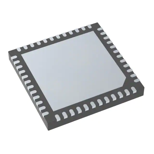
UFQFPN32 package information
UFQFPN32 is a 32-pin, 5x5 mm, 0.5 mm pitch ultra-thin fine-pitch quad flat package.
108/122
DocID022265 Rev 7
�STM32F051x4 STM32F051x6 STM32F051x8
Package information
Figure 52. UFQFPN32 package outline
'
$
H
$�
$�
'�
GGG &
&
6($7,1*
3/$1(
E
H
(�
E
(� (
�
/
��
3,1���,GHQWLILHU
'�
/
$�%�B0(B9�
1. Drawing is not to scale.
2. All leads/pads should also be soldered to the PCB to improve the lead/pad solder joint life.
3. There is an exposed die pad on the underside of the UFQFPN package. This pad is used for the device
ground and must be connected. It is referred to as pin 0 in Table: Pin definitions.
DocID022265 Rev 7
109/122
115
�Package information
STM32F051x4 STM32F051x6 STM32F051x8
Table 73. UFQFPN32 package mechanical data
inches(1)
millimeters
Symbol
Min
Typ
Max
Min
Typ
Max
A
0.500
0.550
0.600
0.0197
0.0217
0.0236
A1
0.000
0.020
0.050
0.0000
0.0008
0.0020
A3
-
0.152
-
-
0.0060
-
b
0.180
0.230
0.280
0.0071
0.0091
0.0110
D
4.900
5.000
5.100
0.1929
0.1969
0.2008
D1
3.400
3.500
3.600
0.1339
0.1378
0.1417
D2
3.400
3.500
3.600
0.1339
0.1378
0.1417
E
4.900
5.000
5.100
0.1929
0.1969
0.2008
E1
3.400
3.500
3.600
0.1339
0.1378
0.1417
E2
3.400
3.500
3.600
0.1339
0.1378
0.1417
e
-
0.500
-
-
0.0197
-
L
0.300
0.400
0.500
0.0118
0.0157
0.0197
ddd
-
-
0.080
-
-
0.0031
1. Values in inches are converted from mm and rounded to 4 decimal digits.
Figure 53. Recommended footprint for UFQFPN32 package
����
����
��
��
�
����
��
����
����
����
����
����
����
�
��
��
�
����
1. Dimensions are expressed in millimeters.
110/122
DocID022265 Rev 7
����
$�%�B)3B9�
�STM32F051x4 STM32F051x6 STM32F051x8
Package information
Device marking
The following figure gives an example of topside marking orientation versus pin 1 identifier
location.
Other optional marking or inset/upset marks, which identify the parts throughout supply
chain operations, are not indicated below.
Figure 54. UFQFPN32 package marking example
3URGXFW�LGHQWLILFDWLRQ����
)���.��
'DWH�FRGH
<
::
5HYLVLRQ�FRGH
5
'RW��SLQ�����
06Y�����9�
1. Parts marked as "ES", "E" or accompanied by an Engineering Sample notification letter, are not yet
qualified and therefore not yet ready to be used in production and any consequences deriving from such
usage will not be at ST charge. In no event, ST will be liable for any customer usage of these engineering
samples in production. ST Quality has to be contacted prior to any decision to use these Engineering
Samples to run qualification activity.
DocID022265 Rev 7
111/122
115
�Package information
7.8
STM32F051x4 STM32F051x6 STM32F051x8
Thermal characteristics
The maximum chip junction temperature (TJmax) must never exceed the values given in
Table 20: General operating conditions.
The maximum chip-junction temperature, TJ max, in degrees Celsius, may be calculated
using the following equation:
TJ max = TA max + (PD max x ΘJA)
Where:
•
TA max is the maximum ambient temperature in °C,
•
ΘJA is the package junction-to-ambient thermal resistance, in °C/W,
•
PD max is the sum of PINT max and PI/O max (PD max = PINT max + PI/Omax),
•
PINT max is the product of IDD and VDD, expressed in Watts. This is the maximum chip
internal power.
PI/O max represents the maximum power dissipation on output pins where:
PI/O max = Σ (VOL × IOL) + Σ ((VDDIOx – VOH) × IOH),
taking into account the actual VOL / IOL and VOH / IOH of the I/Os at low and high level in the
application.
Table 74. Package thermal characteristics
Symbol
ΘJA
7.8.1
Parameter
Value
Thermal resistance junction-ambient
LQFP64 - 10 × 10 mm / 0.5 mm pitch
45
Thermal resistance junction-ambient
LQFP48 - 7 × 7 mm
55
Thermal resistance junction-ambient
LQFP32 - 7 × 7 mm
56
Thermal resistance junction-ambient
UFBGA64 - 5 × 5 mm
65
Thermal resistance junction-ambient
UFQFPN48 - 7 × 7 mm
32
Thermal resistance junction-ambient
UFQFPN32 - 5 × 5 mm
38
Thermal resistance junction-ambient
WLCSP36 - 2.6 × 2.7 mm
60
Unit
°C/W
Reference document
JESD51-2 Integrated Circuits Thermal Test Method Environment Conditions - Natural
Convection (Still Air). Available from www.jedec.org
7.8.2
Selecting the product temperature range
When ordering the microcontroller, the temperature range is specified in the ordering
information scheme shown in Section 8: Ordering information.
112/122
DocID022265 Rev 7
�STM32F051x4 STM32F051x6 STM32F051x8
Package information
Each temperature range suffix corresponds to a specific guaranteed ambient temperature at
maximum dissipation and, to a specific maximum junction temperature.
As applications do not commonly use the STM32F051xx at maximum dissipation, it is useful
to calculate the exact power consumption and junction temperature to determine which
temperature range will be best suited to the application.
The following examples show how to calculate the temperature range needed for a given
application.
Example 1: High-performance application
Assuming the following application conditions:
Maximum ambient temperature TAmax = 82 °C (measured according to JESD51-2),
IDDmax = 50 mA, VDD = 3.5 V, maximum 20 I/Os used at the same time in output at low
level with IOL = 8 mA, VOL= 0.4 V and maximum 8 I/Os used at the same time in output
at low level with IOL = 20 mA, VOL= 1.3 V
PINTmax = 50 mA × 3.5 V= 175 mW
PIOmax = 20 × 8 mA × 0.4 V + 8 × 20 mA × 1.3 V = 272 mW
This gives: PINTmax = 175 mW and PIOmax = 272 mW:
PDmax = 175 + 272 = 447 mW
Using the values obtained in Table 74 TJmax is calculated as follows:
–
For LQFP64, 45 °C/W
TJmax = 82 °C + (45 °C/W × 447 mW) = 82 °C + 20.115 °C = 102.115 °C
This is within the range of the suffix 6 version parts (–40 < TJ < 105 °C) see Table 20:
General operating conditions.
In this case, parts must be ordered at least with the temperature range suffix 6 (see
Section 8: Ordering information).
Note:
With this given PDmax we can find the TAmax allowed for a given device temperature range
(order code suffix 6 or 7).
Suffix 6: TAmax = TJmax - (45°C/W × 447 mW) = 105-20.115 = 84.885 °C
Suffix 7: TAmax = TJmax - (45°C/W × 447 mW) = 125-20.115 = 104.885 °C
Example 2: High-temperature application
Using the same rules, it is possible to address applications that run at high ambient
temperatures with a low dissipation, as long as junction temperature TJ remains within the
specified range.
Assuming the following application conditions:
Maximum ambient temperature TAmax = 100 °C (measured according to JESD51-2),
IDDmax = 20 mA, VDD = 3.5 V, maximum 20 I/Os used at the same time in output at low
level with IOL = 8 mA, VOL= 0.4 V
PINTmax = 20 mA × 3.5 V= 70 mW
PIOmax = 20 × 8 mA × 0.4 V = 64 mW
This gives: PINTmax = 70 mW and PIOmax = 64 mW:
PDmax = 70 + 64 = 134 mW
Thus: PDmax = 134 mW
DocID022265 Rev 7
113/122
115
�Package information
STM32F051x4 STM32F051x6 STM32F051x8
Using the values obtained in Table 74 TJmax is calculated as follows:
–
For LQFP64, 45 °C/W
TJmax = 100 °C + (45 °C/W × 134 mW) = 100 °C + 6.03 °C = 106.03 °C
This is above the range of the suffix 6 version parts (–40 < TJ < 105 °C).
In this case, parts must be ordered at least with the temperature range suffix 7 (see
Section 8: Ordering information) unless we reduce the power dissipation in order to be able
to use suffix 6 parts.
Refer to Figure 55 to select the required temperature range (suffix 6 or 7) according to your
ambient temperature or power requirements.
Figure 55. LQFP64 PD max versus TA
���
3'��P:�
���
���
���
6XIIL[��
���
6XIIL[��
���
���
�
��
��
��
��
���
���
7$��&�
114/122
DocID022265 Rev 7
���
���
06Y�����9�
�STM32F051x4 STM32F051x6 STM32F051x8
8
Ordering information
Ordering information
For a list of available options (memory, package, and so on) or for further information on any
aspect of this device, please contact your nearest ST sales office.
Table 75. Ordering information scheme
STM32
Example:
F
051
R
8
T
6
x
Device family
STM32 = ARM-based 32-bit microcontroller
Product type
F = General-purpose
Sub-family
051 = STM32F051xx
Pin count
K = 32 pins
T = 36 pins
C = 48 pins
R = 64 pins
User code memory size
4 = 16 Kbyte
6 = 32 Kbyte
8 = 64 Kbyte
Package
H = UFBGA
T = LQFP
U = UFQFPN
Y = WLCSP
Temperature range
6 = –40 °C to +85 °C
7 = –40 °C to +105 °C
Options
xxx = code ID of programmed parts (includes packing type)
TR = tape and reel packing
blank = tray packing
DocID022265 Rev 7
115/122
115
�Revision history
9
STM32F051x4 STM32F051x6 STM32F051x8
Revision history
Table 76. Document revision history
Date
Revision
05-Apr-2012
1
Initial release
2
Updated Table: STM32F051xx family device features and
peripheral counts for SPI and I2C in 32-pin package.
Corrected Group 3 pin order in Table: Capacitive sensing GPIOs
available on STM32F051xx devices.
Updated the current consumption values in Section: Electrical
characteristics.
Updated Table: HSI14 oscillator characteristics
3
Features reorganized and Figure: Block diagram structure
changed.
Added LQFP32 package.
Updated Section: Cyclic redundancy check calculation unit
(CRC).
Modified the number of priority levels in Section: Nested
vectored interrupt controller (NVIC).
Added note 3. for PB2 and PB8, changed TIM2_CH_ETR into
TIM2_CH1_ETR in Table: Pin definitions and Table: Alternate
functions selected through GPIOA_AFR registers for port A.
Added Table: Alternate functions selected through GPIOB_AFR
registers for port B.
Updated IVDD, IVSS, and IINJ(PIN) in Table: Current
characteristics.
Updated ACCHSI in Table: HSI oscillator characteristics and
Table: HSI14 oscillator characteristics.
Updated Table: I/O current injection susceptibility.
Added BOOT0 input low and high level voltage in Table: I/O
static characteristics.
Modified number of pins in VOL and VOH description, and
changed condition for VOLFM+ in Table: Output voltage
characteristics.
Changed VDD to VDDA in Figure: Typical connection diagram
using the ADC.
Updated Ts_temp in Table: TS characteristics.
Updated Figure: I/O AC characteristics definition.
25-Apr-2012
23-Jul-2012
116/122
Changes
DocID022265 Rev 7
�STM32F051x4 STM32F051x6 STM32F051x8
Revision history
Table 76. Document revision history (continued)
Date
13-Jan-2014
Revision
Changes
4
Modified datasheet title.
Added packages UFQFPN48 and UFBGA64.
Replaced “backup domain with “RTC domain” throughout the
document.
Changed SRAM value from “4 to 8 Kbyte” to “8 Kbyte”
Replaced IWWDG with IWDG in Figure: Block diagram.
Added inputs LSI and LSE to the multiplexer in Figure: Clock
tree.
Added feature “Reference clock detection” in Section: Real-time
clock (RTC) and backup registers.
Modified junction temperature in Table: Thermal characteristics.
Renamed Table: Internal voltage reference calibration values.
Replaced VDD with VDDA and VRERINT with ΔVREFINT in Table:
Embedded internal reference voltage.
Rephrased introduction of Section: Touch sensing controller
(TSC).
Rephrased Section: Voltage regulator.
Added sentence “If this is used when the voltage regulator is put
in low power mode...” under “Stop mode” in Section: Low-power
modes.
Removed sentence “The internal voltage reference is also
connected to ADC_IN17 input channel of the ADC.” in Section:
Comparators (COMP).
Removed feature “Periodic wakeup from Stop/Standby” in
Section: Real-time clock (RTC) and backup registers.
Replaced IDD with IDDA in Table: HSI oscillator characteristics,
Table: HSI14 oscillator characteristics and Table: LSI oscillator
characteristics.
Moved section “Wakeup time from low-power mode” to
Section 6.3.6 and rephrased the section.
Added lines D2 and E2 in Table: UFQFPN48 – 7 x 7 mm, 0.5
mm pitch, package mechanical data.
Added “The peripheral clock used is 48 MHz.” in Section Onchip peripheral current consumption.
DocID022265 Rev 7
117/122
121
�Revision history
STM32F051x4 STM32F051x6 STM32F051x8
Table 76. Document revision history (continued)
Date
13-Jan-2014
118/122
Revision
Changes
4
(continued)
Added “Negative induced leakage current is caused by negative
injection and positive induced leakage current is caused by
positive injection” in Section Functional susceptibility to I/O
current injection.
Replaced reference "JESD22-C101" with "ANSI/ESD
STM5.3.1" in Table : ESD absolute maximum ratings.
Merged Table: Typical and maximum VDD consumption in Stop
and Standby modes and Table: Typical and maximum VDDA
consumption in Stop and Standby modes into Table: Typical and
maximum current consumption in Stop and Standby modes.
Updated:
– Table: Temperature sensor calibration values,
– Table: Internal voltage reference calibration values,
– Table: Current characteristics,
– Table: General operating conditions,
– Table: Typical and maximum current consumption from the
VDDA supply,
– Table: Low-power mode wakeup timings,
– Table: I/O current injection susceptibility,
– Table: I/O static characteristics,
– Table: Output voltage characteristics,
– Table: NRST pin characteristics,
– Table: I2C analog filter characteristics,
– Figure: Power supply scheme,
– Figure: TC and TTa I/O input characteristics,
– Figure: Five volt tolerant (FT and FTf) I/O input
characteristics,
– Figure: I/O AC characteristics definition,
– Figure: ADC accuracy characteristics,
– Figure: Typical connection diagram using the ADC,
– Figure: LQFP64 – 10 x 10 mm 64 pin low-profile quad flat
package outline,
– Figure: LQFP64 recommended footprint,
– Figure: LQFP48 – 7 x 7 mm, 48 pin low-profile quad flat
package outline,
– Figure: LQFP48 recommended footprint,
– Figure: LQFP32 – 7 x 7 mm 32-pin low-profile quad flat
package outline,
– Figure: LQFP32 recommended footprint,
– Figure: UFQFPN48 – 7 x 7 mm, 0.5 mm pitch, package
outline.
DocID022265 Rev 7
�STM32F051x4 STM32F051x6 STM32F051x8
Revision history
Table 76. Document revision history (continued)
Date
28-Aug-2015
Revision
5
Changes
Updated the following:
– DAC and power management feature descriptions in Features
– Table 2: STM32F051xx family device features and peripheral
count
– Section 3.5.1: Power supply schemes
– Figure 13: Power supply scheme
– Table 17: Voltage characteristics
– Table 20: General operating conditions: updated the footnote
for VIN parameter
– Table 28: Typical and maximum current consumption from the
VBAT supply
– Table 52: ADC characteristics
– Table 33: High-speed external user clock characteristics:
replaced VDD with VDDIOX
– Table 34: Low-speed external user clock characteristics:
replaced VDD with VDDIOX
– Table 37: HSI oscillator characteristics and Figure 19: HSI
oscillator accuracy characterization results for soldered parts
– Table 38: HSI14 oscillator characteristics: changed the min
value for ACCHSI14
– Table 41: Flash memory characteristics: changed the values
for tME and IDD in write mode
– Table 43: EMS characteristics: changed the value of VEFTB
– Table 45: ESD absolute maximum ratings
– Figure 10: STM32F051x8 memory map
– Figure 21: TC and TTa I/O input characteristics
– Figure 22: Five volt tolerant (FT and FTf) I/O input
characteristics
– Figure 23: I/O AC characteristics definition
– tSTART definition in Table 24: Embedded internal reference
voltage
– tSTAB characteristics in Table 52: ADC characteristics
– Table 56: Comparator characteristics: changed the
description and values for VSC, VDDA and VREFINT
parameters. Added Figure 28: Maximum VREFINT scaler
startup time from power down
– Table 57: TS characteristics: changed the min value for TStemp
– Table 58: VBAT monitoring characteristics: changed the min
value for TS-vbat and the typical value for R parameters
– Section 6.3.22: Communication interfaces: updated the
description and features in the subsection I2C interface
characteristics
– Table 64: I2S characteristics: updated the min values for data
input hold time (master and slave receiver)
DocID022265 Rev 7
119/122
121
�Revision history
STM32F051x4 STM32F051x6 STM32F051x8
Table 76. Document revision history (continued)
Date
28-Aug-2015
16-Dec-2015
120/122
Revision
Changes
5
(continued)
– Table 31: Peripheral current consumption
Addition of WLCSP36 package. Updates in:
– Section 2: Description
– Table 2: STM32F051xx family device features and peripheral
count
– Section 4: Pinouts and pin descriptions with the addition of
Figure 7: WLCSP36 package pinout
– Table 13: Pin definitions
– Table 20: General operating conditions
– Section 7: Package information with the addition of
Section 7.5: WLCSP36 package information
– Table 74: Package thermal characteristics
– Section 8: Part numbering
Update of the device marking examples in Section 7: Package
information.
6
Section 2: Description:
– Table 2: STM32F051xx family device features and peripheral
count - number of SPIs corrected for 64-pin packages
– Figure 1: Block diagram modified
Section 3: Functional overview:
– Figure 2: Clock tree modified; divider for CEC corrected
– Table 8: Comparison of I2C analog and digital filters - adding
20 mA information for FastPlus mode
Section 4: Pinouts and pin descriptions:
– Package pinout figures updated (look and feel)
– Figure 7: WLCSP36 package pinout - now presented in top
view
– Table 13: Pin definitions - notes added (VSSA corrected to pin
16 on LQFP32); note 5 added
Section 5: Memory mapping:
– added information on STM32F051x4/x6 difference versus
STM32F051x8 map in Figure 10
Section 6: Electrical characteristics:
– Table 24: Embedded internal reference voltage - removed 40°C-85°C temperature range line and the associated note
– Table 48: I/O static characteristics - removed note
– Section 6.3.16: 12-bit ADC characteristics - changed
introductory sentence
– Table 52: ADC characteristics updated and table footnotes 3
and 4 added
– Table 56: Comparator characteristics - VDDA min modified
– Table 59: TIMx characteristics modified
– Table 64: I2S characteristics reorganized
– Figure 52: UFQFPN32 package outline - figure footnotes
added
DocID022265 Rev 7
�STM32F051x4 STM32F051x6 STM32F051x8
Revision history
Table 76. Document revision history (continued)
Date
06-Jan-2017
Revision
Changes
7
Section 6: Electrical characteristics:
– Table 36: LSE oscillator characteristics (fLSE = 32.768 kHz) information on configuring different drive capabilities
removed. See the corresponding reference manual.
– Table 24: Embedded internal reference voltage - VREFINT
values
– Table 55: DAC characteristics - min. RLOAD to VDDA defined
– Figure 29: SPI timing diagram - slave mode and CPHA = 0
and Figure 30: SPI timing diagram - slave mode and CPHA =
1 enhanced and corrected
Section 8: Ordering information:
– The name of the section changed from the previous “Part
numbering”
DocID022265 Rev 7
121/122
121
�STM32F051x4 STM32F051x6 STM32F051x8
IMPORTANT NOTICE – PLEASE READ CAREFULLY
STMicroelectronics NV and its subsidiaries (“ST”) reserve the right to make changes, corrections, enhancements, modifications, and
improvements to ST products and/or to this document at any time without notice. Purchasers should obtain the latest relevant information on
ST products before placing orders. ST products are sold pursuant to ST’s terms and conditions of sale in place at the time of order
acknowledgement.
Purchasers are solely responsible for the choice, selection, and use of ST products and ST assumes no liability for application assistance or
the design of Purchasers’ products.
No license, express or implied, to any intellectual property right is granted by ST herein.
Resale of ST products with provisions different from the information set forth herein shall void any warranty granted by ST for such product.
ST and the ST logo are trademarks of ST. All other product or service names are the property of their respective owners.
Information in this document supersedes and replaces information previously supplied in any prior versions of this document.
© 2017 STMicroelectronics – All rights reserved
122/122
DocID022265 Rev 7
�