STM32F398VE
ARM® Cortex®-M4 32b MCU+FPU, up to 512KB Flash, 80KB
SRAM, FSMC, 4 ADCs, 2 DAC ch., 7 comp, 4 Op-Amp, 1.8 V
Datasheet - production data
Features
Core: ARM® Cortex®-M4 32-bit CPU with
72 MHz FPU, single-cycle multiplication and
HW division, DSP instruction and MPU
(memory protection unit)
Memories
– Up to 512 Kbytes of Flash memory
– 64 Kbytes of SRAM, with HW parity check
implemented on the first 32 Kbytes.
– Routine booster: 16 Kbytes of SRAM on
instruction and data bus, with HW parity
check (CCM)
– Flexible memory controller (FSMC) for static
memories, with four Chip Select
CRC calculation unit
Reset and supply management
– Low power modes: Sleep and Stop
– Supply: VDD = 1.8 V ± 8%
VDDA voltage range = 1.65 V to 3.6 V
– VBAT supply for RTC and backup registers
Clock management
– 4 to 32 MHz crystal oscillator
– 32 kHz oscillator for RTC with calibration
– Internal 8 MHz RC with x 16 PLL option
– Internal 40 kHz oscillator
Up to 85 fast I/Os
– All mappable on external interrupt vectors
– Several 5 V-tolerant
Interconnect matrix
12-channel DMA controller
Four ADCs 0.20 µs (up to 38 channels) with
selectable resolution of 12/10/8/6 bits, 0 to
3.6 V conversion range, separate analog
supply from 1.8 to 3.6 V
Two 12-bit DAC channels with analog supply
from 2.4 to 3.6 V
Seven ultra-fast rail-to-rail analog comparators
with analog supply from 1.8 to 3.6 V
Four operational amplifiers that can be used in
PGA mode, all terminals accessible with analog
supply from 2.4 to 3.6 V
Up to 24 capacitive sensing channels supporting
touchkey, linear and rotary touch sensors
Up to 14 timers
July 2015
This is information on a product in full production.
LQFP100
(14 mm × 14 mm)
– One 32-bit timer and two 16-bit timers with
up to four IC/OC/PWM or pulse counter and
quadrature (incremental) encoder input
– Three 16-bit 6-channel advanced-control
timers, with up to six PWM channels,
deadtime generation and emergency stop
– One 16-bit timer with two IC/OCs, one
OCN/PWM, deadtime generation and
emergency stop
– Two 16-bit timers with IC/OC/OCN/PWM,
deadtime generation and emergency stop
– Two watchdog timers (independent, window)
– One SysTick timer: 24-bit downcounter
– Two 16-bit basic timers to drive the DAC
Calendar RTC with Alarm, periodic wakeup
from Stop/Standby
Communication interfaces
– CAN interface (2.0B Active)
– Three I2C Fast mode plus (1 Mbit/s) with
20 mA current sink, SMBus/PMBus, wakeup
from STOP
– Up to five USART/UARTs (ISO 7816
interface, LIN, IrDA, modem control)
– Up to four SPIs, 4 to 16 programmable bit
frames, two with multiplexed half/full duplex
I2S interface
– Infrared transmitter
SWD, Cortex®-M4 with FPU ETM, JTAG
96-bit unique ID
DocID027227 Rev 2
1/151
www.st.com
�Contents
STM32F398VE
Contents
1
Introduction . . . . . . . . . . . . . . . . . . . . . . . . . . . . . . . . . . . . . . . . . . . . . . . . 9
2
Description . . . . . . . . . . . . . . . . . . . . . . . . . . . . . . . . . . . . . . . . . . . . . . . . 10
3
Functional overview . . . . . . . . . . . . . . . . . . . . . . . . . . . . . . . . . . . . . . . . 13
3.1
ARM® Cortex®-M4 core with FPU with embedded Flash and SRAM . . . 13
3.2
Memory protection unit (MPU) . . . . . . . . . . . . . . . . . . . . . . . . . . . . . . . . . 13
3.3
Embedded Flash memory . . . . . . . . . . . . . . . . . . . . . . . . . . . . . . . . . . . . 13
3.4
Embedded SRAM . . . . . . . . . . . . . . . . . . . . . . . . . . . . . . . . . . . . . . . . . . . 13
3.5
Boot modes . . . . . . . . . . . . . . . . . . . . . . . . . . . . . . . . . . . . . . . . . . . . . . . 14
3.6
Cyclic redundancy check (CRC) . . . . . . . . . . . . . . . . . . . . . . . . . . . . . . . 14
3.7
Power management . . . . . . . . . . . . . . . . . . . . . . . . . . . . . . . . . . . . . . . . . 15
3.7.1
Power supply schemes . . . . . . . . . . . . . . . . . . . . . . . . . . . . . . . . . . . . . 15
3.7.2
Power supply supervisor . . . . . . . . . . . . . . . . . . . . . . . . . . . . . . . . . . . . 15
3.7.3
Low-power modes . . . . . . . . . . . . . . . . . . . . . . . . . . . . . . . . . . . . . . . . . 15
3.8
Interconnect matrix . . . . . . . . . . . . . . . . . . . . . . . . . . . . . . . . . . . . . . . . . . 16
3.9
Clocks and startup . . . . . . . . . . . . . . . . . . . . . . . . . . . . . . . . . . . . . . . . . . 16
3.10
General-purpose input/outputs (GPIOs) . . . . . . . . . . . . . . . . . . . . . . . . . . 18
3.11
Direct memory access (DMA) . . . . . . . . . . . . . . . . . . . . . . . . . . . . . . . . . 18
3.12
Flexible static memory controller (FSMC) . . . . . . . . . . . . . . . . . . . . . . . . 18
3.13
Interrupts and events . . . . . . . . . . . . . . . . . . . . . . . . . . . . . . . . . . . . . . . . 19
3.13.1
3.14
Fast analog-to-digital converter (ADC) . . . . . . . . . . . . . . . . . . . . . . . . . . . 19
3.14.1
Temperature sensor . . . . . . . . . . . . . . . . . . . . . . . . . . . . . . . . . . . . . . . . 20
3.14.2
Internal voltage reference (VREFINT) . . . . . . . . . . . . . . . . . . . . . . . . . . . 20
3.14.3
VBAT battery voltage monitoring . . . . . . . . . . . . . . . . . . . . . . . . . . . . . . . 20
3.14.4
OPAMP reference voltage (VREFOPAMP) . . . . . . . . . . . . . . . . . . . . . . 20
3.15
Digital-to-analog converter (DAC) . . . . . . . . . . . . . . . . . . . . . . . . . . . . . . 21
3.16
Operational amplifier (OPAMP) . . . . . . . . . . . . . . . . . . . . . . . . . . . . . . . . 21
3.17
Ultra-fast comparators (COMP) . . . . . . . . . . . . . . . . . . . . . . . . . . . . . . . . 21
3.18
Timers and watchdogs . . . . . . . . . . . . . . . . . . . . . . . . . . . . . . . . . . . . . . . 22
3.18.1
2/151
Nested vectored interrupt controller (NVIC) . . . . . . . . . . . . . . . . . . . . . . 19
Advanced timers (TIM1, TIM8, TIM20) . . . . . . . . . . . . . . . . . . . . . . . . . 23
DocID027227 Rev 2
�STM32F398VE
Contents
3.18.2
General-purpose timers (TIM2, TIM3, TIM4, TIM15, TIM16, TIM17) . . 23
3.18.3
Basic timers (TIM6, TIM7) . . . . . . . . . . . . . . . . . . . . . . . . . . . . . . . . . . . 23
3.18.4
Independent watchdog (IWDG) . . . . . . . . . . . . . . . . . . . . . . . . . . . . . . . 24
3.18.5
Window watchdog (WWDG) . . . . . . . . . . . . . . . . . . . . . . . . . . . . . . . . . 24
3.18.6
SysTick timer . . . . . . . . . . . . . . . . . . . . . . . . . . . . . . . . . . . . . . . . . . . . . 24
3.19
Real-time clock (RTC) and backup registers . . . . . . . . . . . . . . . . . . . . . . 24
3.20
Inter-integrated circuit interface (I2C) . . . . . . . . . . . . . . . . . . . . . . . . . . . . 25
3.21
Universal synchronous/asynchronous receiver transmitter (USART) . . . 26
3.22
Universal asynchronous receiver transmitter (UART) . . . . . . . . . . . . . . . 27
3.23
Serial peripheral interface (SPI)/Inter-integrated sound interfaces (I2S) . 28
3.24
Controller area network (CAN) . . . . . . . . . . . . . . . . . . . . . . . . . . . . . . . . . 28
3.25
Infrared Transmitter . . . . . . . . . . . . . . . . . . . . . . . . . . . . . . . . . . . . . . . . . 29
3.26
Touch sensing controller (TSC) . . . . . . . . . . . . . . . . . . . . . . . . . . . . . . . . 29
3.27
Development support . . . . . . . . . . . . . . . . . . . . . . . . . . . . . . . . . . . . . . . . 31
3.27.1
Serial wire JTAG debug port (SWJ-DP) . . . . . . . . . . . . . . . . . . . . . . . . . 31
3.27.2
Embedded trace macrocell™ . . . . . . . . . . . . . . . . . . . . . . . . . . . . . . . . 31
4
Pinouts and pin description . . . . . . . . . . . . . . . . . . . . . . . . . . . . . . . . . . 32
5
Memory mapping . . . . . . . . . . . . . . . . . . . . . . . . . . . . . . . . . . . . . . . . . . . 52
6
Electrical characteristics . . . . . . . . . . . . . . . . . . . . . . . . . . . . . . . . . . . . 56
6.1
Parameter conditions . . . . . . . . . . . . . . . . . . . . . . . . . . . . . . . . . . . . . . . . 56
6.1.1
Minimum and maximum values . . . . . . . . . . . . . . . . . . . . . . . . . . . . . . . 56
6.1.2
Typical values . . . . . . . . . . . . . . . . . . . . . . . . . . . . . . . . . . . . . . . . . . . . 56
6.1.3
Typical curves . . . . . . . . . . . . . . . . . . . . . . . . . . . . . . . . . . . . . . . . . . . . 56
6.1.4
Loading capacitor . . . . . . . . . . . . . . . . . . . . . . . . . . . . . . . . . . . . . . . . . 56
6.1.5
Pin input voltage . . . . . . . . . . . . . . . . . . . . . . . . . . . . . . . . . . . . . . . . . . 56
6.1.6
Power supply scheme . . . . . . . . . . . . . . . . . . . . . . . . . . . . . . . . . . . . . . 57
6.1.7
Current consumption measurement . . . . . . . . . . . . . . . . . . . . . . . . . . . 58
6.2
Absolute maximum ratings . . . . . . . . . . . . . . . . . . . . . . . . . . . . . . . . . . . . 59
6.3
Operating conditions . . . . . . . . . . . . . . . . . . . . . . . . . . . . . . . . . . . . . . . . 61
6.3.1
General operating conditions . . . . . . . . . . . . . . . . . . . . . . . . . . . . . . . . . 61
6.3.2
Operating conditions at power-up / power-down . . . . . . . . . . . . . . . . . . 62
6.3.3
Embedded reference voltage . . . . . . . . . . . . . . . . . . . . . . . . . . . . . . . . . 63
6.3.4
Supply current characteristics . . . . . . . . . . . . . . . . . . . . . . . . . . . . . . . . 63
DocID027227 Rev 2
3/151
4
�Contents
7
STM32F398VE
6.3.5
Wakeup time from low-power mode . . . . . . . . . . . . . . . . . . . . . . . . . . . 76
6.3.6
External clock source characteristics . . . . . . . . . . . . . . . . . . . . . . . . . . . 77
6.3.7
Internal clock source characteristics . . . . . . . . . . . . . . . . . . . . . . . . . . . 83
6.3.8
PLL characteristics . . . . . . . . . . . . . . . . . . . . . . . . . . . . . . . . . . . . . . . . 84
6.3.9
Memory characteristics . . . . . . . . . . . . . . . . . . . . . . . . . . . . . . . . . . . . . 85
6.3.10
FSMC characteristics . . . . . . . . . . . . . . . . . . . . . . . . . . . . . . . . . . . . . . . 85
6.3.11
EMC characteristics . . . . . . . . . . . . . . . . . . . . . . . . . . . . . . . . . . . . . . . 109
6.3.12
Electrical sensitivity characteristics . . . . . . . . . . . . . . . . . . . . . . . . . . . 110
6.3.13
I/O current injection characteristics . . . . . . . . . . . . . . . . . . . . . . . . . . . 111
6.3.14
I/O port characteristics . . . . . . . . . . . . . . . . . . . . . . . . . . . . . . . . . . . . . 113
6.3.15
NRST pin characteristics . . . . . . . . . . . . . . . . . . . . . . . . . . . . . . . . . . . 117
6.3.16
NPOR pin characteristics . . . . . . . . . . . . . . . . . . . . . . . . . . . . . . . . . . . 118
6.3.17
Timer characteristics . . . . . . . . . . . . . . . . . . . . . . . . . . . . . . . . . . . . . . 119
6.3.18
Communications interfaces . . . . . . . . . . . . . . . . . . . . . . . . . . . . . . . . . 121
6.3.19
ADC characteristics . . . . . . . . . . . . . . . . . . . . . . . . . . . . . . . . . . . . . . . 127
6.3.20
DAC electrical specifications . . . . . . . . . . . . . . . . . . . . . . . . . . . . . . . . 136
6.3.21
Comparator characteristics . . . . . . . . . . . . . . . . . . . . . . . . . . . . . . . . . 137
6.3.22
Operational amplifier characteristics . . . . . . . . . . . . . . . . . . . . . . . . . . 139
6.3.23
Temperature sensor characteristics . . . . . . . . . . . . . . . . . . . . . . . . . . . 142
6.3.24
VBAT monitoring characteristics . . . . . . . . . . . . . . . . . . . . . . . . . . . . . . 142
Package information . . . . . . . . . . . . . . . . . . . . . . . . . . . . . . . . . . . . . . . 143
7.1
LQFP100 package information . . . . . . . . . . . . . . . . . . . . . . . . . . . . . . . . 143
7.2
Thermal characteristics . . . . . . . . . . . . . . . . . . . . . . . . . . . . . . . . . . . . . 146
7.2.1
Reference document . . . . . . . . . . . . . . . . . . . . . . . . . . . . . . . . . . . . . . 146
7.2.2
Selecting the product temperature range . . . . . . . . . . . . . . . . . . . . . . 146
8
Part numbering . . . . . . . . . . . . . . . . . . . . . . . . . . . . . . . . . . . . . . . . . . . 149
9
Revision history . . . . . . . . . . . . . . . . . . . . . . . . . . . . . . . . . . . . . . . . . . 150
4/151
DocID027227 Rev 2
�STM32F398VE
List of tables
List of tables
Table 1.
Table 2.
Table 3.
Table 4.
Table 5.
Table 6.
Table 7.
Table 8.
Table 9.
Table 10.
Table 11.
Table 12.
Table 13.
Table 14.
Table 15.
Table 16.
Table 17.
Table 18.
Table 19.
Table 20.
Table 21.
Table 22.
Table 23.
Table 24.
Table 25.
Table 26.
Table 27.
Table 28.
Table 29.
Table 30.
Table 31.
Table 32.
Table 33.
Table 34.
Table 35.
Table 36.
Table 37.
Table 38.
Table 39.
Table 40.
Table 41.
Table 42.
Table 43.
Table 44.
Table 45.
Table 46.
STM32F398VE device features and peripheral counts . . . . . . . . . . . . . . . . . . . . . . . . . . . 11
External analog supply values for analog peripherals . . . . . . . . . . . . . . . . . . . . . . . . . . . . 15
STM32F398VE peripheral interconnect matrix . . . . . . . . . . . . . . . . . . . . . . . . . . . . . . . . . . 16
Timer feature comparison . . . . . . . . . . . . . . . . . . . . . . . . . . . . . . . . . . . . . . . . . . . . . . . . . . 22
Comparison of I2C analog and digital filters . . . . . . . . . . . . . . . . . . . . . . . . . . . . . . . . . . . . 25
STM32F398VE I2C implementation . . . . . . . . . . . . . . . . . . . . . . . . . . . . . . . . . . . . . . . . . . 26
USART features . . . . . . . . . . . . . . . . . . . . . . . . . . . . . . . . . . . . . . . . . . . . . . . . . . . . . . . . . 27
STM32F398VE SPI/I2S implementation. . . . . . . . . . . . . . . . . . . . . . . . . . . . . . . . . . . . . . . 28
Capacitive sensing GPIOs available on STM32F398VE . . . . . . . . . . . . . . . . . . . . . . . . . . 30
Number of capacitive sensing channels available on
STM32F398VE . . . . . . . . . . . . . . . . . . . . . . . . . . . . . . . . . . . . . . . . . . . . . . . . . . . . . . . . . . 30
Legend/abbreviations used in the pinout table . . . . . . . . . . . . . . . . . . . . . . . . . . . . . . . . . . 33
STM32F398VE pin definitions . . . . . . . . . . . . . . . . . . . . . . . . . . . . . . . . . . . . . . . . . . . . . . 33
STM32F398VE alternate function mapping . . . . . . . . . . . . . . . . . . . . . . . . . . . . . . . . . . . . 41
Memory map, peripheral register boundary addresses . . . . . . . . . . . . . . . . . . . . . . . . . . . 53
Voltage characteristics . . . . . . . . . . . . . . . . . . . . . . . . . . . . . . . . . . . . . . . . . . . . . . . . . . . . 59
Current characteristics . . . . . . . . . . . . . . . . . . . . . . . . . . . . . . . . . . . . . . . . . . . . . . . . . . . . 60
Thermal characteristics. . . . . . . . . . . . . . . . . . . . . . . . . . . . . . . . . . . . . . . . . . . . . . . . . . . . 60
General operating conditions . . . . . . . . . . . . . . . . . . . . . . . . . . . . . . . . . . . . . . . . . . . . . . . 61
Operating conditions at power-up / power-down . . . . . . . . . . . . . . . . . . . . . . . . . . . . . . . . 62
Embedded internal reference voltage . . . . . . . . . . . . . . . . . . . . . . . . . . . . . . . . . . . . . . . . . 63
Internal reference voltage calibration values . . . . . . . . . . . . . . . . . . . . . . . . . . . . . . . . . . . 63
Typical and maximum current consumption from VDD supply at VDD = 1.8 V . . . . . . . . . . 65
Typical and maximum current consumption from the VDDA supply . . . . . . . . . . . . . . . . . . 66
Typical and maximum VDD consumption in Stop mode . . . . . . . . . . . . . . . . . . . . . . . . . . . 67
Typical and maximum VDDA consumption in Stop mode . . . . . . . . . . . . . . . . . . . . . . . . . . 67
Typical and maximum current consumption from VBAT supply. . . . . . . . . . . . . . . . . . . . . . 67
Typical current consumption in Run mode, code with data processing running
from Flash . . . . . . . . . . . . . . . . . . . . . . . . . . . . . . . . . . . . . . . . . . . . . . . . . . . . . . . . . . . . . 69
Typical current consumption in Sleep mode, code running from Flash or RAM . . . . . . . . . 70
Switching output I/O current consumption . . . . . . . . . . . . . . . . . . . . . . . . . . . . . . . . . . . . . 72
Peripheral current consumption . . . . . . . . . . . . . . . . . . . . . . . . . . . . . . . . . . . . . . . . . . . . . 74
Low-power mode wakeup timings . . . . . . . . . . . . . . . . . . . . . . . . . . . . . . . . . . . . . . . . . . . 76
High-speed external user clock characteristics. . . . . . . . . . . . . . . . . . . . . . . . . . . . . . . . . . 77
Low-speed external user clock characteristics . . . . . . . . . . . . . . . . . . . . . . . . . . . . . . . . . . 78
HSE oscillator characteristics . . . . . . . . . . . . . . . . . . . . . . . . . . . . . . . . . . . . . . . . . . . . . . . 79
LSE oscillator characteristics (fLSE = 32.768 kHz) . . . . . . . . . . . . . . . . . . . . . . . . . . . . . . . 81
HSI oscillator characteristics. . . . . . . . . . . . . . . . . . . . . . . . . . . . . . . . . . . . . . . . . . . . . . . . 83
LSI oscillator characteristics . . . . . . . . . . . . . . . . . . . . . . . . . . . . . . . . . . . . . . . . . . . . . . . . 84
PLL characteristics . . . . . . . . . . . . . . . . . . . . . . . . . . . . . . . . . . . . . . . . . . . . . . . . . . . . . . . 84
Flash memory characteristics . . . . . . . . . . . . . . . . . . . . . . . . . . . . . . . . . . . . . . . . . . . . . . . 85
Flash memory endurance and data retention . . . . . . . . . . . . . . . . . . . . . . . . . . . . . . . . . . . 85
Asynchronous non-multiplexed SRAM/PSRAM/NOR read timings . . . . . . . . . . . . . . . . . . 87
Asynchronous non-multiplexed SRAM/PSRAM/NOR read-NWAIT timings . . . . . . . . . . . . 87
Asynchronous non-multiplexed SRAM/PSRAM/NOR write timings . . . . . . . . . . . . . . . . . . 88
Asynchronous non-multiplexed SRAM/PSRAM/NOR write-NWAIT timings. . . . . . . . . . . . 89
Asynchronous multiplexed PSRAM/NOR read-NWAIT timings . . . . . . . . . . . . . . . . . . . . . 89
Asynchronous multiplexed PSRAM/NOR read timings. . . . . . . . . . . . . . . . . . . . . . . . . . . . 91
DocID027227 Rev 2
5/151
6
�List of tables
Table 47.
Table 48.
Table 49.
Table 50.
Table 51.
Table 52.
Table 53.
Table 54.
Table 55.
Table 56.
Table 57.
Table 58.
Table 59.
Table 60.
Table 61.
Table 62.
Table 63.
Table 64.
Table 65.
Table 66.
Table 67.
Table 68.
Table 69.
Table 70.
Table 71.
Table 72.
Table 73.
Table 74.
Table 75.
Table 76.
Table 77.
Table 78.
Table 79.
Table 80.
Table 81.
Table 82.
Table 83.
Table 84.
Table 85.
Table 86.
Table 87.
6/151
STM32F398VE
Asynchronous multiplexed PSRAM/NOR write timings . . . . . . . . . . . . . . . . . . . . . . . . . . . 93
Asynchronous multiplexed PSRAM/NOR write-NWAIT timings . . . . . . . . . . . . . . . . . . . . . 93
Synchronous multiplexed NOR/PSRAM read timings . . . . . . . . . . . . . . . . . . . . . . . . . . . . 95
Synchronous multiplexed PSRAM write timings . . . . . . . . . . . . . . . . . . . . . . . . . . . . . . . . 97
Synchronous non-multiplexed NOR/PSRAM read timings . . . . . . . . . . . . . . . . . . . . . . . . . 99
Synchronous non-multiplexed PSRAM write timings . . . . . . . . . . . . . . . . . . . . . . . . . . . . 101
Switching characteristics for PC Card/CF read and write cycles
in attribute/common space. . . . . . . . . . . . . . . . . . . . . . . . . . . . . . . . . . . . . . . . . . . . . . . . 102
Switching characteristics for PC Card/CF read and write cycles in I/O space . . . . . . . . . 105
Switching characteristics for NAND Flash read cycles . . . . . . . . . . . . . . . . . . . . . . . . . . 108
Switching characteristics for NAND Flash write cycles. . . . . . . . . . . . . . . . . . . . . . . . . . . 108
EMS characteristics . . . . . . . . . . . . . . . . . . . . . . . . . . . . . . . . . . . . . . . . . . . . . . . . . . . . . 109
EMI characteristics . . . . . . . . . . . . . . . . . . . . . . . . . . . . . . . . . . . . . . . . . . . . . . . . . . . . . . 110
ESD absolute maximum ratings . . . . . . . . . . . . . . . . . . . . . . . . . . . . . . . . . . . . . . . . . . . . 110
Electrical sensitivities . . . . . . . . . . . . . . . . . . . . . . . . . . . . . . . . . . . . . . . . . . . . . . . . . . . . 111
I/O current injection susceptibility . . . . . . . . . . . . . . . . . . . . . . . . . . . . . . . . . . . . . . . . . . . 112
I/O static characteristics . . . . . . . . . . . . . . . . . . . . . . . . . . . . . . . . . . . . . . . . . . . . . . . . . . 113
Output voltage characteristics . . . . . . . . . . . . . . . . . . . . . . . . . . . . . . . . . . . . . . . . . . . . . 115
I/O AC characteristics . . . . . . . . . . . . . . . . . . . . . . . . . . . . . . . . . . . . . . . . . . . . . . . . . . . . 116
NRST pin characteristics . . . . . . . . . . . . . . . . . . . . . . . . . . . . . . . . . . . . . . . . . . . . . . . . . 117
NPOR pin characteristics . . . . . . . . . . . . . . . . . . . . . . . . . . . . . . . . . . . . . . . . . . . . . . . . . 118
TIMx characteristics . . . . . . . . . . . . . . . . . . . . . . . . . . . . . . . . . . . . . . . . . . . . . . . . . . . . . 119
IWDG min/max timeout period at 40 kHz (LSI) . . . . . . . . . . . . . . . . . . . . . . . . . . . . . . . . 120
WWDG min-max timeout value @72 MHz (PCLK). . . . . . . . . . . . . . . . . . . . . . . . . . . . . . 120
I2C analog filter characteristics. . . . . . . . . . . . . . . . . . . . . . . . . . . . . . . . . . . . . . . . . . . . . 121
SPI characteristics . . . . . . . . . . . . . . . . . . . . . . . . . . . . . . . . . . . . . . . . . . . . . . . . . . . . . . 122
I2S characteristics . . . . . . . . . . . . . . . . . . . . . . . . . . . . . . . . . . . . . . . . . . . . . . . . . . . . . . . 124
ADC characteristics . . . . . . . . . . . . . . . . . . . . . . . . . . . . . . . . . . . . . . . . . . . . . . . . . . . . . 127
Maximum ADC RAIN . . . . . . . . . . . . . . . . . . . . . . . . . . . . . . . . . . . . . . . . . . . . . . . . . . . . 130
ADC accuracy - limited test conditions, 100-pin packages . . . . . . . . . . . . . . . . . . . . . . . 131
ADC accuracy, 100-pin packages- limited test conditions . . . . . . . . . . . . . . . . . . . . . . . . 133
ADC accuracy at 1MSPS . . . . . . . . . . . . . . . . . . . . . . . . . . . . . . . . . . . . . . . . . . . . . . . . . 134
DAC characteristics . . . . . . . . . . . . . . . . . . . . . . . . . . . . . . . . . . . . . . . . . . . . . . . . . . . . . 136
Comparator characteristics . . . . . . . . . . . . . . . . . . . . . . . . . . . . . . . . . . . . . . . . . . . . . . . . 137
Operational amplifier characteristics. . . . . . . . . . . . . . . . . . . . . . . . . . . . . . . . . . . . . . . . . 139
TS characteristics . . . . . . . . . . . . . . . . . . . . . . . . . . . . . . . . . . . . . . . . . . . . . . . . . . . . . . . 142
Temperature sensor calibration values. . . . . . . . . . . . . . . . . . . . . . . . . . . . . . . . . . . . . . . 142
VBAT monitoring characteristics . . . . . . . . . . . . . . . . . . . . . . . . . . . . . . . . . . . . . . . . . . . . 142
LQPF100 - 100-pin, 14 x 14 mm low-profile quad flat package
mechanical data . . . . . . . . . . . . . . . . . . . . . . . . . . . . . . . . . . . . . . . . . . . . . . . . . . . . . . . . 144
Package thermal characteristics . . . . . . . . . . . . . . . . . . . . . . . . . . . . . . . . . . . . . . . . . . . . 146
Ordering information scheme . . . . . . . . . . . . . . . . . . . . . . . . . . . . . . . . . . . . . . . . . . . . . . 149
Document revision history . . . . . . . . . . . . . . . . . . . . . . . . . . . . . . . . . . . . . . . . . . . . . . . . 150
DocID027227 Rev 2
�STM32F398VE
List of figures
List of figures
Figure 1.
Figure 2.
Figure 3.
Figure 4.
Figure 5.
Figure 6.
Figure 7.
Figure 8.
Figure 9.
Figure 10.
Figure 11.
Figure 12.
Figure 13.
Figure 14.
Figure 15.
Figure 16.
Figure 17.
Figure 18.
Figure 19.
Figure 20.
Figure 21.
Figure 22.
Figure 23.
Figure 24.
Figure 25.
Figure 26.
Figure 27.
Figure 28.
Figure 29.
Figure 30.
Figure 31.
Figure 32.
Figure 33.
Figure 34.
Figure 35.
Figure 36.
Figure 37.
Figure 38.
Figure 39.
Figure 40.
Figure 41.
Figure 42.
Figure 43.
Figure 44.
STM32F398VE block diagram . . . . . . . . . . . . . . . . . . . . . . . . . . . . . . . . . . . . . . . . . . . . . . 12
STM32F398VE clock tree . . . . . . . . . . . . . . . . . . . . . . . . . . . . . . . . . . . . . . . . . . . . . . . . . . 17
Infrared transmitter . . . . . . . . . . . . . . . . . . . . . . . . . . . . . . . . . . . . . . . . . . . . . . . . . . . . . . . 29
STM32F398VE LQFP100 pinout . . . . . . . . . . . . . . . . . . . . . . . . . . . . . . . . . . . . . . . . . . . . 32
STM32F398VE memory map . . . . . . . . . . . . . . . . . . . . . . . . . . . . . . . . . . . . . . . . . . . . . . . 52
Pin loading conditions . . . . . . . . . . . . . . . . . . . . . . . . . . . . . . . . . . . . . . . . . . . . . . . . . . . . . 56
Pin input voltage . . . . . . . . . . . . . . . . . . . . . . . . . . . . . . . . . . . . . . . . . . . . . . . . . . . . . . . . . 56
Power supply scheme. . . . . . . . . . . . . . . . . . . . . . . . . . . . . . . . . . . . . . . . . . . . . . . . . . . . . 57
Current consumption measurement scheme . . . . . . . . . . . . . . . . . . . . . . . . . . . . . . . . . . . 58
Typical VBAT current consumption (LSE and RTC ON/LSEDRV[1:0] 00’) . . . . . . . . . . . . . 68
High-speed external clock source AC timing diagram . . . . . . . . . . . . . . . . . . . . . . . . . . . . 77
Low-speed external clock source AC timing diagram . . . . . . . . . . . . . . . . . . . . . . . . . . . . . 78
Typical application with an 8 MHz crystal . . . . . . . . . . . . . . . . . . . . . . . . . . . . . . . . . . . . . . 80
Typical application with a 32.768 kHz crystal . . . . . . . . . . . . . . . . . . . . . . . . . . . . . . . . . . . 82
HSI oscillator accuracy characterization results for soldered parts . . . . . . . . . . . . . . . . . . 83
Asynchronous non-multiplexed SRAM/PSRAM/NOR read timings . . . . . . . . . . . . . . . . . . 86
Asynchronous non-multiplexed SRAM/PSRAM/NOR write timings . . . . . . . . . . . . . . . . . . 88
Asynchronous multiplexed PSRAM/NOR read timings. . . . . . . . . . . . . . . . . . . . . . . . . . . . 90
Asynchronous multiplexed PSRAM/NOR write timings . . . . . . . . . . . . . . . . . . . . . . . . . . . 92
Synchronous multiplexed NOR/PSRAM read timings . . . . . . . . . . . . . . . . . . . . . . . . . . . . 94
Synchronous multiplexed PSRAM write timings . . . . . . . . . . . . . . . . . . . . . . . . . . . . . . . . . 96
Synchronous non-multiplexed NOR/PSRAM read timings . . . . . . . . . . . . . . . . . . . . . . . . . 98
Synchronous non-multiplexed PSRAM write timings . . . . . . . . . . . . . . . . . . . . . . . . . . . . 100
PC Card/CompactFlash controller waveforms for common memory
read access . . . . . . . . . . . . . . . . . . . . . . . . . . . . . . . . . . . . . . . . . . . . . . . . . . . . . . . . . . . 103
PC Card/CompactFlash controller waveforms for common memory
write access . . . . . . . . . . . . . . . . . . . . . . . . . . . . . . . . . . . . . . . . . . . . . . . . . . . . . . . . . . 103
PC Card/CompactFlash controller waveforms for attribute memory
read access . . . . . . . . . . . . . . . . . . . . . . . . . . . . . . . . . . . . . . . . . . . . . . . . . . . . . . . . . . . 104
PC Card/CompactFlash controller waveforms for attribute memory
write access . . . . . . . . . . . . . . . . . . . . . . . . . . . . . . . . . . . . . . . . . . . . . . . . . . . . . . . . . . . 105
PC Card/CompactFlash controller waveforms for I/O space read access . . . . . . . . . . . . 106
PC Card/CompactFlash controller waveforms for I/O space write access . . . . . . . . . . . . 106
NAND controller read timings . . . . . . . . . . . . . . . . . . . . . . . . . . . . . . . . . . . . . . . . . . . . . . 107
NAND controller write timings . . . . . . . . . . . . . . . . . . . . . . . . . . . . . . . . . . . . . . . . . . . . . . 108
TC and TTA I/O input characteristics . . . . . . . . . . . . . . . . . . . . . . . . . . . . . . . . . . . . . . . . 114
Five volt tolerant (FT and FTf) I/O input characteristics . . . . . . . . . . . . . . . . . . . . . . . . . . 114
I/O AC characteristics definition . . . . . . . . . . . . . . . . . . . . . . . . . . . . . . . . . . . . . . . . . . . . 117
Recommended NRST pin protection . . . . . . . . . . . . . . . . . . . . . . . . . . . . . . . . . . . . . . . . 118
SPI timing diagram - slave mode and CPHA = 0 . . . . . . . . . . . . . . . . . . . . . . . . . . . . . . . 123
SPI timing diagram - slave mode and CPHA = 1(1) . . . . . . . . . . . . . . . . . . . . . . . . . . . . . 123
SPI timing diagram - master mode(1) . . . . . . . . . . . . . . . . . . . . . . . . . . . . . . . . . . . . . . . . 124
I2S slave timing diagram (Philips protocol)(1) . . . . . . . . . . . . . . . . . . . . . . . . . . . . . . . . . . 126
I2S master timing diagram (Philips protocol)(1) . . . . . . . . . . . . . . . . . . . . . . . . . . . . . . . . . 126
ADC typical current consumption on VDDA pin . . . . . . . . . . . . . . . . . . . . . . . . . . . . . . . . 129
ADC typical current consumption on VREF+ pin . . . . . . . . . . . . . . . . . . . . . . . . . . . . . . . 129
ADC accuracy characteristics . . . . . . . . . . . . . . . . . . . . . . . . . . . . . . . . . . . . . . . . . . . . . . 135
Typical connection diagram using the ADC . . . . . . . . . . . . . . . . . . . . . . . . . . . . . . . . . . . 135
DocID027227 Rev 2
7/151
8
�List of figures
Figure 45.
Figure 46.
Figure 47.
Figure 48.
Figure 49.
Figure 50.
8/151
STM32F398VE
12-bit buffered /non-buffered DAC . . . . . . . . . . . . . . . . . . . . . . . . . . . . . . . . . . . . . . . . . . 137
OPAMP voltage noise versus frequency . . . . . . . . . . . . . . . . . . . . . . . . . . . . . . . . . . . . . 141
LQFP100 - 100-pin, 14 x 14 mm low-profile quad flat package outline . . . . . . . . . . . . . . 143
LQFP100 - 100-pin, 14 x 14 mm low-profile quad flat
recommended footprint . . . . . . . . . . . . . . . . . . . . . . . . . . . . . . . . . . . . . . . . . . . . . . . . . . . 145
LQFP100 marking example (package top view) . . . . . . . . . . . . . . . . . . . . . . . . . . . . . . . . 145
LQFP100 PD max vs. TA . . . . . . . . . . . . . . . . . . . . . . . . . . . . . . . . . . . . . . . . . . . . . . . . . 148
DocID027227 Rev 2
�STM32F398VE
1
Introduction
Introduction
This datasheet provides the ordering information and mechanical device characteristics of
the STM32F398VE microcontroller.
This STM32F398VE datasheet should be read in conjunction with the reference manual of
STM32F303xB/C/D/E, STM32F358xC and STM32F328x4/6/8 devices (RM0316) available
on STMicroelectronics website at www.st.com.
For information on the Cortex®-M4 core with FPU, please refer to the following documents:
Cortex®-M4 with FPU Technical Reference Manual, available from ARM website at
www.arm.com
STM32F3xxx and STM32F4xxx Cortex-M4 programming manual (PM0214) available
on STMicroelectronics website at www.st.com.
DocID027227 Rev 2
9/151
55
�Description
2
STM32F398VE
Description
The STM32F398VE is based on the high-performance ARM® Cortex®-M4 32-bit RISC core
with FPU operating at a frequency of 72 MHz, and embedding a floating point unit (FPU), a
memory protection unit (MPU) and an embedded trace macrocell (ETM). The family
incorporates high-speed embedded memories (512 Kbyte of Flash memory, 80 Kbyte of
SRAM), a flexible memory controller (FSMC) for static memories (SRAM, PSRAM, NOR
and NAND), and an extensive range of enhanced I/Os and peripherals connected to an
AHB and two APB buses.
The device offers four fast 12-bit ADCs (5 Msps), seven comparators, four operational
amplifiers, two DAC channel, a low-power RTC, up to five general-purpose 16-bit timers,
one general-purpose 32-bit timer, and three timers dedicated to motor control. They also
feature standard and advanced communication interfaces: up to three I2Cs, up to four SPIs
(two SPIs are with multiplexed full-duplex I2Ss), three USARTs, up to two UARTs and CAN.
To achieve audio class accuracy, the I2S peripherals can be clocked via an external PLL.
The STM32F398VE operates in the -40 to +85°C and -40 to +105°C temperature ranges at
1.8 V ± 8% power supply. A comprehensive set of power-saving mode allows the design of
low-power applications.
The STM32F398VE offers devices in LQFP100 package.
The set of included peripherals changes with the device chosen.
10/151
DocID027227 Rev 2
�STM32F398VE
Description
Table 1. STM32F398VE device features and peripheral counts
Peripheral
STM32F3398VE
Flash (Kbytes)
512
SRAM (Kbytes) on data bus
64
CCM (Core Coupled Memory) RAM
(Kbytes)
16
FSMC (flexible static memory
YES
controller)
Timers
Advanced control
3 (16-bit)
General purpose
5 (16-bit)
1 (32-bit)
Basic
2 (16-bit)
PWM channels (all)
(1)
40
PWM channels
(except
complementary)
28
SPI (I2S)(2)
4(2)
2C
3
I
Communication
USART
interfaces
UART
GPIOs
3
2
CAN
1
Normal I/Os
(TC, TTa)
43
5-volt tolerant
I/Os (FT, FTf)
42
DMA channels
12
Capacitive sensing channels
24
4
38 channels
12-bit ADCs
12-bit DAC channels
2
Analog comparator
7
Operational amplifiers
4
CPU frequency
Operating voltage
Operating temperature
72 MHz
VDD = 1.8 V ± 8%,
VDDA voltage range = 1.65 V to 3.6 V
Ambient operating temperature: - 40 to 85 °C / - 40 to
105 °C
Junction temperature: - 40 to 125 °C
Packages
LQFP100
1. This total number considers also the PWMs generated on the complementary output channels.
2. The SPI interfaces can work in an exclusive way in either the SPI mode or the I2S audio mode.
DocID027227 Rev 2
11/151
55
�Description
STM32F398VE
Figure 1. STM32F398VE block diagram
6:-7$*
)0&��65$0��365$0��
3&&DUG�&RPSDFW�
)ODVK��
125�1$1'�)ODVK
(70
7UDFH�
7ULJ
2%/
)ODVK�
LQWHUIDFH
73,8
038�)38
,EXV
&RUWH[�0��&38
'EXV
)PD[�����0+]
6\VWHP
%XV0DWUL[
���.%�65$0
#9''$
,)
,)
*3,2�3257�$
3%>����@
*3,2�3257�%
3&>����@
*3,2�3257�&
3'>����@
*3,2�3257�'
3(>����@
*3,2�3257�(
3)>���@
*3,2�3257�)
3*>���@
*3,2�3257�*
3+>���@
*3,2�3257�+
;;�*URXSV�RI�������
��FKDQQHOV�DV�
$)
026,��0,62��
6&.�166�DV�$)
5;��7;��&76��576��
6PDUW&DUG�DV�$)
9%$7� �����9�WR����9
26&��B,1
26&��B287
$17,�7$03
7,0(5��
����ELW�3:0�
��&KDQQHOV��(75�DV�$)
7,0(5��
��&KDQQHOV��(75�DV�$)
7,0(5��
��&KDQQHOV��(75�DV�$)
63,��,�6
026,�6'��0,62�H[WB6'��
6&.�&.��166�:6�0&/.�DV�$)
$+%�
$3%�
63,��,�6
026,�6'��0,62�H[WB6'��
6&.�&.��166�:6�0&/.�DV�$)
86$57�
5;��7;��&76��576��DV�$)
86$57�
5;��7;��&76��576��DV�$)
8$57�
5;��7;�DV�$)
8$57�
5;��7;�DV�$)
,�&�
6&/��6'$��60%$�DV�$)
,�&�
6&/��6'$��60%$�DV�$)
7,0(5���
,�&�
6&/��6'$��60%$�DV�$)
7,0(5���
E[�&$1� �
���%�65$0
(;7�,7�:.83
:LQ:$7&+'2*
7,0(5���
7,0(5�����3:0
7,0(5�����3:0
7,0(5������3:0
7,0(5�
7,0(5�
63,�
#9''$
86$57�
'$&�B&+��DV�$)
'$&�B&+��DV�$)
#9''$
6����@
15(6(7
9''$
966$
1325
#9'',2
;7$/�26&
������0+]
$+%3&/.
$3%3�&/.
$3%3�&/.
+&/.
)&/.
$+%�
���ELW�$'&�
5HVHW� �
FORFN�
FRQWURO
$+%�
���ELW�$'&�
9'',2� �����������
966
,QG��:'*��.
7HPS��VHQVRU
95()��
95()�
6XSSO\�
6XSHUYLVLRQ
#9''$
5&�/6
3//
*3�'0$�
���FKDQQHOV
���ELW�$'&�
5HVHW
5&�+6��0+]
*3�'0$�
���FKDQQHOV
3RZHU
#9'',2
���.%�&&0�5$0
19,&
���ELW�$'&�
9''��
���.%�)/$6+
���ELWV
DocID027227 Rev 2
,17(5)$&(
75$'(&/.
75$&('>���@
DV�$)
-7567
-7',
-7&.�6:&/.
-706�6:',2
-7'2
$V�$)
&/.��1(>���@��$>����@��'^����@��
12(1��1:(1��1%/>���@��
6'&/.(>���@��6'1(>���@�
6'1:(��1/��15$6�1&$6��
1$'9�
1:$,7��1,25'��15(*��&'��
,171����
2S$PS�
2S$PS�
2S$PS�
2S$PS�
,1[[���
287[[
,1[[���
287[[
,1[[���
287[[
,1[[���
287[[
06Y�����9�
�STM32F398VE
Functional overview
3
Functional overview
3.1
ARM® Cortex®-M4 core with FPU with embedded Flash and
SRAM
The ARM® Cortex®-M4 processor with FPU is the latest generation of ARM processors for
embedded systems. It was developed to provide a low-cost platform that meets the needs of
MCU implementation, with a reduced pin count and low-power consumption, while
delivering outstanding computational performance and an advanced response to interrupts.
The ARM® Cortex®-M4 32-bit RISC processor with FPU features exceptional codeefficiency, delivering the high-performance expected from an ARM core in the memory size
usually associated with 8- and 16-bit devices.
The processor supports a set of DSP instructions which allow efficient signal processing and
complex algorithm execution.
Its single precision FPU speeds up software development by using metalanguage
development tools, while avoiding saturation.
With its embedded ARM core, the STM32F398VE is compatible with all ARM tools and
software.
Figure 1 shows the general block diagram of the STM32F398VE.
3.2
Memory protection unit (MPU)
The memory protection unit (MPU) is used to separate the processing of tasks from the data
protection. The MPU can manage up to 8 protection areas that can all be further divided up
into 8 subareas. The protection area sizes are between 32 bytes and the whole 4 gigabytes
of addressable memory.
The memory protection unit is especially helpful for applications where some critical or
certified code has to be protected against the misbehavior of other tasks. It is usually
managed by an RTOS (real-time operating system). If a program accesses a memory
location that is prohibited by the MPU, the RTOS can detect it and take action. In an RTOS
environment, the kernel can dynamically update the MPU area setting, based on the
process to be executed.
The MPU is optional and can be bypassed for applications that do not need it.
3.3
Embedded Flash memory
All STM32F398VE features 384/512 Kbyte of embedded Flash memory available for storing
programs and data. The Flash memory access time is adjusted to the CPU clock frequency
(0 wait state from 0 to 24 MHz, 1 wait state from 24 to 48 MHz and 2 wait states above).
3.4
Embedded SRAM
STM32F398VE features 80 Kbytes of embedded SRAM with hardware parity check. The
memory can be accessed in read/write at CPU clock speed with 0 wait states, allowing the
DocID027227 Rev 2
13/151
55
�Functional overview
STM32F398VE
CPU to achieve 90 Dhrystone MIPS at 72 MHz (when running code from the CCM (Core
Coupled Memory) RAM).
3.5
16 Kbytes of CCM SRAM mapped on both instruction and data bus, used to execute
critical routines or to access data (parity check on all of CCM SRAM).
64 Kbytes of SRAM mapped on the data bus (parity check on first 32 Kbytes of SRAM).
Boot modes
At startup, Boot0 pin and Boot1 option bit are used to select one of three boot options:
Boot from user Flash
Boot from system memory
Boot from embedded SRAM
The boot loader is located in the system memory. It is used to reprogram the Flash memory
by using USART1 (PA9/PA10) or USART2 (PA2/PA3) or I2C1 (PB6/PB7) or I2C3
(PA8/PB5).
3.6
Cyclic redundancy check (CRC)
The CRC (cyclic redundancy check) calculation unit is used to get a CRC code using a
configurable generator polynomial value and size.
Among other applications, CRC-based techniques are used to verify data transmission or
storage integrity. In the scope of the EN/IEC 60335-1 standard, they offer a means of
verifying the Flash memory integrity. The CRC calculation unit helps compute a signature of
the software during runtime, to be compared with a reference signature generated at
linktime and stored at a given memory location.
14/151
DocID027227 Rev 2
�STM32F398VE
Functional overview
3.7
Power management
3.7.1
Power supply schemes
VSS, VDD = 1.8 V ± 8% V: external power supply for I/Os and the internal regulator. It is
provided externally through VDD pins.
VSSA, VDDA = 1.65 to 3.6 V: external analog power supply for ADC, DAC, comparators,
operational amplifier, reset blocks, RCs and PLL. The minimum voltage to be applied to
VDDA differs from one analog peripheral to another. Table 2 provides the summary of
the VDDA ranges for analog peripherals. The VDDA voltage level must always be greater
than or equal to the VDD voltage level and must be provided first.
Table 2. External analog supply values for analog peripherals
Analog peripheral
3.7.2
Minimum VDDA supply
Maximum VDDA supply
ADC/COMP
1.8 V
3.6 V
DAC/OPAMP
2.4 V
3.6 V
VBAT = 1.65 to 3.6 V: power supply for RT C, external clock 32 kHz oscillator and
backup registers (through power switch which is guaranteed in the full range of VDD)
when VDD is not present.
Power supply supervisor
The device power-on reset (POR) is controlled through the external NPOR pin. The device
remains in reset state when NPOR pin is held low.
To guarantee a proper power-on reset, the NPOR pin must be held low when VDDA is
applied. Then, when VDD is stable, the reset state can be exited through one of the following
ways:
by putting the NPOR pin in high impedance, NPOR pin has an internal pull up,
or
3.7.3
by forcing the pin to high level by connecting it to VDDA.
Low-power modes
The STM32F398VE supports three low-power modes to achieve the best compromise
between low power consumption, short startup time and available wakeup sources:
Sleep mode
In Sleep mode, only the CPU is stopped. All peripherals continue to operate and can
wake up the CPU when an interrupt/event occurs.
Stop mode
Stop mode achieves the lowest power consumption while retaining the content of
SRAM and registers. All clocks in the 1.8 V domain are stopped, the PLL, the HSI RC
and the HSE crystal oscillators are disabled. The voltage regulator can also be put
either in normal or in low-power mode.
The device can be woken up from Stop mode by any of the EXTI line. The EXTI line
source can be one of the 16 external lines, the RTC alarm, COMPx, I2Cx or U(S)ARTx.
DocID027227 Rev 2
15/151
55
�Functional overview
STM32F398VE
Note:
The RTC, the IWDG and the corresponding clock sources are not stopped by entering Stop
or Standby mode.
3.8
Interconnect matrix
Several peripherals have direct connections between them. This allows autonomous
communication between peripherals, saving CPU resources thus power supply
consumption. In addition, these hardware connections allow fast and predictable latency.
Table 3. STM32F398VE peripheral interconnect matrix
Interconnect source
Interconnect
destination
Interconnect action
TIMx
Timers synchronization or chaining
ADCx
DAC1
Conversion triggers
DMA
Memory to memory transfer trigger
Compx
Comparator output blanking
COMPx
TIMx
Timer input: OCREF_CLR input, input capture
ADCx
TIMx
Timer triggered by analog watchdog
GPIO
RTCCLK
HSE/32
MC0
TIM16
Clock source used as input channel for HSI and
LSI calibration
CSS
CPU (hard fault)
COMPx
GPIO
TIM1, TIM8, TIM20
TIM15, 16, 17
Timer break
TIMx
TIMx
External trigger, timer break
GPIO
ADCx
DAC1
Conversion external trigger
DAC1
COMPx
Comparator inverting input
Note:
For more details about the interconnect actions, please refer to the corresponding sections
in the STM32F398VEreference manual (RM0316).
3.9
Clocks and startup
System clock selection is performed on startup, however the internal RC 8 MHz oscillator is
selected as default CPU clock on reset. An external 4-32 MHz clock can be selected, in
which case it is monitored for failure. If failure is detected, the system automatically switches
back to the internal RC oscillator. A software interrupt is generated if enabled. Similarly, full
interrupt management of the PLL clock entry is available when necessary (for example with
failure of an indirectly used external oscillator).
16/151
DocID027227 Rev 2
�STM32F398VE
Functional overview
Several prescalers allow to configure the AHB frequency, the high speed APB (APB2) and
the low speed APB (APB1) domains. The maximum frequency of the AHB and the high
speed APB domains is 72 MHz, while the maximum allowed frequency of the low speed
APB domain is 36 MHz.
Figure 2. STM32F398VE clock tree
)/,7)&/.��
WR�)ODVK�SURJUDPPLQJ�LQWHUIDFH
+6,
WR�,�&[��[� �������
6 VDDA
-
0.4
Input voltage on FT and FTf pins
VSS 0.3
VDD + 4.0
Input voltage on TTa and TT pins
VSS 0.3
4.0
Input voltage on POR pin
VSS 0.3
VDDA + 4.0
Input voltage on any other pin
VSS 0.3
4.0
Input voltage on Boot0 pin
0
9
Variations between different VDD power pins
-
50
Variations between all the different ground pins
-
50
VREF+–VDDA(2)
VIN(3)
|VDDx|
|VSSX VSS|
VESD(HBM)
Electrostatic discharge voltage (human body
model)
Unit
V
V
mV
see Section 6.3.12: Electrical
sensitivity characteristics
-
1. All main power (VDD, VDDA) and ground (VSS, VSSA) pins must always be connected to the external power supply, in the
permitted range. The following relationship must be respected between VDDA and VDD:
VDDA must power on before or at the same time as VDD in the power up sequence.
VDDA must be greater than or equal to VDD.
2. VREF+ must be always lower or equal than VDDA (VREF+ VDDA). If unused then it must be connected to VDDA.
3. VIN maximum must always be respected. Refer to Table 16: Current characteristics for the maximum allowed injected
current values.
DocID027227 Rev 2
59/151
142
�Electrical characteristics
STM32F398VE
Table 16. Current characteristics
Symbol
Ratings
Max.
IVDD
Total current into sum of all VDD_x power lines (source)
160
IVSS
Total current out of sum of all VSS_x ground lines (sink)
-160
IVDD
Maximum current into each VDD_x power line (source)
(1)
100
IVSS
Maximum current out of each VSS _x ground line (sink)(1)
100
Output current sunk by any I/O and control pin
25
IIO(PIN)
IIO(PIN)
Output current source by any I/O and control pin
Total output current sunk by sum of all IOs and control pins
Total output current sourced by sum of all IOs and control pins(2)
Injected current on FT, FTf, and B
IINJ(PIN)
Injected current on TC and RST
Injected current on TTa pins
IINJ(PIN)
-25
(2)
pins(3)
80
Unit
mA
-80
-5/+0
pin(4)
±5
(5)
±5
Total injected current (sum of all I/O and control pins)(6)
±25
1. All main power (VDD, VDDA) and ground (VSS and VSSA) pins must always be connected to the external power supply, in the
permitted range.
2. This current consumption must be correctly distributed over all I/Os and control pins.The total output current must not be
sunk/sourced between two consecutive power supply pins referring to high pin count LQFP packages.
3. Positive injection is not possible on these I/Os and does not occur for input voltages lower than the specified maximum
value.
4. A positive injection is induced by VIN > VDD while a negative injection is induced by VIN< VSS. IINJ(PIN) must never be
exceeded. Refer to Table 15: Voltage characteristics for the maximum allowed input voltage values.
5. A positive injection is induced by VIN > VDDA while a negative injection is induced by VIN< VSS. IINJ(PIN) must never be
exceeded. Refer also to Table 15: Voltage characteristics for the maximum allowed input voltage values. Negative injection
disturbs the analog performance of the device. See note (2) below Table 75.
6. When several inputs are submitted to a current injection, the maximum IINJ(PIN) is the absolute sum of the positive and
negative injected currents (instantaneous values).
Table 17. Thermal characteristics
Symbol
TSTG
TJ
60/151
Ratings
Storage temperature range
Maximum junction temperature
DocID027227 Rev 2
Value
Unit
-65 to +150
°C
150
°C
�STM32F398VE
Electrical characteristics
6.3
Operating conditions
6.3.1
General operating conditions
Table 18. General operating conditions
Symbol
Parameter
Conditions
Min
Max
fHCLK
Internal AHB clock frequency
-
0
72
fPCLK1
Internal APB1 clock frequency
-
0
36
fPCLK2
Internal APB2 clock frequency
-
0
72
Standard operating voltage
-
1.65
1.95
1.65
3.6
VDD
VDDA
VBAT
Analog operating voltage
(OPAMP and DAC not used)
Analog operating voltage
(OPAMP and DAC used)
Must have a potential
equal to or higher than
VDD
3.6
1.65
3.6
-0.3
VDD+0.3
-0.3
3.6
-0.3
VDDA+0.3
-0.3
5.2
BOOT0
0
5.2
LQFP100
-
476
-40
85
Low power dissipation
-40
105
Maximum power
dissipation
-40
105
-40
125
6 suffix version
-40
105
7 suffix version
-40
125
TC I/O
(1)
TT I/O
VIN
TTa I/O pins and POR pin
I/O input voltage
(1)
FT and FTf I/O
PD
Power dissipation at TA =
85 °C for suffix 6 or TA =
105 °C for suffix 7(2)
Ambient temperature for 6
suffix version
TA
Ambient temperature for 7
suffix version
TJ
Junction temperature range
Maximum power
dissipation
(3)
Low power
dissipation(3)
MHz
V
V
2.4
Backup operating voltage
Unit
V
V
mW
°C
°C
°C
1. To sustain a voltage higher than VDD+0.3 V, the internal pull-up/pull-down resistors must be disabled.
2. If TA is lower, higher PD values are allowed as long as TJ does not exceed TJmax (see Section 7.2: Thermal
characteristics).
3. In low power dissipation state, TA can be extended to this range as long as TJ does not exceed TJmax (see
Section 7.2: Thermal characteristics).
DocID027227 Rev 2
61/151
142
�Electrical characteristics
6.3.2
STM32F398VE
Operating conditions at power-up / power-down
The parameters given in Table 19 are derived from tests performed under the ambient
temperature condition summarized in Table 18.
Table 19. Operating conditions at power-up / power-down
Symbol
tVDD
tVDDA
62/151
Parameter
VDD rise time rate
VDD fall time rate
VDDA rise time rate
VDDA fall time rate
Conditions
-
-
DocID027227 Rev 2
Min
Max
0
20
0
20
Unit
µs/V
�STM32F398VE
6.3.3
Electrical characteristics
Embedded reference voltage
The parameters given in Table 20 are derived from tests performed under ambient
temperature and VDD supply voltage conditions summarized in Table 18.
Table 20. Embedded internal reference voltage
Symbol
Parameter
VREFINT
Internal reference voltage
TS_vrefint
VRERINT
TCoeff
Conditions
Min
Typ
Max
Unit
–40 °C < TA < +105 °C
1.16
1.2
1.25
V
(1)
–40 °C < TA < +85 °C
1.16
1.2
ADC sampling time when
reading the internal
reference voltage
-
2.2
-
-
µs
Internal reference voltage
spread over the
temperature range
VDD = 3 V ±10 mV
-
-
10(2)
mV
-
-
-
100(2) ppm/°C
Temperature coefficient
1.24
V
1. Data based on characterization results, not tested in production.
2. Guaranteed by design, not tested in production.
Table 21. Internal reference voltage calibration values
Calibration value name
VREFINT_CAL
6.3.4
Description
Raw data acquired at
temperature of 30 °C
VDDA= 3.3 V
Memory address
0x1FFF F7BA - 0x1FFF F7BB
Supply current characteristics
The current consumption is a function of several parameters and factors such as the
operating voltage, ambient temperature, I/O pin loading, device software configuration,
operating frequencies, I/O pin switching rate, program location in memory and executed
binary code.
The current consumption is measured as described in Figure 9: Current consumption
measurement scheme.
All Run-mode current consumption measurements given in this section are performed with a
reduced code that gives a consumption equivalent to CoreMark code.
Note:
The total current consumption is the sum of IDD and IDDA.
DocID027227 Rev 2
63/151
142
�Electrical characteristics
STM32F398VE
Typical and maximum current consumption
The MCU is placed under the following conditions:
All I/O pins are in input mode with a static value at VDD or VSS (no load)
All peripherals are disabled except when explicitly mentioned
The Flash memory access time is adjusted to the fHCLK frequency (0 wait state from 0
to 24 MHz,1 wait state from 24 to 48 MHz and 2 wait states from 48 to 72 MHz)
Prefetch in ON (reminder: this bit must be set before clock setting and bus prescaling)
When the peripherals are enabled fPCLK2 = fHCLK and fPCLK1 = fHCLK/2
When fHCLK > 8 MHz, the PLL is ON and the PLL input is equal to HSI/2 (4 MHz) or
HSE (8 MHz) in bypass mode.
The parameters given in Table 22 to Table 26 are derived from tests performed under
ambient temperature and supply voltage conditions summarized in Table 18.
64/151
DocID027227 Rev 2
�STM32F398VE
Electrical characteristics
Table 22. Typical and maximum current consumption from VDD supply at VDD = 1.8 V
All peripherals enabled
Symbol Parameter Conditions
Max @ TA(1)
fHCLK
Max @ TA(1)
Typ
IDD
Supply
current in
Run mode,
executing
from Flash
External
clock (HSE
bypass)
Internal
clock (HSI)
IDD
Supply
current in
Run mode,
executing
from RAM
External
clock (HSE
bypass)
Internal
clock (HSI)
All peripherals disabled
25 °C
85 °C
105 °C
25 °C
85 °C
105 °C
72 MHz 61.5
68.9
69.3
69.7
28.4
31.2
31.7
32.3
64 MHz 55.0
60.0
61.1
62.5
25.5
27.9
28.3
28.5
48 MHz 41.9
46.6
47.2
47.9
19.5
21.1
21.5
21.8
32 MHz 28.5
31.1
31.6
32.0
13.3
14.4
14.7
15.0
24 MHz 21.9
23.7
24.3
24.6
10.4
11.3
11.5
11.7
8 MHz
7.8
8.2
8.4
8.9
3.95
4.33
4.43
4.60
1 MHz
1.82
2.16
2.27
2.40
1.31
1.66
1.69
1.79
64 MHz 51.9
56.5
56.9
57.2
25.6
28.0
28.2
28.4
48 MHz 39.3
42.9
43.4
43.6
19.4
21.1
21.3
21.4
32 MHz 26.9
29.3
29.7
29.9
13.4
14.6
14.7
14.9
24 MHz 20.9
21.6
21.9
22.2
10.7
11.1
11.2
11.3
8 MHz
7.8
8.3
8.4
8.5
4.22
4.82
4.96
5.30
72 MHz 61.3
68.8
69.2
69.6
28.3
31.1
31.6
32.2
64 MHz 54.8
59.9
61.0
62.4
25.3
27.8
28.2
28.4
48 MHz 41.7
46.5
47.1
47.7
19.2
21.0
21.4
21.6
32 MHz 28.2
30.9
31.4
31.8
13.0
14.3
14.6
14.7
24 MHz 21.4
23.5
23.8
24.2
9.9
11.0
11.1
11.2
8 MHz
7.45
7.92
7.97
8.17
3.57
3.96
4.08
4.19
1 MHz
1.29
1.59
1.72
1.91
0.89
1.21
1.26
1.40
64 MHz 51.4
56.3
56.8
57.0
25.2
27.8
28.0
28.1
48 MHz 39.1
42.8
43.3
43.5
19.1
21.0
21.2
21.3
32 MHz 26.5
29.2
29.4
29.6
13.0
13.6
13.7
13.8
24 MHz 20.3
21.0
21.2
21.5
10.0
10.4
10.5
10.6
8 MHz
7.76
7.86
7.98
3.65
4.02
4.09
4.16
7.29
Unit
Typ
DocID027227 Rev 2
mA
65/151
142
�Electrical characteristics
STM32F398VE
Table 22. Typical and maximum current consumption from VDD supply at VDD = 1.8 V (continued)
All peripherals enabled
Symbol Parameter Conditions
Max @ TA(1)
fHCLK
Max @ TA(1)
Typ
IDD
Supply
current in
Sleep
mode,
executing
from Flash
or RAM
External
clock (HSE
bypass)
Internal
clock (HSI)
All peripherals disabled
Unit
Typ
25 °C
85 °C
105 °C
25 °C
85 °C
105 °C
72 MHz 43.6
47.4
48.6
49.0
7.0
7.6
7.90
8.20
64 MHz 38.9
42.3
43.5
43.8
6.30
6.90
7.20
7.40
48 MHz 29.5
32.1
33.1
34.1
4.80
5.30
5.50
5.90
32 MHz 20.0
21.8
22.5
22.7
3.40
3.70
4.00
4.30
24 MHz 15.2
16.7
17.1
17.3
2.60
3.00
3.10
3.60
8 MHz
5.36
5.71
5.81
6.03
1.16
1.54
1.65
1.80
1 MHz
1.11
1.47
1.51
1.66
0.59
0.97
1.06
1.15
64 MHz 35.3
38.5
39.1
39.4
6.10
6.70
6.80
7.10
48 MHz 26.8
29.2
29.8
30.0
4.60
5.10
5.20
5.60
32 MHz 18.2
20.0
20.2
20.4
3.20
3.70
3.80
4.10
24 MHz 14.0
14.6
14.7
15.1
2.68
3.11
3.16
3.27
8 MHz
5.57
5.70
5.82
1.21
1.54
1.61
1.67
5.18
mA
1. Data based on characterization results, not tested in production unless otherwise specified.
Table 23. Typical and maximum current consumption from the VDDA supply
VDDA = 3.6 V
Symbol Parameter
Conditions
(1)
Max @ TA(2)
fHCLK
Typ
25 °C
IDDA
Supply
current in
Run/Sleep
mode,
code
executing
from Flash
or RAM
HSE
bypass
HSI clock
VDDA = 2.4 V
Max @ TA(2)
Typ
85 °C 105 °C
25 °C
Unit
85 °C 105 °C
72 MHz
240
263
279
286
219
242
254
259
64 MHz
211
232
246
252
193
214
225
230
48 MHz
156
174
186
191
144
162
171
175
32 MHz
107
122
129
132
99
115
120
123
24 MHz
83
96
101
103
77
91
95
96
8 MHz
1.2
2.4
2.9
4.1
0.8
2.0
2.5
3.3
1 MHz
1.2
2.4
2.9
4.1
0.8
2.0
2.5
3.3
64 MHz
294
319
334
339
265
289
300
305
48 MHz
239
260
273
278
215
236
245
249
32 MHz
189
207
216
220
169
187
194
197
24 MHz
165
181
188
191
147
163
169
171
8 MHz
83
91
94
95
69
77
80
81
1. Current consumption from the VDDA supply is independent of whether the peripherals are on or off. Furthermore when the
PLL is off, IDDA is independent from the frequency.
2. Data based on characterization results, not tested in production.
66/151
DocID027227 Rev 2
µA
�STM32F398VE
Electrical characteristics
Table 24. Typical and maximum VDD consumption in Stop mode
Symbol
IDD
Parameter
Typ @VDD (VDD= 1.8 V,
VDDA = 3.3 V)
Max
1.8 V
TA = TA = TA =
25 °C 85 °C 105 °C
Conditions
Unit
Supply current in All oscillators
Stop mode
OFF
8.6
22.4
418
927
µA
Table 25. Typical and maximum VDDA consumption in Stop mode
Symbol Parameter
IDDA
Typ @VDD (VDD = 1.8 V)
Max
1.8 V 2.0 V 2.4 V 2.7 V 3.0 V 3.3 V 3.6 V
TA = TA = TA =
25 °C 85 °C 105 °C
Conditions
Supply
current in All oscillators OFF
Stop mode
0.72 0.73 0.75 0.78 0.83 0.90 0.98
9.3
9.6
10.6
Unit
µA
Table 26. Typical and maximum current consumption from VBAT supply
Max
@VBAT = 3.6 V(2)
Typ @VBAT
Symbol
Para
meter
Conditions
Unit
(1)
LSE & RTC
ON; “Xtal
mode” lower
driving
capability;
LSEDRV[1:
Backup 0] = '00'
domain
IDD_VBAT
supply LSE & RTC
current ON; “Xtal
mode”
higher
driving
capability;
LSEDRV[1:
0] = '11'
1.65V
1.8V
2V
0.48
0.50
0.52
2.4V 2.7V
0.58
3V
T = TA = TA =
3.3V 3.6V A
25°C 85°C 105°C
0.65 0.72 0.80 0.90
1.1
1.5
2.0
µA
0.83
0.86
0.90
0.98
1.03 1.10 1.20 1.30
1.5
2.2
2.9
1. Crystal used: Abracon ABS07-120-32.768 kHz-T with a CL of 6 pF for typical values.
2. Data based on characterization results, not tested in production.
DocID027227 Rev 2
67/151
142
�Electrical characteristics
STM32F398VE
Figure 10. Typical VBAT current consumption (LSE and RTC ON/LSEDRV[1:0] 00’)
���
���
����6
���6
�6
���
���6
���
���6
���
�6
)
6"!4�!
�
���6
���
���6
�
�� #
�� #
�� #
��� #
4! � #
-3�����6�
Typical current consumption
The MCU is placed under the following conditions:
68/151
VDD = 1.8 V, VDDA = 3.3 V
All I/O pins available on each package are in analog input configuration
The Flash access time is adjusted to fHCLK frequency (0 wait states from 0 to 24 MHz,
1 wait state from 24 to 48 MHz and 2 wait states from 48 MHz to 72 MHz), and Flash
prefetch is ON
When the peripherals are enabled, fAPB1 = fAHB/2, fAPB2 = fAHB
PLL is used for frequencies greater than 8 MHz
AHB prescaler of 2, 4, 8,16 and 64 is used for the frequencies 4 MHz, 2 MHz, 1 MHz,
500 kHz and 125 kHz respectively.
DocID027227 Rev 2
�STM32F398VE
Electrical characteristics
Table 27. Typical current consumption in Run mode, code with data processing running
from Flash
Typ
Symbol
IDD
Parameter
Conditions
Supply current in
Run mode from
VDD supply
Running from HSE
crystal clock 8 MHz,
code executing from
Flash
IDDA (1)
Supply current in
Run mode from
VDDA supply
fHCLK
Peripherals
enabled
Peripherals
disabled
72 MHz
60.6
27.2
64 MHz
54.3
24.4
48 MHz
42.3
19.0
32 MHz
28.6
13.1
24 MHz
22.0
10.3
16 MHz
14.6
7.10
8 MHz
7.42
3.67
4 MHz
4.27
2.15
2 MHz
2.46
1.33
1 MHz
1.55
0.92
500 kHz
1.10
0.71
125 kHz
0.75
0.56
72 MHz
Unit
mA
241.0
64 MHz
211.7
48 MHz
156.8
32 MHz
106.5
24 MHz
82.6
16 MHz
58.6
8 MHz
0.9
4 MHz
0.9
2 MHz
0.9
1 MHz
0.9
500 kHz
0.9
125 kHz
0.9
µA
1. When peripherals are enabled, the power consumption of the analog part of peripherals such as ADC, DAC, Comparators,
OpAmp is not included. Refer to the tables of characteristics in the subsequent sections.
DocID027227 Rev 2
69/151
142
�Electrical characteristics
STM32F398VE
Table 28. Typical current consumption in Sleep mode, code running from Flash or RAM
Typ
Symbol
IDD
Parameter
Conditions
Supply current in
Sleep mode from
VDD supply
Running from HSE
crystal clock 8 MHz,
code executing from
Flash or RAM
IDDA (1)
Supply current in
Sleep mode from
VDDA supply
fHCLK
Peripherals
enabled
Peripherals
disabled
72 MHz
43.2
6.8
64 MHz
38.3
6.1
48 MHz
29.0
4.6
32 MHz
19.6
3.1
24 MHz
14.8
2.41
16 MHz
9.88
1.68
8 MHz
4.83
0.74
4 MHz
2.94
0.64
2 MHz
1.79
0.56
1 MHz
1.22
0.52
500 kHz
0.93
0.50
125 kHz
0.72
0.48
72 MHz
241.0
64 MHz
211.7
48 MHz
156.8
32 MHz
106.5
24 MHz
82.6
16 MHz
58.6
8 MHz
0.90
4 MHz
0.90
2 MHz
0.90
1 MHz
0.90
500 kHz
0.90
125 kHz
0.90
Unit
mA
µA
1. When peripherals are enabled, the power consumption of the analog part of peripherals such as ADC, DAC, Comparators,
OpAmp etc. is not included. Refer to the tables of characteristics in the subsequent sections.
70/151
DocID027227 Rev 2
�STM32F398VE
Electrical characteristics
I/O system current consumption
The current consumption of the I/O system has two components: static and dynamic.
I/O static current consumption
All the I/Os used as inputs with pull-up generate current consumption when the pin is
externally held low. The value of this current consumption can be simply computed by using
the pull-up/pull-down resistors values given in Table 62: I/O static characteristics.
For the output pins, any external pull-down or external load must also be considered to
estimate the current consumption.
Additional I/O current consumption is due to I/Os configured as inputs if an intermediate
voltage level is externally applied. This current consumption is caused by the input Schmitt
trigger circuits used to discriminate the input value. Unless this specific configuration is
required by the application, this supply current consumption can be avoided by configuring
these I/Os in analog mode. This is notably the case of ADC input pins which should be
configured as analog inputs.
Caution:
Any floating input pin can also settle to an intermediate voltage level or switch inadvertently,
as a result of external electromagnetic noise. To avoid current consumption related to
floating pins, they must either be configured in analog mode, or forced internally to a definite
digital value. This can be done either by using pull-up/down resistors or by configuring the
pins in output mode.
I/O dynamic current consumption
In addition to the internal peripheral current consumption (seeTable 30: Peripheral current
consumption), the I/Os used by an application also contribute to the current consumption.
When an I/O pin switches, it uses the current from the MCU supply voltage to supply the I/O
pin circuitry and to charge/discharge the capacitive load (internal or external) connected to
the pin:
I SW = V DD f SW C
where
ISW is the current sunk by a switching I/O to charge/discharge the capacitive load
VDD is the MCU supply voltage
fSW is the I/O switching frequency
C is the total capacitance seen by the I/O pin: C = CINT+ CEXT+CS
The test pin is configured in push-pull output mode and is toggled by software at a fixed
frequency.
DocID027227 Rev 2
71/151
142
�Electrical characteristics
STM32F398VE
Table 29. Switching output I/O current consumption
Symbol
Parameter
Conditions(1)
VDD = 3.3 V
Cext = 0 pF
C = CINT + CEXT+ CS
VDD = 3.3 V
Cext = 10 pF
C = CINT + CEXT +CS
ISW
I/O current
consumption
VDD = 3.3 V
Cext = 22 pF
C = CINT + CEXT +CS
VDD = 3.3 V
Cext = 33 pF
C = CINT + CEXT+ CS
VDD = 3.3 V
Cext = 47 pF
C = CINT + CEXT+ CS
1. CS = 5 pF (estimated value).
72/151
DocID027227 Rev 2
I/O toggling
frequency (fSW)
Typ
2 MHz
0.90
4 MHz
0.93
8 MHz
1.16
18 MHz
1.60
36 MHz
2.51
48 MHz
2.97
2 MHz
0.93
4 MHz
1.06
8 MHz
1.47
18 MHz
2.26
36 MHz
3.39
48 MHz
5.99
2 MHz
1.03
4 MHz
1.30
8 MHz
1.79
18 MHz
3.01
36 MHz
5.99
2 MHz
1.10
4 MHz
1.31
8 MHz
2.06
18 MHz
3.47
36 MHz
8.35
2 MHz
1.20
4 MHz
1.54
8 MHz
2.46
18 MHz
4.51
36 MHz
9.98
Unit
mA
�STM32F398VE
Electrical characteristics
On-chip peripheral current consumption
The MCU is placed under the following conditions:
all I/O pins are in analog input configuration
all peripherals are disabled unless otherwise mentioned
the given value is calculated by measuring the current consumption
–
with all peripherals clocked off
–
with only one peripheral clocked on
ambient operating temperature at 25°C and VDD = 1.8 V, VDDA = 3.3 V.
DocID027227 Rev 2
73/151
142
�Electrical characteristics
STM32F398VE
Table 30. Peripheral current consumption
Typical consumption(1)
Peripheral
Unit
IDD
BusMatrix (2)
8.3
DMA1
7.0
DMA2
5.4
FSMC
35.0
CRC
1.5
GPIOH
1.3
GPIOA
5.4
GPIOB
5.3
GPIOC
5.4
GPIOD
5.0
GPIOE
5.4
GPIOF
5.2
GPIOG
5.0
TSC
5.2
ADC1&2
15.4
ADC3&4
APB2-Bridge
74/151
16.2
(3)
3.1
SYSCFG
4.0
TIM1
26.0
SPI1
6.2
TIM8
26.4
USART1
17.7
SPI4
6.2
TIM15
11.9
TIM16
8.0
TIM17
8.5
TIM20
25.3
DocID027227 Rev 2
µA/MHz
�STM32F398VE
Electrical characteristics
Table 30. Peripheral current consumption (continued)
Typical consumption(1)
Peripheral
Unit
IDD
APB1-Bridge (3)
6.7
TIM2
39.2
TIM3
30.8
TIM4
31.3
TIM6
4.3
TIM7
4.3
WWDG
1.3
SPI2
33.6
SPI3
33.9
USART2
39.3
USART3
39.3
UART4
29.8
UART5
27.0
I2C1
6.7
I2C2
6.4
CAN
25.6
PWR
3.7
DAC
22.1
I2C3
6.8
µA/MHz
1. The power consumption of the analog part (IDDA) of peripherals such as ADC, DAC, Comparators, OpAmp
is not included. Refer to the tables of characteristics in the subsequent sections.
2. BusMatrix is automatically active when at least one master is ON (CPU, DMA1 or DMA2).
3. The APBx bridge is automatically active when at least one peripheral is ON on the same bus.
DocID027227 Rev 2
75/151
142
�Electrical characteristics
6.3.5
STM32F398VE
Wakeup time from low-power mode
The wakeup times given in Table 31 are measured starting from the wakeup event trigger up
to the first instruction executed by the CPU:
For Stop or Sleep mode: the wakeup event is WFE.
WKUP1 (PA0) pin is used to wakeup from Standby, Stop and Sleep modes.
All timings are derived from tests performed under ambient temperature and VDD supply
voltage conditions summarized in Table 18.
Table 31. Low-power mode wakeup timings
Symbol
Typ @VDD = 1.8 V, VDDA = 3.3V Max
Unit
tWUSTOP
Wakeup from Stop mode
4.98
5.7
µs
tWUSLEEP
Wakeup from sleep mode
6.0
-
CPU clock cycle
Wakeup from power-off
mode
91
139
µs
tWUPOR
76/151
Parameter
DocID027227 Rev 2
�STM32F398VE
6.3.6
Electrical characteristics
External clock source characteristics
High-speed external user clock generated from an external source
In bypass mode the HSE oscillator is switched off and the input pin is a standard GPIO. The
external clock signal has to respect the I/O characteristics in Section 6.3.14. However, the
recommended clock input waveform is shown in Figure 11.
Table 32. High-speed external user clock characteristics
Symbol
Parameter
Conditions
Min
Typ
Max
Unit
1
8
32
MHz
fHSE_ext
User external clock source
frequency(1)
VHSEH
OSC_IN input pin high level voltage
0.7VDD
-
VDD
VHSEL
OSC_IN input pin low level voltage
VSS
-
0.3VDD
15
-
-
-
-
20
tw(HSEH)
tw(HSEL)
tr(HSE)
tf(HSE)
OSC_IN high or low
-
time(1)
V
ns
OSC_IN rise or fall time(1)
1. Guaranteed by design, not tested in production.
Figure 11. High-speed external clock source AC timing diagram
WZ�+6(+�
9+6(+
���
9+6(/
���
WU�+6(�
WI�+6(�
WZ�+6(/�
W
7+6(
06�����9�
DocID027227 Rev 2
77/151
142
�Electrical characteristics
STM32F398VE
Low-speed external user clock generated from an external source
In bypass mode the LSE oscillator is switched off and the input pin is a standard GPIO. The
external clock signal has to respect the I/O characteristics in Section 6.3.14. However, the
recommended clock input waveform is shown in Figure 12
Table 33. Low-speed external user clock characteristics
Symbol
Parameter
Conditions
fLSE_ext
User External clock source
frequency(1)
VLSEH
OSC32_IN input pin high level
voltage
VLSEL
OSC32_IN input pin low level
voltage
tw(LSEH)
tw(LSEL)
OSC32_IN high or low time(1)
tr(LSE)
tf(LSE)
Min
Typ
Max
Unit
-
32.768
1000
kHz
0.7VDD
-
VDD
V
-
VSS
-
0.3VDD
450
-
ns
OSC32_IN rise or fall
time(1)
-
-
50
1. Guaranteed by design, not tested in production.
Figure 12. Low-speed external clock source AC timing diagram
WZ�/6(+�
9/6(+
���
9/6(/
���
WU�/6(�
WI�/6(�
WZ�/6(/�
W
7/6(
06�����9�
78/151
DocID027227 Rev 2
�STM32F398VE
Electrical characteristics
High-speed external clock generated from a crystal/ceramic resonator
The high-speed external (HSE) clock can be supplied with a 4 to 32 MHz crystal/ceramic
resonator oscillator. All the information given in this paragraph are based on design
simulation results obtained with typical external components specified in Table 34. In the
application, the resonator and the load capacitors have to be placed as close as possible to
the oscillator pins in order to minimize output distortion and startup stabilization time. Refer
to the crystal resonator manufacturer for more details on the resonator characteristics
(frequency, package, accuracy).
Table 34. HSE oscillator characteristics
Symbol
fOSC_IN
RF
Conditions(1)
Min(2)
Typ
Max(2)
Unit
Oscillator frequency
-
4
8
32
MHz
Feedback resistor
-
-
200
-
-
8.5
VDD= 3.3 V, Rm= 30,
CL=10 pF@8 MHz
-
0.4
-
VDD= 3.3 V, Rm= 45,
CL=10 pF@8 MHz
-
0.5
-
VDD= 3.3 V, Rm= 30,
CL=5 pF@32 MHz
-
0.8
-
VDD= 3.3 V, Rm= 30,
CL=10 pF@32 MHz
-
1
-
VDD= 3.3 V, Rm= 30,
CL=20 pF@32 MHz
-
1.5
-
Startup
10
-
-
mA/V
VDD is stabilized
-
2
-
ms
Parameter
During startup
IDD
gm
tSU(HSE)(4)
HSE current consumption
Oscillator transconductance
Startup time
(3)
k
mA
1. Resonator characteristics given by the crystal/ceramic resonator manufacturer.
2. Guaranteed by design, not tested in production.
3. This consumption level occurs during the first 2/3 of the tSU(HSE) startup time.
4. tSU(HSE) is the startup time measured from the moment it is enabled (by software) to a stabilized 8 MHz
oscillation is reached. This value is measured for a standard crystal resonator and it can vary significantly
with the crystal manufacturer.
DocID027227 Rev 2
79/151
142
�Electrical characteristics
STM32F398VE
For CL1 and CL2, it is recommended to use high-quality external ceramic capacitors in the
5 pF to 25 pF range (Typ.), designed for high-frequency applications, and selected to match
the requirements of the crystal or resonator (see Figure 13). CL1 and CL2 are usually the
same size. The crystal manufacturer typically specifies a load capacitance which is the
series combination of CL1 and CL2. PCB and MCU pin capacitance must be included (10 pF
can be used as a rough estimate of the combined pin and board capacitance) when sizing
CL1 and CL2.
Note:
For information on selecting the crystal, refer to the application note AN2867 “Oscillator
design guide for ST microcontrollers” available from the ST website www.st.com.
Figure 13. Typical application with an 8 MHz crystal
5HVRQDWRU�ZLWK�LQWHJUDWHG�
FDSDFLWRUV
&/�
26&B,1
��0+]�
UHVRQDWRU
&/�
5(;7 ���
I+6(
5)
%LDV�
FRQWUROOHG�
JDLQ
26&B287
06�����9�
1. REXT value depends on the crystal characteristics.
80/151
DocID027227 Rev 2
�STM32F398VE
Electrical characteristics
Low-speed external clock generated from a crystal/ceramic resonator
The low-speed external (LSE) clock can be supplied with a 32.768 kHz crystal/ceramic
resonator oscillator. All the information given in this paragraph are based on design
simulation results obtained with typical external components specified in Table 35. In the
application, the resonator and the load capacitors have to be placed as close as possible to
the oscillator pins in order to minimize output distortion and startup stabilization time. Refer
to the crystal resonator manufacturer for more details on the resonator characteristics
(frequency, package, accuracy).
Table 35. LSE oscillator characteristics (fLSE = 32.768 kHz)
Symbol
IDD
gm
tSU(LSE)(3)
Parameter
LSE current consumption
Oscillator
transconductance
Startup time
Conditions(1)
Min(2)
Typ
Max(2)
LSEDRV[1:0]=00
lower driving capability
-
0.5
0.9
LSEDRV[1:0]=01
medium low driving capability
-
-
1
LSEDRV[1:0]=10
medium high driving capability
-
-
1.3
LSEDRV[1:0]=11
higher driving capability
-
-
1.6
LSEDRV[1:0]=00
lower driving capability
5
-
-
LSEDRV[1:0]=01
medium low driving capability
8
-
-
LSEDRV[1:0]=10
medium high driving capability
15
-
-
LSEDRV[1:0]=11
higher driving capability
25
-
-
VDD is stabilized
-
2
-
Unit
µA
µA/V
s
1. Refer to the note and caution paragraphs below the table, and to the application note AN2867 “Oscillator design guide for
ST microcontrollers”.
2. Guaranteed by design, not tested in production.
3.
tSU(LSE) is the startup time measured from the moment it is enabled (by software) to a stabilized 32.768 kHz oscillation is
reached. This value is measured for a standard crystal and it can vary significantly with the crystal manufacturer.
Note:
For information on selecting the crystal, refer to the application note AN2867 “Oscillator
design guide for ST microcontrollers” available from the ST website www.st.com.
DocID027227 Rev 2
81/151
142
�Electrical characteristics
STM32F398VE
Figure 14. Typical application with a 32.768 kHz crystal
5HVRQDWRU�ZLWK�LQWHJUDWHG�
FDSDFLWRUV
&/�
26&B,1
I+6(
'ULYH�
SURJUDPPDEOH�
DPSOLILHU
�������N+]�
UHVRQDWRU
26&B287
&/�
06�����9�
Note:
82/151
An external resistor is not required between OSC32_IN and OSC32_OUT and it is forbidden
to add one.
DocID027227 Rev 2
�STM32F398VE
6.3.7
Electrical characteristics
Internal clock source characteristics
The parameters given in Table 36 are derived from tests performed under ambient
temperature and supply voltage conditions summarized in Table 18.
High-speed internal (HSI) RC oscillator
Table 36. HSI oscillator characteristics(1)
Symbol
Parameter
fHSI
TRIM
DuCy(HSI)
Conditions
Min
Typ
Max
Unit
Frequency
-
-
8
-
MHz
HSI user trimming step
-
-
-
1(2)
%
-
(2)
Duty cycle
Accuracy of the HSI
oscillator
ACCHSI
45
(2)
-
55
TA = -40 to 105°C
-2.8(3)
-
3.8(3)
TA = -10 to 85°C
-1.9(3)
-
2.3(3)
TA = 0 to 85°C
-1.9(3)
-
2(3)
TA = 0 to 70°C
-1.3(3)
-
2(3)
TA = 0 to 55°C
-1(3)
-
2(3)
-1
-
1
1(2)
-
2(2)
μs
80
100(2)
μA
TA = 25°C(4)
tSU(HSI)
HSI oscillator startup time
-
IDDA(HSI)
HSI oscillator power
consumption
-
%
%
1. VDDA = 3.3 V, TA = –40 to 105 °C unless otherwise specified.
2. Guaranteed by design, not tested in production.
3. Data based on characterization results, not tested in production.
4. Factory calibrated, parts not soldered.
Figure 15. HSI oscillator accuracy characterization results for soldered parts
��
."9
.*/
��
��
��
��
���
���
�
��
��
��
��
���
5��
��� "��
���
���
���
���
06�����9�
DocID027227 Rev 2
83/151
142
�Electrical characteristics
STM32F398VE
Low-speed internal (LSI) RC oscillator
Table 37. LSI oscillator characteristics(1)
Symbol
fLSI
tsu(LSI)
Parameter
Min
Typ
Max
Unit
30
40
50
kHz
LSI oscillator startup time
-
-
85
µs
LSI oscillator power consumption
-
0.75
1.2
µA
Frequency
(2)
IDD(LSI)(2)
1. VDDA = 3.3 V, TA = –40 to 105 °C unless otherwise specified.
2. Guaranteed by design, not tested in production.
6.3.8
PLL characteristics
The parameters given in Table 38 are derived from tests performed under ambient
temperature and supply voltage conditions summarized in Table 18.
Table 38. PLL characteristics
Value
Symbol
fPLL_IN
fPLL_OUT
Parameter
Unit
Min
Typ
Max
1(2)
-
24(2)
MHz
PLL input clock duty cycle
(2)
40
-
60(2)
%
PLL multiplier output clock
16(2)
-
72
MHz
PLL input clock(1)
tLOCK
PLL lock time
-
-
200(2)
µs
Jitter
Cycle-to-cycle jitter
-
-
300(2)
ps
1. Take care of using the appropriate multiplier factors so as to have PLL input clock values compatible with
the range defined by fPLL_OUT.
2. Guaranteed by design, not tested in production.
84/151
DocID027227 Rev 2
�STM32F398VE
6.3.9
Electrical characteristics
Memory characteristics
Flash memory
The characteristics are given at TA = –40 to 105 °C unless otherwise specified.
Table 39. Flash memory characteristics
Min
Typ
Max(1)
Unit
16-bit programming time TA–40 to +105 °C
40
53.5
60
µs
Page (2 KB) erase time
TA –40 to +105 °C
20
-
40
ms
tME
Mass erase time
TA –40 to +105 °C
20
-
40
ms
IDD
Supply current
Write mode
-
-
10
mA
Erase mode
-
-
12
mA
Symbol
tprog
tERASE
Parameter
Conditions
1. Guaranteed by design, not tested in production.
Table 40. Flash memory endurance and data retention
Value
Symbol
NEND
tRET
Parameter
Endurance
Data retention
Conditions
TA = –40 to +85 °C (6 suffix versions)
TA = –40 to +105 °C (7 suffix versions)
10
1 kcycle(2) at TA = 85 °C
30
(2)
1 kcycle
10
at TA = 105 °C
kcycle(2)
at TA = 55 °C
Unit
Min(1)
kcycles
10
Years
20
1. Data based on characterization results, not tested in production.
2. Cycling performed over the whole temperature range.
6.3.10
FSMC characteristics
Unless otherwise specified, the parameters given in Table 41 to Table 56 for the FSMC
interface are derived from tests performed under the ambient temperature, fHCLK frequency
and VDD supply voltage conditions summarized in Table 18 with the following configuration:
Output speed is set to OSPEEDRy[1:0] = 11
Capacitive load C = 30 pF
Measurement points are done at CMOS levels: 0.5VDD
Refer to Section 6.3.14: I/O port characteristics: for more details on the input/output
characteristics.
DocID027227 Rev 2
85/151
142
�Electrical characteristics
STM32F398VE
Asynchronous waveforms and timings
Figure 16 to Figure 19 represent asynchronous waveforms and Table 41 to Table 48
provide the corresponding timings. The results shown in these tables are obtained with the
following FSMC configuration:
AddressSetupTime = 0x4
AddressHoldTime = 0x1
DataSetupTime = 0x4 (except for asynchronous NWAIT mode, DataSetupTime = 0x5)
BusTurnAroundDuration = 0x0
NOR NWAIT pulse width= 1THCLK
In all the timing tables, the THCLK is the HCLK clock period.
Figure 16. Asynchronous non-multiplexed SRAM/PSRAM/NOR read timings
TW�.%
&-#?.%
TV�./%?.%
T W�./%
T H�.%?./%
&-#?./%
&-#?.7%
TV�!?.%
&-#?!;����=
T H�!?./%
!DDRESS
TV�",?.%
T H�",?./%
&-#?.",;���=
T H�$ATA?.%
T SU�$ATA?./%
TH�$ATA?./%
T SU�$ATA?.%
$ATA
&-#?$;����=
T V�.!$6?.%
TW�.!$6
&-#?.!$6
��
&-#?.7!)4
TH�.%?.7!)4
TSU�.7!)4?.%
-3�����6�
86/151
DocID027227 Rev 2
�STM32F398VE
Electrical characteristics
Table 41. Asynchronous non-multiplexed SRAM/PSRAM/NOR read timings(1)
Symbol
Min
Max
8THCLK– 1
8THCLK+1
0
1
8THCLK
8THCLK+ 1.5
0.5
-
FMC_NEx low to FMC_A valid
-
3
th(A_NOE)
Address hold time after FMC_NOE high
0
-
tv(BL_NE)
FMC_NEx low to FMC_BL valid
-
2 (NA)
th(BL_NOE)
FMC_BL hold time after FMC_NOE high
0
-
tsu(Data_NE)
Data to FMC_NEx high setup time
THCLK + 6
-
tsu(Data_NOE)
Data to FMC_NOEx high setup time
THCLK +7
-
th(Data_NOE)
Data hold time after FMC_NOE high
0
-
th(Data_NE)
Data hold time after FMC_NEx high
0
-
tv(NADV_NE)
FMC_NEx low to FMC_NADV low
-
2
FMC_NADV low time
-
4THCLK +1.5
tw(NE)
tv(NOE_NE)
tw(NOE)
th(NE_NOE)
tv(A_NE)
tw(NADV)
Parameter
FMC_NE low time
FMC_NEx low to FMC_NOE low
FMC_NOE low time
FMC_NOE high to FMC_NE high hold
time
Unit
ns
1. Based on characterization, not tested in production
Table 42. Asynchronous non-multiplexed SRAM/PSRAM/NOR read-NWAIT timings(1)
Symbol
tw(NE)
tw(NOE)
Parameter
FMC_NE low time
FMC_NWE low time
Min
Max
10THCLK
+0.5
10THCLK+ 1
6THCLK -1.5
6THCLK +2
tsu(NWAIT_NE)
FMC_NWAIT valid before FMC_NEx high 4THCLK +15
-
th(NE_NWAIT)
FMC_NEx hold time after FMC_NWAIT
invalid
-
4THCLK-3
Unit
ns
1. Based on characterization, not tested in production
DocID027227 Rev 2
87/151
142
�Electrical characteristics
STM32F398VE
Figure 17. Asynchronous non-multiplexed SRAM/PSRAM/NOR write timings
TW�.%
&-#?.%X
&-#?./%
TV�.7%?.%
TW�.7%
T H�.%?.7%
&-#?.7%
TV�!?.%
&-#?!;����=
TH�!?.7%
!DDRESS
TV�",?.%
&-#?.",;���=
TH�",?.7%
.",
TV�$ATA?.%
TH�$ATA?.7%
$ATA
&-#?$;����=
T V�.!$6?.%
&-#?.!$6 ��
TW�.!$6
&-#?.7!)4
TH�.%?.7!)4
TSU�.7!)4?.%
-3�����6�
1. Mode 2/B, C and D only. In Mode 1, FMC_NADV is not used.
Table 43. Asynchronous non-multiplexed SRAM/PSRAM/NOR write timings(1)
Symbol
tw(NE)
tv(NWE_NE)
tw(NWE)
th(NE_NWE)
tv(A_NE)
Min
Max
FMC_NE low time
9THCLK-1
9THCLK+2
FMC_NEx low to FMC_NWE low
THCLK+0.5
THCLK+1
FMC_NWE low time
4THCLK-2
4THCLK+1
FMC_NWE high to FMC_NE high hold
time
THCLK-0.5
-
-
0
THCLK-1.5
-
-
1
THCLK-0.5
-
FMC_NEx low to FMC_A valid
th(A_NWE)
Address hold time after FMC_NWE high
tv(BL_NE)
FMC_NEx low to FMC_BL valid
th(BL_NWE)
FMC_BL hold time after FMC_NWE high
tv(Data_NE)
Data to FMC_NEx low to Data valid
-
THCLK+ 3
th(Data_NWE)
Data hold time after FMC_NWE high
THCLK+0.5
-
tv(NADV_NE)
FMC_NEx low to FMC_NADV low
-
2.5
FMC_NADV low time
-
4THCLK+2
tw(NADV)
88/151
Parameter
DocID027227 Rev 2
Unit
ns
�STM32F398VE
Electrical characteristics
1. Based on characterization, not tested in production
Table 44. Asynchronous non-multiplexed SRAM/PSRAM/NOR write-NWAIT timings(1)
Symbol
tw(NE)
tw(NWE)
Parameter
FMC_NE low time
FMC_NWE low time
Min
Max
11THCLK+1
11THCLK+2
6THCLK-1
6THCLK+2
tsu(NWAIT_NE)
FMC_NWAIT valid before FMC_NEx high
5THCLK-0.5
-
th(NE_NWAIT)
FMC_NEx hold time after FMC_NWAIT
invalid
4THCLK+2
-
Unit
ns
1. Based on characterization, not tested in production
Table 45. Asynchronous multiplexed PSRAM/NOR read-NWAIT timings(1)
Symbol
tw(NE)
tw(NOE)
Parameter
FMC_NE low time
FMC_NWE low time
tsu(NWAIT_NE)
FMC_NWAIT valid before FMC_NEx high
th(NE_NWAIT)
FMC_NEx hold time after FMC_NWAIT
invalid
Min
Max
11THCLK+2
11THCLK+2
6THCLK-1
6THCLK+1.5
4THCLK+14
-
4THCLK-4
-
Unit
ns
1. Based on characterization, not tested in production
DocID027227 Rev 2
89/151
142
�Electrical characteristics
STM32F398VE
Figure 18. Asynchronous multiplexed PSRAM/NOR read timings
TW�.%
&-#? .%
TV�./%?.%
T H�.%?./%
&-#?./%
T W�./%
&-#?.7%
TH�!?./%
TV�!?.%
&-#? !;�����=
!DDRESS
TV�",?.%
TH�",?./%
&-#? .",;���=
.",
TH�$ATA?.%
TSU�$ATA?.%
T V�!?.%
&-#? !$;����=
TSU�$ATA?./%
TH�$ATA?./%
$ATA
!DDRESS
TH�!$?.!$6
T V�.!$6?.%
TW�.!$6
&-#?.!$6
&-#?.7!)4
TH�.%?.7!)4
TSU�.7!)4?.%
-3�����6�
90/151
DocID027227 Rev 2
�STM32F398VE
Electrical characteristics
Table 46. Asynchronous multiplexed PSRAM/NOR read timings(1)
Symbol
tw(NE)
tv(NOE_NE)
tw(NOE)
th(NE_NOE)
tv(A_NE)
tv(NADV_NE)
tw(NADV)
Parameter
Min
Max
9THCLK-0.5
9THCLK+1
5THCLK
5THCLK+1
4THCLK-2
4THCLK+2
FMC_NOE high to FMC_NE high hold
time
0
-
FMC_NEx low to FMC_A valid
-
1.5
FMC_NEx low to FMC_NADV low
0
2
4THCLK-2
4THCLK+2
FMC_NE low time
FMC_NEx low to FMC_NOE low
FMC_NOE low time
FMC_NADV low time
th(AD_NADV)
FMC_AD(address) valid hold time after
FMC_NADV high
0
-
th(A_NOE)
Address hold time after FMC_NOE high
THCLK-0.5
-
th(BL_NOE)
FMC_BL time after FMC_NOE high
0
-
FMC_NEx low to FMC_BL valid
-
2
tv(BL_NE)
tsu(Data_NE)
Data to FMC_NEx high setup time
THCLK
-
tsu(Data_NOE)
Data to FMC_NOE high setup time
THCLK+1
-
th(Data_NE)
Data hold time after FMC_NEx high
0
-
th(Data_NOE)
Data hold time after FMC_NOE high
0
-
Unit
ns
1. Based on characterization, not tested in production
DocID027227 Rev 2
91/151
142
�Electrical characteristics
STM32F398VE
Figure 19. Asynchronous multiplexed PSRAM/NOR write timings
TW�.%
&-#? .%X
&-#?./%
TV�.7%?.%
TW�.7%
T H�.%?.7%
&-#?.7%
TH�!?.7%
TV�!?.%
&-#? !;�����=
!DDRESS
TV�",?.%
&-#? .",;���=
.",
T V�!?.%
&-#? !$;����=
TH�",?.7%
T V�$ATA?.!$6
!DDRESS
TH�$ATA?.7%
$ATA
TH�!$?.!$6
T V�.!$6?.%
TW�.!$6
&-#?.!$6
&-#?.7!)4
TH�.%?.7!)4
TSU�.7!)4?.%
-3�����6�
92/151
DocID027227 Rev 2
�STM32F398VE
Electrical characteristics
Table 47. Asynchronous multiplexed PSRAM/NOR write timings(1)
Symbol
Min
Max
10THCLK-1
10THCLK+1
THCLK
THCLK+0.5
FMC_NWE low time
5THCLK-0.5
5THCLK+1
FMC_NWE high to FMC_NE high hold
time
THCLK-0.5
-
FMC_NEx low to FMC_A valid
-
5
FMC_NEx low to FMC_NADV low
1
2.5
FMC_NADV low time
4THCLK-2
4THCLK+2
FMC_AD(adress) valid hold time after
FMC_NADV high)
THCLK-2
-
th(A_NWE)
Address hold time after FMC_NWE high
THCLK-1
-
th(BL_NWE)
FMC_BL hold time after FMC_NWE high
THCLK-0.5
-
tw(NE)
tv(NWE_NE)
tw(NWE)
th(NE_NWE)
tv(A_NE)
tv(NADV_NE)
tw(NADV)
th(AD_NADV)
Parameter
FMC_NE low time
FMC_NEx low to FMC_NWE low
tv(BL_NE)
FMC_NEx low to FMC_BL valid
-
1
tv(Data_NADV)
FMC_NADV high to Data valid
-
THCLK +3.5
th(Data_NWE)
Data hold time after FMC_NWE high
THCLK +0.5
-
Unit
ns
1. Based on characterization, not tested in production
Table 48. Asynchronous multiplexed PSRAM/NOR write-NWAIT timings(1)
Symbol
tw(NE)
tw(NWE)
Parameter
Min
Max
FMC_NE low time
12THCLK
12THCLK+0.
5
FMC_NWE low time
6THCLK
6THCLK+2
tsu(NWAIT_NE)
FMC_NWAIT valid before FMC_NEx high
5THCLK+6
-
th(NE_NWAIT)
FMC_NEx hold time after FMC_NWAIT
invalid
5THCLK-5
-
Unit
ns
1. Based on characterization, not tested in production
Synchronous waveforms and timings
Figure 20 and Figure 23 present the synchronous waveforms and Table 49 to Table 52
provide the corresponding timings. The results shown in these tables are obtained with the
following FSMC configuration:
BurstAccessMode = FMC_BurstAccessMode_Enable;
MemoryType = FMC_MemoryType_CRAM;
WriteBurst = FMC_WriteBurst_Enable;
CLKDivision = 4;
DataLatency = 2 for NOR Flash; DataLatency = 0 for PSRAM
In all timing tables, the THCLK is the HCLK clock period (with maximum FMC_CLK =
18 MHz).
DocID027227 Rev 2
93/151
142
�Electrical characteristics
STM32F398VE
Figure 20. Synchronous multiplexed NOR/PSRAM read timings
"53452.��
TW�#,+
TW�#,+
&-#?#,+
$ATALATENCY��
TD�#,+,
.%X,
&-#?.%X
T D�#,+,
.!$6,
TD�#,+(
.%X(
TD�#,+,
.!$6(
&-#?.!$6
TD�#,+,
!6
TD�#,+(
!)6
&-#?!;�����=
TD�#,+,
./%,
TD�#,+(
./%(
&-#?./%
T D�#,+,
!$6
&-#?!$;����=
TD�#,+,
!$)6
TSU�!$6
#,+(
!$;����=
TH�#,+(
!$6
TSU�!$6
#,+(
$�
TSU�.7!)46
#,+(
&-#?.7!)4
�7!)4#&'��B�
7!)40/,��B
&-#?.7!)4
�7!)4#&'��B�
7!)40/,��B
TSU�.7!)46
#,+(
TSU�.7!)46
#,+(
TH�#,+(
!$6
$�
TH�#,+(
.7!)46
TH�#,+(
.7!)46
TH�#,+(
.7!)46
-3�����6�
94/151
DocID027227 Rev 2
�STM32F398VE
Electrical characteristics
Table 49. Synchronous multiplexed NOR/PSRAM read timings(1)
Symbol
tw(CLK)
Parameter
FMC_CLK period
td(CLKL-NExL)
FMC_CLK low to FMC_NEx low (x=0..2)
td(CLKH_NExH)
FMC_CLK high to FMC_NEx high (x=
0…2)
td(CLKL-NADVL)
td(CLKL-NADVH)
Min
Max
4THCLK
-
-
Unit
5
THCLK+1
-
FMC_CLK low to FMC_NADV low
-
7
FMC_CLK low to FMC_NADV high
2.5
-
td(CLKL-AV)
FMC_CLK low to FMC_Ax valid
(x=16…25)
-
3
td(CLKH-AIV)
FMC_CLK high to FMC_Ax invalid
(x=16…25)
0
-
td(CLKL-NOEL)
FMC_CLK low to FMC_NOE low
-
6
td(CLKH-NOEH)
FMC_CLK high to FMC_NOE high
THCLK+1
-
td(CLKL-ADV)
FMC_CLK low to FMC_AD[15:0] valid
-
2
td(CLKL-ADIV)
FMC_CLK low to FMC_AD[15:0] invalid
0
-
tsu(ADV-CLKH)
FMC_A/D[15:0] valid data before
FMC_CLK high
4
-
th(CLKH-ADV)
FMC_A/D[15:0] valid data after
FMC_CLK high
6
-
tsu(NWAIT-CLKH)
FMC_NWAIT valid before FMC_CLK high
3
-
th(CLKH-NWAIT)
FMC_NWAIT valid after FMC_CLK high
4
-
ns
1. Based on characterization, not tested in production
DocID027227 Rev 2
95/151
142
�Electrical characteristics
STM32F398VE
Figure 21. Synchronous multiplexed PSRAM write timings
"53452.��
TW�#,+
TW�#,+
&-#?#,+
$ATALATENCY��
TD�#,+,
.%X,
TD�#,+(
.%X(
&-#?.%X
TD�#,+,
.!$6,
TD�#,+,
.!$6(
&-#?.!$6
TD�#,+(
!)6
TD�#,+,
!6
&-#?!;�����=
TD�#,+(
.7%(
TD�#,+,
.7%,
&-#?.7%
TD�#,+,
!$)6
TD�#,+,
!$6
&-#?!$;����=
TD�#,+,
$ATA
TD�#,+,
$ATA
!$;����=
$�
$�
&-#?.7!)4
�7!)4#&'��B�
7!)40/,��B
TSU�.7!)46
#,+(
TH�#,+(
.7!)46
TD�#,+(
.",(
&-#?.",
-3�����6�
96/151
DocID027227 Rev 2
�STM32F398VE
Electrical characteristics
Table 50. Synchronous multiplexed PSRAM write timings(1) (2)
Symbol
Parameter
Min
Max
tw(CLK)
FMC_CLK period, VDD range= 2.7 to 3.6
V
4THCLK-1
-
td(CLKL-NExL)
FMC_CLK low to FMC_NEx low (x=0..2)
-
5.5
td(CLKH-NExH)
FMC_CLK high to FMC_NEx high (x=
0…2)
THCLK+1
-
td(CLKL-NADVL)
FMC_CLK low to FMC_NADV low
-
7
td(CLKL-NADVH)
FMC_CLK low to FMC_NADV high
2
-
td(CLKL-AV)
FMC_CLK low to FMC_Ax valid
(x=16…25)
-
0
td(CLKH-AIV)
FMC_CLK high to FMC_Ax invalid
(x=16…25)
0
-
td(CLKL-NWEL)
FMC_CLK low to FMC_NWE low
-
5.5
td(CLKH-NWEH)
FMC_CLK high to FMC_NWE high
THCLK+1
-
td(CLKL-ADV)
FMC_CLK low to FMC_AD[15:0] valid
-
7.5
td(CLKL-ADIV)
FMC_CLK low to FMC_AD[15:0] invalid
0
-
td(CLKL-DATA)
FMC_A/D[15:0] valid data after
FMC_CLK low
-
8
td(CLKL-NBLL)
FMC_CLK low to FMC_NBL low
-
6
td(CLKH-NBLH)
FMC_CLK high to FMC_NBL high
THCLK+1
-
tsu(NWAIT-CLKH)
FMC_NWAIT valid before FMC_CLK high
3
-
th(CLKH-NWAIT)
FMC_NWAIT valid after FMC_CLK high
5
-
Unit
ns
1. Based on characterization, not tested in production
2. CL = 30 pF.
DocID027227 Rev 2
97/151
142
�Electrical characteristics
STM32F398VE
Figure 22. Synchronous non-multiplexed NOR/PSRAM read timings
TW�#,+
TW�#,+
&-#?#,+
TD�#,+,
.%X,
TD�#,+(
.%X(
$ATALATENCY��
&-#?.%X
TD�#,+,
.!$6,
TD�#,+,
.!$6(
&-#?.!$6
TD�#,+(
!)6
TD�#,+,
!6
&-#?!;����=
TD�#,+,
./%,
TD�#,+(
./%(
&-#?./%
TSU�$6
#,+(
TH�#,+(
$6
TSU�$6
#,+(
&-#?$;����=
&-#?.7!)4
�7!)4#&'��B�
7!)40/,��B
&-#?.7!)4
�7!)4#&'��B�
7!)40/,��B
$�
TSU�.7!)46
#,+(
TSU�.7!)46
#,+(
TSU�.7!)46
#,+(
TH�#,+(
$6
$�
TH�#,+(
.7!)46
T H�#,+(
.7!)46
TH�#,+(
.7!)46
-3�����6�
98/151
DocID027227 Rev 2
�STM32F398VE
Electrical characteristics
Table 51. Synchronous non-multiplexed NOR/PSRAM read timings(1)
Symbol
tw(CLK)
Parameter
FMC_CLK period
Min
Max
4THCLK-1
-
-
5
td(CLKL-NExL)
FMC_CLK low to FMC_NEx low (x=0..2)
td(CLKH-NExH)
FMC_CLK high to FMC_NEx high
(x= 0…2)
THCLK+1
-
td(CLKL-NADVL)
FMC_CLK low to FMC_NADV low
-
7
td(CLKL-NADVH)
FMC_CLK low to FMC_NADV high
2.5
-
-
7
THCLK
-
-
6
THCLK+1
-
3.5
-
td(CLKL-AV)
FMC_CLK low to FMC_Ax valid
(x=16…25)
td(CLKH-AIV)
FMC_CLK high to FMC_Ax invalid
(x=16…25)
td(CLKL-NOEL)
FMC_CLK low to FMC_NOE low
td(CLKH-NOEH)
FMC_CLK high to FMC_NOE high
tsu(DV-CLKH)
FMC_D[15:0] valid data before
FMC_CLK high
th(CLKH-DV)
FMC_D[15:0] valid data after FMC_CLK
high
5
tsu(NWAIT-CLKH)
FMC_NWAIT valid before FMC_CLK high
2
th(CLKH-NWAIT)
FMC_NWAIT valid after FMC_CLK high
4
Unit
ns
1. Based on characterization, not tested in production
DocID027227 Rev 2
99/151
142
�Electrical characteristics
STM32F398VE
Figure 23. Synchronous non-multiplexed PSRAM write timings
TW�#,+
TW�#,+
&-#?#,+
TD�#,+,
.%X,
TD�#,+(
.%X(
$ATALATENCY��
&-#?.%X
TD�#,+,
.!$6,
TD�#,+,
.!$6(
&-#?.!$6
TD�#,+(
!)6
TD�#,+,
!6
&-#?!;����=
TD�#,+,
.7%,
TD�#,+(
.7%(
&-#?.7%
TD�#,+,
$ATA
TD�#,+,
$ATA
$�
&-#?$;����=
$�
&-#?.7!)4
�7!)4#&'��B�7!)40/,��B
TSU�.7!)46
#,+(
TD�#,+(
.",(
TH�#,+(
.7!)46
&-#?.",
-3�����6�
100/151
DocID027227 Rev 2
�STM32F398VE
Electrical characteristics
Table 52. Synchronous non-multiplexed PSRAM write timings(1)
Symbol
tw(CLK)
Parameter
FMC_CLK period
Min
Max
4THCLK-1
-
-
6
td(CLKL-NExL)
FMC_CLK low to FMC_NEx low (x=0..2)
td(CLKH-NExH)
FMC_CLK high to FMC_NEx high
(x= 0…2)
THCLK+1.5
-
td(CLKL-NADVL)
FMC_CLK low to FMC_NADV low
-
7.5
td(CLKL-NADVH)
FMC_CLK low to FMC_NADV high
0
-
td(CLKL-AV)
FMC_CLK low to FMC_Ax valid
(x=16…25)
-
6.5
td(CLKH-AIV)
FMC_CLK high to FMC_Ax invalid
(x=16…25)
0
-
td(CLKL-NWEL)
FMC_CLK low to FMC_NWE low
-
0
td(CLKH-NWEH)
FMC_CLK high to FMC_NWE high
THCLK+2
-
td(CLKL-Data)
FMC_D[15:0] valid data after FMC_CLK
low
-
7.5
td(CLKL-NBLL)
FMC_CLK low to FMC_NBL low
-
7
td(CLKH-NBLH)
FMC_CLK high to FMC_NBL high
THCLK+0.5
-
tsu(NWAIT-CLKH)
FMC_NWAIT valid before FMC_CLK high
2
-
th(CLKH-NWAIT)
FMC_NWAIT valid after FMC_CLK high
4
-
Unit
ns
1. Based on characterization, not tested in production
PC Card/CompactFlash controller waveforms and timings
Figure 24 to Figure 29 present the PC Card/Compact Flash controller waveforms, and
Table 53 to Table 54 provide the corresponding timings. The results shown in this table are
obtained with the following FSMC configuration:
COM.FMC_SetupTime = 0x04;
COM.FMC_WaitSetupTime = 0x07;
COM.FMC_HoldSetupTime = 0x04;
COM.FMC_HiZSetupTime = 0x05;
ATT.FMC_SetupTime = 0x04;
ATT.FMC_WaitSetupTime = 0x07;
ATT.FMC_HoldSetupTime = 0x04;
ATT.FMC_HiZSetupTime = 0x05;
IO.FMC_SetupTime = 0x04;
IO.FMC_WaitSetupTime = 0x07;
IO.FMC_HoldSetupTime = 0x04;
IO.FMC_HiZSetupTime = 0x05;
TCLRSetupTime = 0;
TARSetupTime = 0.
In all timing tables, the THCLK is the HCLK clock period.
DocID027227 Rev 2
101/151
142
�Electrical characteristics
STM32F398VE
Table 53. Switching characteristics for PC Card/CF read and write cycles
in attribute/common space(1)
Symbol
Parameter
Max
-
0
tv(NCEx-A)
FMC_Ncex low to FMC_Ay valid
th(NCEx_AI)
FMC_NCEx high to FMC_Ax invalid
2.5
-
td(NREG-NCEx)
FMC_NCEx low to FMC_NREG valid
-
2
th(NCEx-NREG)
FMC_NCEx high to FMC_NREG invalid
0
-
td(NCEx-NWE)
FMC_NCEx low to FMC_NWE low
-
5THCLK+2
8THCLK
8THCLK+0.5
tw(NWE)
FMC_NWE low width
td(NWE_NCEx)
FMC_NWE high to FMC_NCEx high
5THCLK-1
-
tv (NWE-D)
FMC_NWE low to FMC_D[15:0] valid
-
5
th (NWE-D)
FMC_NWE high to FMC_D[15:0] invalid
4THCLK-1
-
td (D-NWE)
FMC_D[15:0] valid before FMC_NWE
high
13THCLK-3
-
td(NCEx-NOE)
tw(NOE)
td(NOE_NCEx)
tsu (D-NOE)
th(NOE-D)
FMC_NCEx low to FMC_NOE low
5THCLK+2
FMC_NOE low width
8THCLK-1
8THCLK+2
FMC_NOE high to FMC_NCEx high
5THCLK-1
-
FMC_D[15:0] valid data before
FMC_NOE high
THCLK+2
-
0
-
FMC_N0E high to FMC_D[15:0] invalid
1. Based on characterization, not tested in production
102/151
Min
DocID027227 Rev 2
Unit
ns
�STM32F398VE
Electrical characteristics
Figure 24. PC Card/CompactFlash controller waveforms for common memory
read access
&-#?.#%�?���
&-#?.#%�?�
TH�.#%X
!)
TV�.#%X
!
&-#?!;����=
TH�.#%X
.2%'
TH�.#%X
.)/2$
TH�.#%X
.)/72
TD�.2%'
.#%X
TD�.)/2$
.#%X
&-#?.2%'
&-#?.)/72
&-#?.)/2$
&-#?.7%
TD�.#%�?�
./%
&-#?./%
TW�./%
TSU�$
./%
TH�./%
$
&-#?$;����=
-3�����6�
1. FMC_NCE4_2 remains high (inactive during 8-bit access.
Figure 25. PC Card/CompactFlash controller waveforms for common memory
write access
&-#?.#%�?�
&-#?.#%�?�
(IGH
TV�.#%�?�
!
TH�.#%�?�
!)
&-#?!;����=
TH�.#%�?�
.2%'
TH�.#%�?�
.)/2$
TH�.#%�?�
.)/72
TD�.2%'
.#%�?�
TD�.)/2$
.#%�?�
&-#?.2%'
&-#?.)/72
&-#?.)/2$
TD�.#%�?�
.7%
TW�.7%
TD�.7%
.#%�?�
&-#?.7%
&-#?./%
-%-X():��
TD�$
.7%
TV�.7%
$
TH�.7%
$
&-#?$;����=
-3�����6�
DocID027227 Rev 2
103/151
142
�Electrical characteristics
STM32F398VE
Figure 26. PC Card/CompactFlash controller waveforms for attribute memory
read access
&-#?.#%�?�
TV�.#%�?�
!
&-#?.#%�?�
TH�.#%�?�
!)
(IGH
&-#?!;����=
&-#?.)/72
&-#?.)/2$
TD�.2%'
.#%�?�
TH�.#%�?�
.2%'
&-#?.2%'
&-#?.7%
TD�.#%�?�
./%
TW�./%
TD�./%
.#%�?�
&-#?./%
TSU�$
./%
TH�./%
$
&-#?$;����=��
-3�����6�
1. Only data bits 0...7 are read (bits 8...15 are disregarded).
104/151
DocID027227 Rev 2
�STM32F398VE
Electrical characteristics
Figure 27. PC Card/CompactFlash controller waveforms for attribute memory
write access
&-#?.#%�?�
&-#?.#%�?�
(IGH
TV�.#%�?�
!
TH�.#%�?�
!)
&-#?!;����=
&-#?.)/72
&-#?.)/2$
TD�.2%'
.#%�?�
TH�.#%�?�
.2%'
&-#?.2%'
TD�.#%�?�
.7%
TW�.7%
&-#?.7%
TD�.7%
.#%�?�
&-#?./%
TV�.7%
$
&-#?$;���=��
-3�����6�
1. Only data bits 0...7 are driven (bits 8...15 remains Hi-Z).
Table 54. Switching characteristics for PC Card/CF read and write cycles in I/O
space(1)
Symbol
tw(NIOWR)
Parameter
FMC_NIOWR low width
tv(NIOWR-D)
FMC_NIOWR low to FMC_D[15:0] valid
th(NIOWR-D)
FMC_NIOWR high to FMC_D[15:0]
invalid
Min
Max
8THCLK-0.5
-
5.5
4THCLK-0.5
-
td(NCE4_1-NIOWR)
FMC_NCE4_1 low to FMC_NIOWR valid
-
5THCLK+1
th(NCEx-NIOWR)
FMC_NCEx high to FMC_NIOWR invalid
4THCLK+0.5
-
td(NIORD-NCEx)
FMC_NCEx low to FMC_NIORD valid
-
5THCLK
th(NCEx-NIORD)
FMC_NCEx high to FMC_NIORD) valid
6THCLK+2
-
FMC_NIORD low width
8THCLK-1
8THCLK+1
tsu(D-NIORD)
FMC_D[15:0] valid before FMC_NIORD
high
THCLK+2
-
td(NIORD-D)
FMC_D[15:0] valid after FMC_NIORD
high
0
-
tw(NIORD)
Unit
ns
1. Based on characterization, not tested in production
DocID027227 Rev 2
105/151
142
�Electrical characteristics
STM32F398VE
Figure 28. PC Card/CompactFlash controller waveforms for I/O space read access
&-#?.#%�?�
&-#?.#%�?�
TH�.#%�?�
!)
TV�.#%X
!
&-#?!;����=
&-#?.2%'
&-#?.7%
&-#?./%
&-#?.)/72
TW�.)/2$
TD�.)/2$
.#%�?�
&-#?.)/2$
TSU�$
.)/2$
TD�.)/2$
$
&-#?$;����=
-3�����6�
Figure 29. PC Card/CompactFlash controller waveforms for I/O space write access
&-#?.#%�?�
&-#?.#%�?�
TV�.#%X
!
TH�.#%�?�
!)
&-#?!;����=
&-#?.2%'
&-#?.7%
&-#?./%
&-#?.)/2$
T D�.#%�?�
.)/72
TW�.)/72
&-#?.)/72
!44X():��
TV�.)/72
$
TH�.)/72
$
&-#?$;����=
-3�����6�
106/151
DocID027227 Rev 2
�STM32F398VE
Electrical characteristics
NAND controller waveforms and timings
Figure 30 and Figure 31 present the NAND controller synchronous waveforms, and
Table 55 and Table 56 provide the corresponding timings. The results shown in this table
are obtained with the following FSMC configuration:
COM.FMC_SetupTime = 0x01;
COM.FMC_WaitSetupTime = 0x03;
COM.FMC_HoldSetupTime = 0x02;
COM.FMC_HiZSetupTime = 0x03;
ATT.FMC_SetupTime = 0x01;
ATT.FMC_WaitSetupTime = 0x03;
ATT.FMC_HoldSetupTime = 0x02;
ATT.FMC_HiZSetupTime = 0x03;
Bank = FMC_Bank_NAND;
MemoryDataWidth = FMC_MemoryDataWidth_16b;
ECC = FMC_ECC_Enable;
ECCPageSize = FMC_ECCPageSize_512Bytes;
TCLRSetupTime = 0;
TARSetupTime = 0.
In all timing tables, the THCLK is the HCLK clock period.
Figure 30. NAND controller read timings
&-#?.#%X
!,%�&-#?!��
#,%�&-#?!��
&-#?.7%
TD�!,%
./%
TH�./%
!,%
&-#?./%�.2%
TSU�$
./%
TH�./%
$
&-#?$;����=
-3�����6�
DocID027227 Rev 2
107/151
142
�Electrical characteristics
STM32F398VE
Table 55. Switching characteristics for NAND Flash read cycles(1) (2)
Symbol
Min
Max
FMC_NOE low width
6THCLK
6THCLK + 2
tsu(D-NOE)
FMC_D[15-0] valid data before
FMC_NOE high
THCLK+5
-
th(NOE-D)
FMC_D[15-0] valid data after FMC_NOE
high
0
-
td(ALE-NOE)
FMC_ALE valid before FMC_NOE low
-
6THCLK -0.5
th(NOE-ALE)
FMC_NWE high to FMC_ALE invalid
6THCLK-1
-
tw(NOE)
Parameter
Unit
ns
1. Based on characterization, not tested in production
2. CL = 30 pF
Figure 31. NAND controller write timings
&-#?.#%X
!,%�&-#?!��
#,%�&-#?!��
TH�.7%
!,%
TD�!,%
.7%
&-#?.7%
&-#?./%�.2%
TH�.7%
$
TV�.7%
$
&-#?$;����=
-3�����6�
Table 56. Switching characteristics for NAND Flash write cycles(1)
Symbol
tw(NWE)
Parameter
FMC_NWE low width
Max
4THCLK-0.5
4THCLK + 1.5
-
3.5
tv(NWE-D)
FMC_NWE low to FMC_D[15-0] valid
th(NWE-D)
FMC_NWE high to FMC_D[15-0] invalid
3THCLK -1.5
-
td(D-NWE)
FMC_D[15-0] valid before FMC_NWE
high
5THCLK – 3
-
td(ALE_NWE)
FMC_ALE valid before FMC_NWE low
-
4THCLK+2
th(NWE-ALE)
FMC_NWE high to FMC_ALE invalid
2THCLK-1
-
1. Based on characterization, not tested in production
108/151
Min
DocID027227 Rev 2
Unit
ns
�STM32F398VE
6.3.11
Electrical characteristics
EMC characteristics
Susceptibility tests are performed on a sample basis during device characterization.
Functional EMS (electromagnetic susceptibility)
While a simple application is executed on the device (toggling two LEDs through I/O ports).
the device is stressed by two electromagnetic events until a failure occurs. The failure is
indicated by the LEDs:
Electrostatic discharge (ESD) (positive and negative) is applied to all device pins until
a functional disturbance occurs. This test is compliant with the IEC 61000-4-2 standard.
FTB: A Burst of Fast Transient voltage (positive and negative) is applied to VDD and
VSS through a 100 pF capacitor, until a functional disturbance occurs. This test is
compliant with the IEC 61000-4-4 standard.
A device reset allows normal operations to be resumed.
The test results are given in Table 57. They are based on the EMS levels and classes
defined in application note AN1709.
Table 57. EMS characteristics
Symbol
Parameter
Conditions
Level/
Class
VFESD
VDD = 1.8 V, LQFP100, TA = +25°C,
Voltage limits to be applied on any I/O pin to
fHCLK = 72 MHz
induce a functional disturbance
conforms to IEC 61000-4-2
2B
VEFTB
Fast transient voltage burst limits to be
applied through 100 pF on VDD and VSS
pins to induce a functional disturbance
VDD = 1.8 V, LQFP100, TA = +25°C,
fHCLK = 72 MHz
conforms to IEC 61000-4-4
4A
Designing hardened software to avoid noise problems
EMC characterization and optimization are performed at component level with a typical
application environment and simplified MCU software. It should be noted that good EMC
performance is highly dependent on the user application and the software in particular.
Therefore it is recommended that the user applies EMC software optimization and pre
qualification tests in relation with the EMC level requested for his application.
Software recommendations
The software flowchart must include the management of runaway conditions such as:
Corrupted program counter
Unexpected reset
Critical Data corruption (control registers...)
DocID027227 Rev 2
109/151
142
�Electrical characteristics
STM32F398VE
Pre qualification trials
Most of the common failures (unexpected reset and program counter corruption) can be
reproduced by manually forcing a low state on the NRST pin or the Oscillator pins for 1
second.
To complete these trials, ESD stress can be applied directly on the device, over the range of
specification values. When unexpected behavior is detected, the software can be hardened
to prevent unrecoverable errors occurring (see application note AN1015).
Electromagnetic Interference (EMI)
The electromagnetic field emitted by the device are monitored while a simple application is
executed (toggling 2 LEDs through the I/O ports). This emission test is compliant with
IEC 61967-2 standard which specifies the test board and the pin loading.
Table 58. EMI characteristics
Symbol Parameter
SEMI
6.3.12
Monitored
frequency band
Conditions
Max vs. [fHSE/fHCLK]
Unit
8/72 MHz
0.1 to 30 MHz
VDD 1.9 V, TA 25 °C,
30 to 130 MHz
LQFP100 package
Peak level
compliant with IEC
130 MHz to 1GHz
61967-2
SAE EMI Level
9
15
dBµV
25
4
-
Electrical sensitivity characteristics
Based on three different tests (ESD, LU) using specific measurement methods, the device is
stressed in order to determine its performance in terms of electrical sensitivity.
Electrostatic discharge (ESD)
Electrostatic discharges (a positive then a negative pulse separated by 1 second) are
applied to the pins of each sample according to each pin combination. The sample size
depends on the number of supply pins in the device (3 parts × (n+1) supply pins). This test
conforms to the ANSI/JEDEC standard.
Table 59. ESD absolute maximum ratings
Symbol
VESD(HBM)
Ratings
Conditions
Electrostatic discharge
TA +25 °C, conforming
voltage (human body model) to ANSI/JEDEC JS-001
Electrostatic discharge
VESD(CDM) voltage (charge device
model)
TA +25 °C, conforming
to ANSI/ESD STM5.3.1
1. Data based on characterization results, not tested in production.
110/151
DocID027227 Rev 2
Class
Maximum
value(1)
2
2000
Unit
V
C3
250
�STM32F398VE
Electrical characteristics
Static latch-up
Two complementary static tests are required on six parts to assess the latch-up
performance:
A supply overvoltage is applied to each power supply pin
A current injection is applied to each input, output and configurable I/O pin
These tests are compliant with EIA/JESD 78A IC latch-up standard.
Table 60. Electrical sensitivities
Symbol
LU
6.3.13
Parameter
Static latch-up class
Conditions
TA +105 °C conforming to JESD78A
Class
II Level A
I/O current injection characteristics
As a general rule, current injection to the I/O pins, due to external voltage below VSS or
above VDD (for standard, 3 V-capable I/O pins) should be avoided during normal product
operation. However, in order to give an indication of the robustness of the microcontroller in
cases when abnormal injection accidentally happens, susceptibility tests are performed on a
sample basis during device characterization.
Functional susceptibility to I/O current injection
While a simple application is executed on the device, the device is stressed by injecting
current into the I/O pins programmed in floating input mode. While current is injected into
the I/O pin, one at a time, the device is checked for functional failures.
The failure is indicated by an out of range parameter: ADC error above a certain limit (higher
than 5 LSB TUE), out of conventional limits of induced leakage current on adjacent pins (out
of –5 µA/+0 µA range), or other functional failure (for example reset occurrence or oscillator
frequency deviation).
The test results are given in Table 61.
DocID027227 Rev 2
111/151
142
�Electrical characteristics
STM32F398VE
Table 61. I/O current injection susceptibility
Functional susceptibility
Symbol
IINJ
Note:
112/151
Description
Negative
injection
Positive
injection
Injected current on BOOT0
-0
NA
Injected current on PF3, PC1, PC2, PA1, PA2, PA3,
PA4, PA5, PA6, PA7, PB0, PB1, PE8, PE9, PE10, PE11,
PE12, PE13, PE14, PE15, PB13, PB14, PB15, PD8,
PD9, PD10, PD11, PD12, PD13, PD14 pins with
induced leakage current on adjacent pins less than 50 µA or more than +400 µA
-5
+5
Injected current on PF2, PF4, PC0, PC1, PC2, PC3,
PA0, PA1, PA2, PA3, PA4, PA5, PA6, PA7, PC4, PC5,
PB2, PB11 with induced leakage current on other pins
from this group less than -50 µA or more than +400 µA
-5
+5
Injected current on PB0, PB1, PE7, PE8, PE9, PE10,
PE11, PE12, PE13, PE14, PE15, PB12, PB13, PB14,
P15, PD8, PD9, PD10, PD11, PD12, PD13, PD14 with
induced leakage current on other pins from this group
less than -50 µA or more than +400 µA
-5
+5
Injected current on any other FT, FTf and NPOR pins
-5
NA
Injected current on any other pins
-5
+5
It is recommended to add a Schottky diode (pin to ground) to analog pins which may
potentially inject negative currents.
DocID027227 Rev 2
Unit
mA
�STM32F398VE
6.3.14
Electrical characteristics
I/O port characteristics
General input/output characteristics
Unless otherwise specified, the parameters given in Table 62 are derived from tests
performed under the conditions summarized in Table 18. All I/Os are CMOS and TTL
compliant.
Table 62. I/O static characteristics
Symbol
VIL
VIH
Parameter
Low level input
voltage
High level input
voltage
Conditions
Vhys
Ilkg
Input leakage
current (3)
Typ
Max
Unit
(1)
TC and TTa I/O
-
-
0.3 VDD+0.07
FT and FTf I/O
-
-
0.475 VDD-0.2 (1)
BOOT0
-
-
0.3 VDD–0.3 (1)
All I/Os except BOOT0
-
-
0.3 VDD (2)
TC and TTa I/O
0.445 VDD+0.398 (1)
-
-
FT and FTf I/O
0.5 VDD+0.2 (1)
-
-
NPOR I/O input high-level
voltage
0.2 VDDA+0.2
-
-
BOOT0
0.2 VDD+0.95 (1)
-
-
All I/Os except BOOT0
Schmitt trigger
hysteresis
Min
0.7 VDD
(2)
-
V
V
(1)
-
TC and TTa I/O
-
200
FT, FTf I/O and NPOR pin
-
100 (1)
-
BOOT0
-
300
(1)
-
TC, FT and FTf I/O
TTa I/O in digital mode
VSS VIN VDD
-
-
±0.1
TTa I/O in digital mode
VDD VIN VDDA
-
-
1
TTa I/O in analog mode
VSS VIN VDDA
-
-
±0.2
FT and FTf I/O(4)
VDD VIN 5 V
-
-
10
POR
VDDA VIN 5 V
-
-
10
mV
µA
RPU
Weak pull-up
equivalent resistor(5)
VIN VSS
25
40
55
k
RPD
Weak pull-down
equivalent resistor(5)
VIN VDD
25
40
55
k
CIO
I/O pin capacitance
-
-
5
-
pF
1. Data based on design simulation.
2. Tested in production.
3. Leakage could be higher than the maximum value. if negative current is injected on adjacent pins. Refer to Table 61: I/O
current injection susceptibility.
DocID027227 Rev 2
113/151
142
�Electrical characteristics
STM32F398VE
4. To sustain a voltage higher than VDD +0.3 V, the internal pull-up/pull-down resistors must be disabled.
5. Pull-up and pull-down resistors are designed with a true resistance in series with a switchable PMOS/NMOS. This
PMOS/NMOS contribution to the series resistance is minimum (~10% order).
All I/Os are CMOS and TTL compliant (no software configuration required). Their
characteristics cover more than the strict CMOS-technology or TTL parameters. The
coverage of these requirements is shown in Figure 32 for standard I/Os.
Figure 32. TC and TTA I/O input characteristics
9,/�9,+��9�
��
���� XODWLRQV
�9 ''
����� HVLJQ�VLP
9 ,+ G�RQ�G
%DVH
PHQWV�9,+PLQ� ����9''
9,+PLQ�� ���
7HVWHG�LQ�SURGXFWLRQ
&026�VWDQGDUG��UHTXLUH
PLQ�
���
QV
�
���� LPXODWLR
''
����9H
LJQ�V
V
9 ,/ G�RQ�G
%DVH
$UHD�QRW�GHWHUPLQHG
���
PD[�
���
9,/PD[��
���
7HVWHG�LQ�SURGXFWLRQ
&026�VWDQGDUG��UHTXLUHPHQWV�9,/PD[� ����9''
9''��9�
����
����
���
06�����9�
Figure 33. Five volt tolerant (FT and FTf) I/O input characteristics
9,/�9,+��9�
9,+PLQ��
���
7HVWHG�LQ�SURGXFWLRQ
&026�VWDQGDUG��UHTXLUHPHQWV�9,+PLQ�
����9''
��� XODWLRQV
'�
����9 ' Q�VLP
9 ,+PLQ� �RQ�GHVLJ
G
%DVH
���
���� XODWLRQV
�9 ''
����� HVLJQ�VLP
Q�G
VHG�R
���
$UHD�QRW�GHWHUPLQHG
���
9,/PD[��
���
9 ,/PD[�
%D
&026�VWDQGDUG��UHTXLUHPHQWV�9,/PD[� ����9''
7HVWHG�LQ�SURGXFWLRQ
9''��9�
����
���
����
06�����9�
114/151
DocID027227 Rev 2
�STM32F398VE
Electrical characteristics
Output driving current
The GPIOs (general purpose input/outputs) can sink or source up to +/-8 mA, and sink or
source up to +/- 20 mA (with a relaxed VOL/VOH).
In the user application, the number of I/O pins which can drive current must be limited to
respect the absolute maximum rating specified in Section 6.2:
The sum of the currents sourced by all the I/Os on VDD, plus the maximum Run
consumption of the MCU sourced on VDD, cannot exceed the absolute maximum rating
IVDD (see Table 16).
The sum of the currents sunk by all the I/Os on VSS plus the maximum Run
consumption of the MCU sunk on VSS cannot exceed the absolute maximum rating
IVSS (see Table 16).
Output voltage levels
Unless otherwise specified, the parameters given in Table 63 are derived from tests
performed under ambient temperature and VDD supply voltage conditions summarized in
Table 18. All I/Os (FT, TTa and TC unless otherwise specified) are CMOS and TTL
compliant.
Table 63. Output voltage characteristics
Symbol
Parameter
Conditions
Min
Max
VOL(1)
Output low level voltage for an I/O pin
IIO = +4 mA
1.65 V < VDD < 1.95 V
-
0.4
VOH(2)
Output high level voltage for an I/O pin
IIO = -4 mA
1.65 V < VDD < 1.95 V
VDD–0.4
-
-
0.4
VOLFM+(1)(3)
Output low level voltage for an FTf I/O pin in
IIO = +10 mA
FM+ mode
1.65 V < VDD < 1.95 V
Unit
V
1. The IIO current sunk by the device must always respect the absolute maximum rating specified in Table 16 and the sum of
IIO (I/O ports and control pins) must not exceed IIO(PIN).
2. The IIO current sourced by the device must always respect the absolute maximum rating specified in Table 16 and the sum
of IIO (I/O ports and control pins) must not exceed IIO(PIN).
3. Data based on design simulation.
DocID027227 Rev 2
115/151
142
�Electrical characteristics
STM32F398VE
Input/output AC characteristics
The definition and values of input/output AC characteristics are given in Figure 34 and
Table 64, respectively.
Unless otherwise specified, the parameters given are derived from tests performed under
ambient temperature and VDD supply voltage conditions summarized in Table 18.
Table 64. I/O AC characteristics(1)
OSPEEDRy [1:0]
value(1)
x0
01
11
FM+
configuration(4)
-
Symbol
Parameter
Conditions
Min
Max
Unit
CL = 50 pF, VDD = 1.65 V to 1.95 V
-
1(3)
MHz
-
125(3)
-
125(3)
-
4(3)
-
62.5(3)
-
25(3)
fmax(IO)out
Maximum frequency(2)
tf(IO)out
Output high to low level
fall time
tr(IO)out
Output low to high level
rise time
fmax(IO)out
Maximum frequency(2)
tf(IO)out
Output high to low level
fall time
tr(IO)out
Output low to high level
rise time
fmax(IO)out
Maximum frequency(2)
CL = 50 pF, VDD = 1.65 V to 1.95 V
-
10(3)
tf(IO)out
Output high to low level
fall time
CL = 50 pF, VDD = 1.65 V to 1.95 V
-
25(3)
tr(IO)out
Output low to high level
rise time
-
25(3)
fmax(IO)out
Maximum frequency(2)
tf(IO)out
Output high to low level
fall time
tr(IO)out
Output low to high level
rise time
tEXTIpw
Pulse width of external
signals detected by the
EXTI controller
CL = 50 pF, VDD = 1.65 V to 1.95 V
CL = 50 pF, VDD = 1.65 V to 1.95 V
ns
CL = 50 pF, VDD = 1.65 V to 1.95 V
MHz
ns
MHz
ns
CL = 50 pF, VDD = 1.65 V to 1.95 V
CL = 50 pF, VDD = 1.65 V to 1.95 V
-
16(4)
ns
-
-
0.5(3)(4) MHz
10(3)
44
(3)(4)
-
ns
1. The I/O speed is configured using the OSPEEDRx[1:0] bits. Refer to the RM0316 reference manual for a description of
GPIO Port configuration register.
2. The maximum frequency is defined in Figure 34.
3. Guaranteed by design, not tested in production.
4. The I/O speed configuration is bypassed in FM+ I/O mode. Refer to the reference manual RM0316 for a description of FM+
I/O mode configuration.
116/151
DocID027227 Rev 2
�STM32F398VE
Electrical characteristics
Figure 34. I/O AC characteristics definition
���
���
���
���
���
���
WU�,2�RXW
WI�,2�RXW
7
0D[LPXP�IUHTXHQF\�LV�DFKLHYHG�LI��WU���WI�������7�DQG�LI�WKH�GXW\�F\FOH�LV���������
ZKHQ�ORDGHG�E\�&/ �
�
�
.4�����7�
1. See Table 64: I/O AC characteristics.
6.3.15
NRST pin characteristics
The NRST pin input driver uses CMOS technology. It is connected to a permanent pull-up
resistor, RPU (see Table 62).
Unless otherwise specified, the parameters given in Table 65 are derived from tests
performed under ambient temperature and VDD supply voltage conditions summarized in
Table 18.
Table 65. NRST pin characteristics
Symbol
Conditions
Min
Typ
Max
VIL(NRST)(1) NRST Input low level voltage
-
-
-
0.3VDD+
0.07(1)
VIH(NRST)(1) NRST Input high level voltage
-
0.445VDD+
0.398(1)
-
-
-
-
200
-
mV
VIN VSS
25
40
55
k
ns
ns
Vhys(NRST)
RPU
VF(NRST)(1)
Parameter
NRST Schmitt trigger voltage hysteresis
Weak pull-up equivalent resistor
NRST Input filtered pulse
VNF(NRST)(1) NRST Input not filtered pulse
(2)
-
-
-
100(1)
-
700(1)
-
-
Unit
V
1. Guaranteed by design, not tested in production.
2. The pull-up is designed with a true resistance in series with a switchable PMOS. This PMOS contribution to the series
resistance must be minimum (~10% order).
DocID027227 Rev 2
117/151
142
�Electrical characteristics
STM32F398VE
Figure 35. Recommended NRST pin protection
9''
([WHUQDO
UHVHW�FLUFXLWU\����
538
,QWHUQDO�UHVHW
1567����
)LOWHU
����)
06�����9�
1. The reset network protects the device against parasitic resets.
2. The user must ensure that the level on the NRST pin can go below the VIL(NRST) max level specified in
Table 65. Otherwise the reset will not be taken into account by the device.
6.3.16
NPOR pin characteristics
The NPOR pin input driver uses CMOS technology. It is connected to a permanent pull-up
resistor, RPU (see Table 66) connected to VDDA supply.
Unless otherwise specified, the parameters given in Table 66 are derived from tests
performed under ambient temperature and VDDA supply voltage conditions summarized in
Table 18.
Table 66. NPOR pin characteristics
Symbol(1)
VIL(NPOR)
Parameter
Conditions
Min
Typ
Max
-
-
-
0.475VDDA
- 0.2
-
-
NPOR Input low level voltage
Unit
V
VIH(NPOR)
NPOR Input high level voltage
-
0.5VDDA
+ 0.2
Vhys(NPOR)
NPOR Schmitt trigger voltage
hysteresis
-
-
100
-
mV
VIN VSS
25
40
55
k
RPU
Weak pull-up equivalent resistor(2)
1. Guaranteed by design, not tested in production.
2. The pull-up is designed with a true resistance in series with a switchable PMOS. This PMOS contribution to
the series resistance is minimal (~10% order).
118/151
DocID027227 Rev 2
�STM32F398VE
6.3.17
Electrical characteristics
Timer characteristics
The parameters given in Table 67 are guaranteed by design.
Refer to Section 6.3.14: I/O port characteristics for details on the input/output alternate
function characteristics (output compare, input capture, external clock, PWM output).
Table 67. TIMx(1)(2) characteristics
Symbol
tres(TIM)
fEXT
ResTIM
tCOUNTER
Parameter
Timer resolution time
Timer external clock
frequency on CH1 to CH4
Timer resolution
16-bit counter clock period
Maximum possible count
tMAX_COUNT
with 32-bit counter
Conditions
Min
Max
Unit
-
1
-
tTIMxCLK
fTIMxCLK = 72 MHz
13.9
-
ns
fTIMxCLK = 144 MHz
6.95
-
ns
0
fTIMxCLK/2
MHz
fTIMxCLK = 72 MHz
0
36
MHz
TIMx (except TIM2)
-
16
TIM2
-
32
-
1
65536
tTIMxCLK
fTIMxCLK = 72 MHz
0.0139
910
µs
fTIMxCLK = 144 MHz
0.0069
455
µs
-
-
65536 × 65536
tTIMxCLK
fTIMxCLK = 72 MHz
-
59.65
s
fTIMxCLK = 144 MHz
-
29.825
s
-
bit
1. TIMx is used as a general term to refer to the TIM1, TIM2, TIM3, TIM4, TIM8, TIM15, TIM16 TIM17 and
TIM20 timers.
2. Guaranteed by design, not tested in production.
DocID027227 Rev 2
119/151
142
�Electrical characteristics
STM32F398VE
Table 68. IWDG min/max timeout period at 40 kHz (LSI) (1)
Prescaler divider
PR[2:0] bits
Min timeout (ms) RL[11:0]=
0x000
Max timeout (ms) RL[11:0]=
0xFFF
/4
0
0.1
409.6
/8
1
0.2
819.2
/16
2
0.4
1638.4
/32
3
0.8
3276.8
/64
4
1.6
6553.6
/128
5
3.2
13107.2
/256
7
6.4
26214.4
1. These timings are given for a 40 kHz clock but the microcontroller internal RC frequency can vary from 30
to 60 kHz. Moreover, given an exact RC oscillator frequency, the exact timings still depend on the phasing
of the APB interface clock versus the LSI clock so that there is always a full RC period of uncertainty.
Table 69. WWDG min-max timeout value @72 MHz (PCLK)(1)
Prescaler
WDGTB
Min timeout value
Max timeout value
1
0
0.05687
3.6409
2
1
0.1137
7.2817
4
2
0.2275
14.564
8
3
0.4551
29.127
1. Guaranteed by design, not tested in production.
120/151
DocID027227 Rev 2
�STM32F398VE
6.3.18
Electrical characteristics
Communications interfaces
I2C interface characteristics
The I2C interface meets the timings requirements of the I2C-bus specification and user
manual rev.03 for:
Standard-mode (Sm): with a bit rate up to 100 kbit/s
Fast-mode (Fm): with a bit rate up to 400 kbit/s
Fast-mode Plus (Fm+): with a bit rate up to 1Mbits/s
The I2C timings requirements are guaranteed by design when the I2C peripheral is properly
configured (refer to Reference manual).
The SDA and SCL I/O requirements are met with the following restrictions: the SDA and
SCL I/O pins are “true” open-drain. When configured as open-drain, the PMOS connected
between the I/O pin and VDDIOx is disabled, but is still present. Only FTf I/O pins support
Fm+ low level output current maximum requirement. Refer to Section 6.3.14: I/O port
characteristics.
All I2C I/Os embed an analog filter. refer to theTable 70: I2C analog filter characteristics.
Table 70. I2C analog filter characteristics(1)
Symbol
tAF
Parameter
Pulse width of spikes that are
suppressed by the analog filter
Min
Max
Unit
50
260
ns
1. Guaranteed by design, not tested in production.
DocID027227 Rev 2
121/151
142
�Electrical characteristics
STM32F398VE
SPI/I2S characteristics
Unless otherwise specified, the parameters given in Table 71 for SPI or in Table 72 for I2S
are derived from tests performed under ambient temperature, fPCLKx frequency and VDD
supply voltage conditions summarized in Table 18.
Refer to Section 6.3.14: I/O port characteristics for more details on the input/output alternate
function characteristics (NSS, SCK, MOSI, MISO for SPI and WS, CK, SD for I2S).
Table 71. SPI characteristics(1)
Symbol
fSCK
1/tc(SCK)
Parameter
SPI clock frequency
Conditions
Min
Typ.
Max
Master mode,
SPI1/2/3/4
-
-
18
Slave mode,
SPI1/2/3/4
-
-
18
Slave mode transmitter/full
duplex, 1.65 V
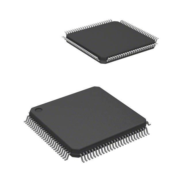


 工商网监
湘ICP备2023018690号
工商网监
湘ICP备2023018690号
