STM32F401xB STM32F401xC
Arm® Cortex®-M4 32-bit MCU+FPU, 105 DMIPS,
256KB Flash / 64KB RAM, 11 TIMs, 1 ADC, 11 comm. interfaces
Datasheet - production data
Features
• Dynamic efficiency line with BAM (batch
acquisition mode)
– 1.7 V to 3.6 V power supply
– -40 °C to 85/105/125 °C temperature range
• Core: Arm® 32-bit Cortex®-M4 CPU with FPU,
Adaptive real-time accelerator (ART
Accelerator™) allowing 0-wait state execution
from Flash memory, frequency up to 84 MHz,
memory protection unit, 105 DMIPS/
1.25 DMIPS/MHz (Dhrystone 2.1), and DSP
instructions
• Memories
– Up to 256 Kbytes of Flash memory
– 512 bytes of OTP memory
– Up to 64 Kbytes of SRAM
• Clock, reset and supply management
– 1.7 V to 3.6 V application supply and I/Os
– POR, PDR, PVD and BOR
– 4-to-26 MHz crystal oscillator
– Internal 16 MHz factory-trimmed RC
– 32 kHz oscillator for RTC with calibration
– Internal 32 kHz RC with calibration
• Power consumption
– Run: 128 µA/MHz (peripheral off)
– Stop (Flash in Stop mode, fast wakeup
time): 42 µA typ @ 25 °C;
65 µA max @25 °C
– Stop (Flash in Deep power down mode,
slow wakeup time): down to 10 µA typ@
25 °C; 28 µA max @25 °C
– Standby: 2.4 µA @25 °C / 1.7 V without
RTC; 12 µA @85 °C @1.7 V
– VBAT supply for RTC: 1 µA @25 °C
• 1×12-bit, 2.4 MSPS A/D converter: up to 16
channels
• General-purpose DMA: 16-stream DMA
controllers with FIFOs and burst support
• Up to 11 timers: up to six 16-bit, two 32-bit
timers up to 84 MHz, each with up to
4 IC/OC/PWM or pulse counter and quadrature
April 2019
This is information on a product in full production.
)%*$
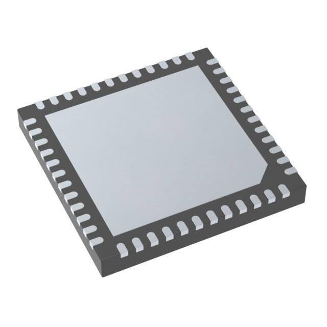
WLCSP49
UFQFPN48
UFBGA100 LQFP100 (14X14 mm)
(7×7 mm) (2.965x2.965 mm) (7x7 mm)
LQFP64 (10×10 mm)
(incremental) encoder input, two watchdog
timers (independent and window) and a
SysTick timer
• Debug mode
– Serial wire debug (SWD) & JTAG
interfaces
– Cortex®-M4 Embedded Trace Macrocell™
• Up to 81 I/O ports with interrupt capability
– All IO ports 5 V tolerant
– Up to 78 fast I/Os up to 42 MHz
• Up to 11 communication interfaces
– Up to 3 × I2C interfaces (1Mbit/s,
SMBus/PMBus)
– Up to 3 USARTs (2 x 10.5 Mbit/s, 1 x
5.25 Mbit/s), ISO 7816 interface, LIN, IrDA,
modem control)
– Up to 4 SPIs (up to 42 Mbits/s at fCPU = 84
MHz), SPI2 and SPI3 with muxed fullduplex I2S to achieve audio class accuracy
via internal audio PLL or external clock
– SDIO interface
• Advanced connectivity
– USB 2.0 full-speed device/host/OTG
controller with on-chip PHY
• CRC calculation unit
• 96-bit unique ID
• RTC: subsecond accuracy, hardware calendar
• All packages are ECOPACK2
Table 1. Device summary
Reference
Part number
STM32F401xB
STM32F401CB, STM32F401RB,
STM32F401VB
STM32F401xC
STM32F401CC, STM32F401RC,
STM32F401VC
DS9716 Rev 11
1/139
www.st.com
�Contents
STM32F401xB STM32F401xC
Contents
1
Introduction . . . . . . . . . . . . . . . . . . . . . . . . . . . . . . . . . . . . . . . . . . . . . . . . 9
2
Description . . . . . . . . . . . . . . . . . . . . . . . . . . . . . . . . . . . . . . . . . . . . . . . . 10
2.1
3
Functional overview . . . . . . . . . . . . . . . . . . . . . . . . . . . . . . . . . . . . . . . . 15
3.1
Arm® Cortex®-M4 with FPU core with embedded Flash and SRAM . . . . 15
3.2
Adaptive real-time memory accelerator (ART Accelerator™) . . . . . . . . . 15
3.3
Memory protection unit . . . . . . . . . . . . . . . . . . . . . . . . . . . . . . . . . . . . . . . 15
3.4
Embedded Flash memory . . . . . . . . . . . . . . . . . . . . . . . . . . . . . . . . . . . . 16
3.5
CRC (cyclic redundancy check) calculation unit . . . . . . . . . . . . . . . . . . . 16
3.6
Embedded SRAM . . . . . . . . . . . . . . . . . . . . . . . . . . . . . . . . . . . . . . . . . . . 16
3.7
Multi-AHB bus matrix . . . . . . . . . . . . . . . . . . . . . . . . . . . . . . . . . . . . . . . . 16
3.8
DMA controller (DMA) . . . . . . . . . . . . . . . . . . . . . . . . . . . . . . . . . . . . . . . 17
3.9
Nested vectored interrupt controller (NVIC) . . . . . . . . . . . . . . . . . . . . . . . 17
3.10
External interrupt/event controller (EXTI) . . . . . . . . . . . . . . . . . . . . . . . . . 17
3.11
Clocks and startup . . . . . . . . . . . . . . . . . . . . . . . . . . . . . . . . . . . . . . . . . . 18
3.12
Boot modes . . . . . . . . . . . . . . . . . . . . . . . . . . . . . . . . . . . . . . . . . . . . . . . 18
3.13
Power supply schemes . . . . . . . . . . . . . . . . . . . . . . . . . . . . . . . . . . . . . . 18
3.14
Power supply supervisor . . . . . . . . . . . . . . . . . . . . . . . . . . . . . . . . . . . . . 19
3.15
2/139
Compatibility with STM32F4 Series . . . . . . . . . . . . . . . . . . . . . . . . . . . . . 12
3.14.1
Internal reset ON . . . . . . . . . . . . . . . . . . . . . . . . . . . . . . . . . . . . . . . . . . 19
3.14.2
Internal reset OFF . . . . . . . . . . . . . . . . . . . . . . . . . . . . . . . . . . . . . . . . . 19
Voltage regulator . . . . . . . . . . . . . . . . . . . . . . . . . . . . . . . . . . . . . . . . . . . 20
3.15.1
Regulator ON . . . . . . . . . . . . . . . . . . . . . . . . . . . . . . . . . . . . . . . . . . . . . 21
3.15.2
Regulator OFF . . . . . . . . . . . . . . . . . . . . . . . . . . . . . . . . . . . . . . . . . . . . 21
3.15.3
Regulator ON/OFF and internal power supply supervisor availability . . 24
3.16
Real-time clock (RTC) and backup registers . . . . . . . . . . . . . . . . . . . . . . 24
3.17
Low-power modes . . . . . . . . . . . . . . . . . . . . . . . . . . . . . . . . . . . . . . . . . . 25
3.18
VBAT operation . . . . . . . . . . . . . . . . . . . . . . . . . . . . . . . . . . . . . . . . . . . . . 25
3.19
Timers and watchdogs . . . . . . . . . . . . . . . . . . . . . . . . . . . . . . . . . . . . . . . 25
3.19.1
Advanced-control timers (TIM1) . . . . . . . . . . . . . . . . . . . . . . . . . . . . . . 26
3.19.2
General-purpose timers (TIMx) . . . . . . . . . . . . . . . . . . . . . . . . . . . . . . . 27
DS9716 Rev 11
�STM32F401xB STM32F401xC
Contents
3.19.3
Independent watchdog . . . . . . . . . . . . . . . . . . . . . . . . . . . . . . . . . . . . . 27
3.19.4
Window watchdog . . . . . . . . . . . . . . . . . . . . . . . . . . . . . . . . . . . . . . . . . 27
3.19.5
SysTick timer . . . . . . . . . . . . . . . . . . . . . . . . . . . . . . . . . . . . . . . . . . . . . 27
3.20
Inter-integrated circuit interface (I2C) . . . . . . . . . . . . . . . . . . . . . . . . . . . . 28
3.21
Universal synchronous/asynchronous receiver transmitters (USART) . . 28
3.22
Serial peripheral interface (SPI) . . . . . . . . . . . . . . . . . . . . . . . . . . . . . . . . 29
3.23
Inter-integrated sound (I2S) . . . . . . . . . . . . . . . . . . . . . . . . . . . . . . . . . . . 29
3.24
Audio PLL (PLLI2S) . . . . . . . . . . . . . . . . . . . . . . . . . . . . . . . . . . . . . . . . . 29
3.25
Secure digital input/output interface (SDIO) . . . . . . . . . . . . . . . . . . . . . . . 29
3.26
Universal serial bus on-the-go full-speed (OTG_FS) . . . . . . . . . . . . . . . . 30
3.27
General-purpose input/outputs (GPIOs) . . . . . . . . . . . . . . . . . . . . . . . . . . 30
3.28
Analog-to-digital converter (ADC) . . . . . . . . . . . . . . . . . . . . . . . . . . . . . . 30
3.29
Temperature sensor . . . . . . . . . . . . . . . . . . . . . . . . . . . . . . . . . . . . . . . . . 30
3.30
Serial wire JTAG debug port (SWJ-DP) . . . . . . . . . . . . . . . . . . . . . . . . . . 31
3.31
Embedded Trace Macrocell™ . . . . . . . . . . . . . . . . . . . . . . . . . . . . . . . . . 31
4
Pinouts and pin description . . . . . . . . . . . . . . . . . . . . . . . . . . . . . . . . . . 32
5
Memory mapping . . . . . . . . . . . . . . . . . . . . . . . . . . . . . . . . . . . . . . . . . . . 50
6
Electrical characteristics . . . . . . . . . . . . . . . . . . . . . . . . . . . . . . . . . . . . 54
6.1
Parameter conditions . . . . . . . . . . . . . . . . . . . . . . . . . . . . . . . . . . . . . . . . 54
6.1.1
Minimum and maximum values . . . . . . . . . . . . . . . . . . . . . . . . . . . . . . . 54
6.1.2
Typical values . . . . . . . . . . . . . . . . . . . . . . . . . . . . . . . . . . . . . . . . . . . . 54
6.1.3
Typical curves . . . . . . . . . . . . . . . . . . . . . . . . . . . . . . . . . . . . . . . . . . . . 54
6.1.4
Loading capacitor . . . . . . . . . . . . . . . . . . . . . . . . . . . . . . . . . . . . . . . . . 54
6.1.5
Pin input voltage . . . . . . . . . . . . . . . . . . . . . . . . . . . . . . . . . . . . . . . . . . 55
6.1.6
Power supply scheme . . . . . . . . . . . . . . . . . . . . . . . . . . . . . . . . . . . . . . 56
6.1.7
Current consumption measurement . . . . . . . . . . . . . . . . . . . . . . . . . . . 57
6.2
Absolute maximum ratings . . . . . . . . . . . . . . . . . . . . . . . . . . . . . . . . . . . . 57
6.3
Operating conditions . . . . . . . . . . . . . . . . . . . . . . . . . . . . . . . . . . . . . . . . 59
6.3.1
General operating conditions . . . . . . . . . . . . . . . . . . . . . . . . . . . . . . . . . 59
6.3.2
VCAP_1/VCAP_2 external capacitors . . . . . . . . . . . . . . . . . . . . . . . . . . 61
6.3.3
Operating conditions at power-up / power-down (regulator ON) . . . . . . 61
6.3.4
Operating conditions at power-up / power-down (regulator OFF) . . . . . 62
6.3.5
Embedded reset and power control block characteristics . . . . . . . . . . . 62
DS9716 Rev 11
3/139
4
�Contents
7
STM32F401xB STM32F401xC
6.3.6
Supply current characteristics . . . . . . . . . . . . . . . . . . . . . . . . . . . . . . . . 63
6.3.7
Wakeup time from low-power modes . . . . . . . . . . . . . . . . . . . . . . . . . . . 74
6.3.8
External clock source characteristics . . . . . . . . . . . . . . . . . . . . . . . . . . . 75
6.3.9
Internal clock source characteristics . . . . . . . . . . . . . . . . . . . . . . . . . . . 79
6.3.10
PLL characteristics . . . . . . . . . . . . . . . . . . . . . . . . . . . . . . . . . . . . . . . . 81
6.3.11
PLL spread spectrum clock generation (SSCG) characteristics . . . . . . 83
6.3.12
Memory characteristics . . . . . . . . . . . . . . . . . . . . . . . . . . . . . . . . . . . . . 84
6.3.13
EMC characteristics . . . . . . . . . . . . . . . . . . . . . . . . . . . . . . . . . . . . . . . . 86
6.3.14
Absolute maximum ratings (electrical sensitivity) . . . . . . . . . . . . . . . . . 88
6.3.15
I/O current injection characteristics . . . . . . . . . . . . . . . . . . . . . . . . . . . . 89
6.3.16
I/O port characteristics . . . . . . . . . . . . . . . . . . . . . . . . . . . . . . . . . . . . . . 90
6.3.17
NRST pin characteristics . . . . . . . . . . . . . . . . . . . . . . . . . . . . . . . . . . . . 94
6.3.18
TIM timer characteristics . . . . . . . . . . . . . . . . . . . . . . . . . . . . . . . . . . . . 95
6.3.19
Communications interfaces . . . . . . . . . . . . . . . . . . . . . . . . . . . . . . . . . . 96
6.3.20
12-bit ADC characteristics . . . . . . . . . . . . . . . . . . . . . . . . . . . . . . . . . . 104
6.3.21
Temperature sensor characteristics . . . . . . . . . . . . . . . . . . . . . . . . . . . 110
6.3.22
VBAT monitoring characteristics . . . . . . . . . . . . . . . . . . . . . . . . . . . . . . 111
6.3.23
Embedded reference voltage . . . . . . . . . . . . . . . . . . . . . . . . . . . . . . . . 111
6.3.24
SD/SDIO MMC card host interface (SDIO) characteristics . . . . . . . . . 111
6.3.25
RTC characteristics . . . . . . . . . . . . . . . . . . . . . . . . . . . . . . . . . . . . . . . 113
Package information . . . . . . . . . . . . . . . . . . . . . . . . . . . . . . . . . . . . . . . 114
7.1
WLCSP49 package information . . . . . . . . . . . . . . . . . . . . . . . . . . . . . . . .114
7.2
UFQFPN48 package information . . . . . . . . . . . . . . . . . . . . . . . . . . . . . . .117
7.3
LQFP64 package information . . . . . . . . . . . . . . . . . . . . . . . . . . . . . . . . . 120
7.4
LQFP100 package information . . . . . . . . . . . . . . . . . . . . . . . . . . . . . . . . 124
7.5
UFBGA100 package information . . . . . . . . . . . . . . . . . . . . . . . . . . . . . . 128
7.6
Thermal characteristics . . . . . . . . . . . . . . . . . . . . . . . . . . . . . . . . . . . . . 131
7.6.1
Reference document . . . . . . . . . . . . . . . . . . . . . . . . . . . . . . . . . . . . . . 131
8
Ordering information . . . . . . . . . . . . . . . . . . . . . . . . . . . . . . . . . . . . . . 132
9
Revision history . . . . . . . . . . . . . . . . . . . . . . . . . . . . . . . . . . . . . . . . . . 133
4/139
DS9716 Rev 11
�STM32F401xB STM32F401xC
List of tables
List of tables
Table 1.
Table 2.
Table 3.
Table 4.
Table 5.
Table 6.
Table 7.
Table 8.
Table 9.
Table 10.
Table 11.
Table 12.
Table 13.
Table 14.
Table 15.
Table 16.
Table 17.
Table 18.
Table 19.
Table 20.
Table 21.
Table 22.
Table 23.
Table 24.
Table 25.
Table 26.
Table 27.
Table 28.
Table 29.
Table 30.
Table 31.
Table 32.
Table 33.
Table 34.
Table 35.
Table 36.
Table 37.
Table 38.
Table 39.
Table 40.
Table 41.
Device summary . . . . . . . . . . . . . . . . . . . . . . . . . . . . . . . . . . . . . . . . . . . . . . . . . . . . . . . . . . 1
STM32F401xB/C features and peripheral counts. . . . . . . . . . . . . . . . . . . . . . . . . . . . . . . . 11
Regulator ON/OFF and internal power supply supervisor availability. . . . . . . . . . . . . . . . . 24
Timer feature comparison . . . . . . . . . . . . . . . . . . . . . . . . . . . . . . . . . . . . . . . . . . . . . . . . . . 26
Comparison of I2C analog and digital filters . . . . . . . . . . . . . . . . . . . . . . . . . . . . . . . . . . . . 28
USART feature comparison . . . . . . . . . . . . . . . . . . . . . . . . . . . . . . . . . . . . . . . . . . . . . . . . 28
Legend/abbreviations used in the pinout table . . . . . . . . . . . . . . . . . . . . . . . . . . . . . . . . . . 37
STM32F401xB/STM32F401xC pin definitions . . . . . . . . . . . . . . . . . . . . . . . . . . . . . . . . . . 37
Alternate function mapping . . . . . . . . . . . . . . . . . . . . . . . . . . . . . . . . . . . . . . . . . . . . . . . . . 44
STM32F401xB/STM32F401xC
register boundary addresses . . . . . . . . . . . . . . . . . . . . . . . . . . . . . . . . . . . . . . . . . . . . . . . 51
Voltage characteristics . . . . . . . . . . . . . . . . . . . . . . . . . . . . . . . . . . . . . . . . . . . . . . . . . . . . 57
Current characteristics . . . . . . . . . . . . . . . . . . . . . . . . . . . . . . . . . . . . . . . . . . . . . . . . . . . . 58
Thermal characteristics. . . . . . . . . . . . . . . . . . . . . . . . . . . . . . . . . . . . . . . . . . . . . . . . . . . . 58
General operating conditions . . . . . . . . . . . . . . . . . . . . . . . . . . . . . . . . . . . . . . . . . . . . . . . 59
Features depending on the operating power supply range . . . . . . . . . . . . . . . . . . . . . . . . 60
VCAP_1/VCAP_2 operating conditions . . . . . . . . . . . . . . . . . . . . . . . . . . . . . . . . . . . . . . . 61
Operating conditions at power-up / power-down (regulator ON) . . . . . . . . . . . . . . . . . . . . 61
Operating conditions at power-up / power-down (regulator OFF). . . . . . . . . . . . . . . . . . . . 62
Embedded reset and power control block characteristics. . . . . . . . . . . . . . . . . . . . . . . . . . 62
Typical and maximum current consumption, code with data processing (ART
accelerator disabled) running from SRAM - VDD = 1.8 V . . . . . . . . . . . . . . . . . . . . . . . . . . 64
Typical and maximum current consumption, code with data processing (ART
accelerator disabled) running from SRAM . . . . . . . . . . . . . . . . . . . . . . . . . . . . . . . . . . . . . 65
Typical and maximum current consumption in run mode, code with data processing
(ART accelerator enabled except prefetch) running from Flash memory- VDD = 1.8 V . . . 65
Typical and maximum current consumption in run mode, code with data processing
(ART accelerator enabled except prefetch) running from Flash memory - VDD = 3.3 V . . 66
Typical and maximum current consumption in run mode, code with data processing
(ART accelerator disabled) running from Flash memory . . . . . . . . . . . . . . . . . . . . . . . . . . 66
Typical and maximum current consumption in run mode, code with data processing
(ART accelerator enabled with prefetch) running from Flash memory . . . . . . . . . . . . . . . . 67
Typical and maximum current consumption in Sleep mode . . . . . . . . . . . . . . . . . . . . . . . . 67
Typical and maximum current consumptions in Stop mode - VDD = 1.8 V . . . . . . . . . . . . . 68
Typical and maximum current consumption in Stop mode - VDD=3.3 V. . . . . . . . . . . . . . . 68
Typical and maximum current consumption in Standby mode - VDD= 1.8 V . . . . . . . . . . . 68
Typical and maximum current consumption in Standby mode - VDD=3.3 V . . . . . . . . . . . . 69
Typical and maximum current consumptions in VBAT mode. . . . . . . . . . . . . . . . . . . . . . . . 69
Switching output I/O current consumption . . . . . . . . . . . . . . . . . . . . . . . . . . . . . . . . . . . . . 72
Peripheral current consumption . . . . . . . . . . . . . . . . . . . . . . . . . . . . . . . . . . . . . . . . . . . . . 73
Low-power mode wakeup timings(1) . . . . . . . . . . . . . . . . . . . . . . . . . . . . . . . . . . . . . . . . . . 74
High-speed external user clock characteristics. . . . . . . . . . . . . . . . . . . . . . . . . . . . . . . . . . 75
Low-speed external user clock characteristics . . . . . . . . . . . . . . . . . . . . . . . . . . . . . . . . . . 76
HSE 4-26 MHz oscillator characteristics. . . . . . . . . . . . . . . . . . . . . . . . . . . . . . . . . . . . . . . 77
LSE oscillator characteristics (fLSE = 32.768 kHz) . . . . . . . . . . . . . . . . . . . . . . . . . . . . . . . 78
HSI oscillator characteristics . . . . . . . . . . . . . . . . . . . . . . . . . . . . . . . . . . . . . . . . . . . . . . . 79
LSI oscillator characteristics . . . . . . . . . . . . . . . . . . . . . . . . . . . . . . . . . . . . . . . . . . . . . . . 80
Main PLL characteristics. . . . . . . . . . . . . . . . . . . . . . . . . . . . . . . . . . . . . . . . . . . . . . . . . . . 81
DS9716 Rev 11
5/139
6
�List of tables
Table 42.
Table 43.
Table 44.
Table 45.
Table 46.
Table 47.
Table 48.
Table 49.
Table 50.
Table 51.
Table 52.
Table 53.
Table 54.
Table 55.
Table 56.
Table 57.
Table 58.
Table 59.
Table 60.
Table 61.
Table 62.
Table 63.
Table 64.
Table 65.
Table 66.
Table 67.
Table 68.
Table 69.
Table 70.
Table 71.
Table 72.
Table 73.
Table 74.
Table 75.
Table 76.
Table 77.
Table 78.
Table 79.
Table 80.
Table 81.
Table 82.
Table 83.
Table 84.
Table 85.
Table 86.
Table 87.
6/139
STM32F401xB STM32F401xC
PLLI2S (audio PLL) characteristics . . . . . . . . . . . . . . . . . . . . . . . . . . . . . . . . . . . . . . . . . . 82
SSCG parameters constraint . . . . . . . . . . . . . . . . . . . . . . . . . . . . . . . . . . . . . . . . . . . . . . . 83
Flash memory characteristics . . . . . . . . . . . . . . . . . . . . . . . . . . . . . . . . . . . . . . . . . . . . . . . 84
Flash memory programming . . . . . . . . . . . . . . . . . . . . . . . . . . . . . . . . . . . . . . . . . . . . . . . . 85
Flash memory programming with VPP voltage . . . . . . . . . . . . . . . . . . . . . . . . . . . . . . . . . . 85
Flash memory endurance and data retention . . . . . . . . . . . . . . . . . . . . . . . . . . . . . . . . . . . 86
EMS characteristics for LQFP100 package . . . . . . . . . . . . . . . . . . . . . . . . . . . . . . . . . . . . 87
EMI characteristics for WLCSP49 . . . . . . . . . . . . . . . . . . . . . . . . . . . . . . . . . . . . . . . . . . . 88
EMI characteristics for LQFP100 . . . . . . . . . . . . . . . . . . . . . . . . . . . . . . . . . . . . . . . . . . . . 88
ESD absolute maximum ratings . . . . . . . . . . . . . . . . . . . . . . . . . . . . . . . . . . . . . . . . . . . . . 88
Electrical sensitivities . . . . . . . . . . . . . . . . . . . . . . . . . . . . . . . . . . . . . . . . . . . . . . . . . . . . . 89
I/O current injection susceptibility . . . . . . . . . . . . . . . . . . . . . . . . . . . . . . . . . . . . . . . . . . . . 89
I/O static characteristics . . . . . . . . . . . . . . . . . . . . . . . . . . . . . . . . . . . . . . . . . . . . . . . . . . . 90
Output voltage characteristics . . . . . . . . . . . . . . . . . . . . . . . . . . . . . . . . . . . . . . . . . . . . . . 92
I/O AC characteristics . . . . . . . . . . . . . . . . . . . . . . . . . . . . . . . . . . . . . . . . . . . . . . . . . . . . . 93
NRST pin characteristics . . . . . . . . . . . . . . . . . . . . . . . . . . . . . . . . . . . . . . . . . . . . . . . . . . 94
TIMx characteristics . . . . . . . . . . . . . . . . . . . . . . . . . . . . . . . . . . . . . . . . . . . . . . . . . . . . . . 95
I2C characteristics. . . . . . . . . . . . . . . . . . . . . . . . . . . . . . . . . . . . . . . . . . . . . . . . . . . . . . . . 96
SCL frequency (fPCLK1= 42 MHz, VDD = VDD_I2C = 3.3 V) . . . . . . . . . . . . . . . . . . . . . . . . . 97
SPI dynamic characteristics . . . . . . . . . . . . . . . . . . . . . . . . . . . . . . . . . . . . . . . . . . . . . . . . 98
I2S dynamic characteristics . . . . . . . . . . . . . . . . . . . . . . . . . . . . . . . . . . . . . . . . . . . . . . . 101
USB OTG FS startup time . . . . . . . . . . . . . . . . . . . . . . . . . . . . . . . . . . . . . . . . . . . . . . . . 103
USB OTG FS DC electrical characteristics. . . . . . . . . . . . . . . . . . . . . . . . . . . . . . . . . . . . 103
USB OTG FS electrical characteristics . . . . . . . . . . . . . . . . . . . . . . . . . . . . . . . . . . . . . . . 104
ADC characteristics . . . . . . . . . . . . . . . . . . . . . . . . . . . . . . . . . . . . . . . . . . . . . . . . . . . . . 104
ADC accuracy at fADC = 18 MHz . . . . . . . . . . . . . . . . . . . . . . . . . . . . . . . . . . . . . . . . . . . 106
ADC accuracy at fADC = 30 MHz . . . . . . . . . . . . . . . . . . . . . . . . . . . . . . . . . . . . . . . . . . . 106
ADC accuracy at fADC = 36 MHz . . . . . . . . . . . . . . . . . . . . . . . . . . . . . . . . . . . . . . . . . . . 106
ADC dynamic accuracy at fADC = 18 MHz - limited test conditions . . . . . . . . . . . . . . . . . 107
ADC dynamic accuracy at fADC = 36 MHz - limited test conditions . . . . . . . . . . . . . . . . . 107
Temperature sensor characteristics . . . . . . . . . . . . . . . . . . . . . . . . . . . . . . . . . . . . . . . . . 110
Temperature sensor calibration values. . . . . . . . . . . . . . . . . . . . . . . . . . . . . . . . . . . . . . . 110
VBAT monitoring characteristics . . . . . . . . . . . . . . . . . . . . . . . . . . . . . . . . . . . . . . . . . . . . 111
Embedded internal reference voltage . . . . . . . . . . . . . . . . . . . . . . . . . . . . . . . . . . . . . . . . 111
Internal reference voltage calibration values . . . . . . . . . . . . . . . . . . . . . . . . . . . . . . . . . . 111
Dynamic characteristics: SD / MMC characteristics . . . . . . . . . . . . . . . . . . . . . . . . . . . . . 112
RTC characteristics . . . . . . . . . . . . . . . . . . . . . . . . . . . . . . . . . . . . . . . . . . . . . . . . . . . . . 113
WLCSP49 - 49-ball, 2.965 x 2.965 mm, 0.4 mm pitch wafer level chip scale
package mechanical data . . . . . . . . . . . . . . . . . . . . . . . . . . . . . . . . . . . . . . . . . . . . . . . . 115
WLCSP49 recommended PCB design rules (0.4 mm pitch) . . . . . . . . . . . . . . . . . . . . . . 116
UFQFPN48 - 48-lead, 7 x 7 mm, 0.5 mm pitch, ultra thin fine pitch
quad flat package mechanical data . . . . . . . . . . . . . . . . . . . . . . . . . . . . . . . . . . . . . . . . . 117
LQFP64 - 64-pin, 10 x 10 mm low-profile quad flat
package mechanical data . . . . . . . . . . . . . . . . . . . . . . . . . . . . . . . . . . . . . . . . . . . . . . . . . 120
LQPF100 - 100-pin, 14 x 14 mm, 100-pin low-profile quad flat package mechanical data125
UFBGA100 - 100-ball, 7 x 7 mm, 0.50 mm pitch, ultra fine pitch ball grid array
package mechanical data . . . . . . . . . . . . . . . . . . . . . . . . . . . . . . . . . . . . . . . . . . . . . . . . . 128
UFBGA100 recommended PCB design rules (0.5 mm pitch BGA) . . . . . . . . . . . . . . . . . 129
Package thermal characteristics . . . . . . . . . . . . . . . . . . . . . . . . . . . . . . . . . . . . . . . . . . . . 131
Document revision history . . . . . . . . . . . . . . . . . . . . . . . . . . . . . . . . . . . . . . . . . . . . . . . . 133
DS9716 Rev 11
�STM32F401xB STM32F401xC
List of figures
List of figures
Figure 1.
Figure 2.
Figure 3.
Figure 4.
Figure 5.
Figure 6.
Figure 7.
Figure 8.
Figure 9.
Figure 10.
Figure 11.
Figure 12.
Figure 13.
Figure 14.
Figure 15.
Figure 16.
Figure 17.
Figure 18.
Figure 19.
Figure 20.
Figure 21.
Figure 22.
Figure 23.
Figure 24.
Figure 25.
Figure 26.
Figure 27.
Figure 28.
Figure 29.
Figure 30.
Figure 31.
Figure 32.
Figure 33.
Figure 34.
Figure 35.
Figure 36.
Figure 37.
Figure 38.
Figure 39.
Figure 40.
Figure 41.
Figure 42.
Figure 43.
Figure 44.
Figure 45.
Figure 46.
Compatible board design for LQFP100 package . . . . . . . . . . . . . . . . . . . . . . . . . . . . . . . . 12
Compatible board design for LQFP64 package . . . . . . . . . . . . . . . . . . . . . . . . . . . . . . . . . 13
STM32F401xB/STM32F401xC block diagram
. . . . . . . . . . . . . . . . . . . . . . . . . . . . . . 14
Multi-AHB matrix . . . . . . . . . . . . . . . . . . . . . . . . . . . . . . . . . . . . . . . . . . . . . . . . . . . . . . . 16
Power supply supervisor interconnection with internal reset OFF . . . . . . . . . . . . . . . . . . . 19
PDR_ON control with internal reset OFF . . . . . . . . . . . . . . . . . . . . . . . . . . . . . . . . . . . . . . 20
Regulator OFF . . . . . . . . . . . . . . . . . . . . . . . . . . . . . . . . . . . . . . . . . . . . . . . . . . . . . . . . . . 22
Startup in regulator OFF: slow VDD slope power-down reset risen after VCAP_1/VCAP_2 stabilization. . . . . . . . . . . . . . . . . . . . . . . . . 23
Startup in regulator OFF mode: fast VDD slope power-down reset risen before VCAP_1/VCAP_2 stabilization . . . . . . . . . . . . . . . . . . . . . . . 23
STM32F401xB/STM32F401xC WLCSP49 pinout . . . . . . . . . . . . . . . . . . . . . . . . . . . . . . . 32
STM32F401xB/STM32F401xC UFQFPN48 pinout . . . . . . . . . . . . . . . . . . . . . . . . . . . . . . 33
STM32F401xB/STM32F401xC LQFP64 pinout . . . . . . . . . . . . . . . . . . . . . . . . . . . . . . . . . 34
STM32F401xB/STM32F401xC LQFP100 pinout . . . . . . . . . . . . . . . . . . . . . . . . . . . . . . . . 35
STM32F401xB/STM32F401xC UFBGA100 pinout . . . . . . . . . . . . . . . . . . . . . . . . . . . . . . 36
Memory map . . . . . . . . . . . . . . . . . . . . . . . . . . . . . . . . . . . . . . . . . . . . . . . . . . . . . . . . . . 50
Pin loading conditions . . . . . . . . . . . . . . . . . . . . . . . . . . . . . . . . . . . . . . . . . . . . . . . . . . . . . 54
Input voltage measurement . . . . . . . . . . . . . . . . . . . . . . . . . . . . . . . . . . . . . . . . . . . . . . . . 55
Power supply scheme . . . . . . . . . . . . . . . . . . . . . . . . . . . . . . . . . . . . . . . . . . . . . . . . . . . . 56
Current consumption measurement scheme . . . . . . . . . . . . . . . . . . . . . . . . . . . . . . . . . . . 57
External capacitor CEXT . . . . . . . . . . . . . . . . . . . . . . . . . . . . . . . . . . . . . . . . . . . . . . . . . . . 61
Typical VBAT current consumption (LSE and RTC ON) . . . . . . . . . . . . . . . . . . . . . . . . . . . 70
High-speed external clock source AC timing diagram . . . . . . . . . . . . . . . . . . . . . . . . . . . . 76
Low-speed external clock source AC timing diagram . . . . . . . . . . . . . . . . . . . . . . . . . . . . . 77
Typical application with an 8 MHz crystal . . . . . . . . . . . . . . . . . . . . . . . . . . . . . . . . . . . . . . 78
Typical application with a 32.768 kHz crystal . . . . . . . . . . . . . . . . . . . . . . . . . . . . . . . . . . . 79
ACCHSI versus temperature . . . . . . . . . . . . . . . . . . . . . . . . . . . . . . . . . . . . . . . . . . . . . . . . 80
ACCLSI versus temperature . . . . . . . . . . . . . . . . . . . . . . . . . . . . . . . . . . . . . . . . . . . . . . . . 81
PLL output clock waveforms in center spread mode . . . . . . . . . . . . . . . . . . . . . . . . . . . . . 84
PLL output clock waveforms in down spread mode . . . . . . . . . . . . . . . . . . . . . . . . . . . . . . 84
FT I/O input characteristics . . . . . . . . . . . . . . . . . . . . . . . . . . . . . . . . . . . . . . . . . . . . . . . . . 91
I/O AC characteristics definition . . . . . . . . . . . . . . . . . . . . . . . . . . . . . . . . . . . . . . . . . . . . . 94
Recommended NRST pin protection . . . . . . . . . . . . . . . . . . . . . . . . . . . . . . . . . . . . . . . . . 95
I2C bus AC waveforms and measurement circuit . . . . . . . . . . . . . . . . . . . . . . . . . . . . . . . . 97
SPI timing diagram - slave mode and CPHA = 0 . . . . . . . . . . . . . . . . . . . . . . . . . . . . . . . . 99
SPI timing diagram - slave mode and CPHA = 1(1) . . . . . . . . . . . . . . . . . . . . . . . . . . . . . . 99
SPI timing diagram - master mode(1) . . . . . . . . . . . . . . . . . . . . . . . . . . . . . . . . . . . . . . . . 100
I2S slave timing diagram (Philips protocol)(1) . . . . . . . . . . . . . . . . . . . . . . . . . . . . . . . . . . 102
I2S master timing diagram (Philips protocol)(1) . . . . . . . . . . . . . . . . . . . . . . . . . . . . . . . . . 102
USB OTG FS timings: definition of data signal rise and fall time . . . . . . . . . . . . . . . . . . . 104
ADC accuracy characteristics . . . . . . . . . . . . . . . . . . . . . . . . . . . . . . . . . . . . . . . . . . . . . . 108
Typical connection diagram using the ADC . . . . . . . . . . . . . . . . . . . . . . . . . . . . . . . . . . . 108
Power supply and reference decoupling (VREF+ not connected to VDDA). . . . . . . . . . . . . 109
Power supply and reference decoupling (VREF+ connected to VDDA). . . . . . . . . . . . . . . . 110
SDIO high-speed mode . . . . . . . . . . . . . . . . . . . . . . . . . . . . . . . . . . . . . . . . . . . . . . . . . . 112
SD default mode . . . . . . . . . . . . . . . . . . . . . . . . . . . . . . . . . . . . . . . . . . . . . . . . . . . . . . . . 112
WLCSP49 - 49-ball, 2.965 x 2.965 mm, 0.4 mm pitch wafer level chip scale
DS9716 Rev 11
7/139
8
�List of figures
Figure 47.
Figure 48.
Figure 49.
Figure 50.
Figure 51.
Figure 52.
Figure 53.
Figure 54.
Figure 55.
Figure 56.
Figure 57.
Figure 58.
Figure 59.
Figure 60.
Figure 61.
8/139
STM32F401xB STM32F401xC
package outline . . . . . . . . . . . . . . . . . . . . . . . . . . . . . . . . . . . . . . . . . . . . . . . . . . . . . . . . 114
WLCSP49 - 49-ball, 2.999 mm, 0.4 mm pitch wafer level chip scale
recommended footprint . . . . . . . . . . . . . . . . . . . . . . . . . . . . . . . . . . . . . . . . . . . . . . . . . . . 115
WLCSP49 marking example (package top view) . . . . . . . . . . . . . . . . . . . . . . . . . . . . . . . 116
UFQFPN48 - 48-lead, 7 x 7 mm, 0.5 mm pitch, ultra thin fine pitch
quad flat package outline . . . . . . . . . . . . . . . . . . . . . . . . . . . . . . . . . . . . . . . . . . . . . . . . . 117
UFQFPN48 - 48-lead, 7 x 7 mm, 0.5 mm pitch, ultra thin fine pitch
quad flat recommended footprint . . . . . . . . . . . . . . . . . . . . . . . . . . . . . . . . . . . . . . . . . . . 118
UFQFPN48 marking example (package top view) . . . . . . . . . . . . . . . . . . . . . . . . . . . . . . 119
LQFP64 - 64-pin, 10 x 10 mm low-profile quad flat package outline . . . . . . . . . . . . . . . . 120
LQFP64 - 64-pin, 10 x 10 mm low-profile quad flat package
recommended footprint . . . . . . . . . . . . . . . . . . . . . . . . . . . . . . . . . . . . . . . . . . . . . . . . . . . 121
LQFP64 marking example (package top view) . . . . . . . . . . . . . . . . . . . . . . . . . . . . . . . . 122
LQFP64 marking example (package top view) . . . . . . . . . . . . . . . . . . . . . . . . . . . . . . . . . 123
LQFP100 - 100-pin, 14 x 14 mm, 100-pin low-profile quad flat
package outline. . . . . . . . . . . . . . . . . . . . . . . . . . . . . . . . . . . . . . . . . . . . . . . . . . . . . . . . . 124
LQFP100 - 100-pin, 14 x 14 mm, 100-pin low-profile quad flat
recommended footprint . . . . . . . . . . . . . . . . . . . . . . . . . . . . . . . . . . . . . . . . . . . . . . . . . . . 126
LQPF100 marking example (package top view) . . . . . . . . . . . . . . . . . . . . . . . . . . . . . . . 127
UFBGA100 - 100-ball, 7 x 7 mm, 0.50 mm pitch, ultra fine pitch ball
grid array package outline . . . . . . . . . . . . . . . . . . . . . . . . . . . . . . . . . . . . . . . . . . . . . . . . 128
UFBGA100 - 100-ball, 7 x 7 mm, 0.50 mm pitch, ultra fine pitch ball grid array
package recommended footprint . . . . . . . . . . . . . . . . . . . . . . . . . . . . . . . . . . . . . . . . . . . 129
UFBGA100 marking example (package top view) . . . . . . . . . . . . . . . . . . . . . . . . . . . . . . 130
DS9716 Rev 11
�STM32F401xB STM32F401xC
1
Introduction
Introduction
This datasheet provides the description of the STM32F401xB/STM32F401xC
microcontrollers, based on an Arm® (a) core®.
This document has to be read in conjunction with RM0368 reference manual, which is
available from the STMicroelectronics website www.st.com. It includes all information
concerning Flash memory programming.
For information on the Cortex®-M4 core, refer to the Cortex®-M4 programming manual
(PM0214) available from www.st.com.
a. Arm is a registered trademark of Arm Limited (or its subsidiaries) in the US and/or elsewhere.
DS9716 Rev 11
9/139
53
�Description
2
STM32F401xB STM32F401xC
Description
The STM32F401XB/STM32F401XC devices are based on the high-performance
Arm® Cortex® -M4 32-bit RISC core operating at a frequency of up to 84 MHz.
The Cortex®-M4 core features a Floating point unit (FPU) single precision which supports all
Arm single-precision data-processing instructions and data types. It also implements a full
set of DSP instructions and a memory protection unit (MPU) which enhances application
security.
The STM32F401xB/STM32F401xC incorporate high-speed embedded memories (up to
256 Kbytes of Flash memory, up to 64 Kbytes of SRAM), and an extensive range of
enhanced I/Os and peripherals connected to two APB buses, two AHB buses and a 32-bit
multi-AHB bus matrix.
All devices offer one 12-bit ADC, a low-power RTC, six general-purpose 16-bit timers
including one PWM timer for motor control, two general-purpose 32-bit timers. They also
feature standard and advanced communication interfaces.
•
Up to three I2Cs
•
Up to four SPIs
•
Two full duplex I2Ss. To achieve audio class accuracy, the I2S peripherals can be
clocked via a dedicated internal audio PLL or via an external clock to allow
synchronization.
•
Three USARTs
•
SDIO interface
•
USB 2.0 OTG full speed interface
The STM32F401xB/STM32F401xC operate in the - 40 to + 125 °C temperature range from
a 1.7 (PDR OFF) to 3.6 V power supply. A comprehensive set of power-saving mode allows
the design of low-power applications.
These features make the STM32F401xB/STM32F401xC microcontrollers suitable for a
wide range of applications:
10/139
•
Motor drive and application control
•
Medical equipment
•
Industrial applications: PLC, inverters, circuit breakers
•
Printers, and scanners
•
Alarm systems, video intercom, and HVAC
•
Home audio appliances
•
Mobile phone sensor hub
DS9716 Rev 11
�STM32F401xB STM32F401xC
Description
Table 2. STM32F401xB/C features and peripheral counts
Peripherals
Flash memory in Kbytes
SRAM in
Kbytes
Timers
STM32F401xB
STM32F401xC
128
256
System
64
Generalpurpose
7
Advancedcontrol
1
SPI/ I2S
4/2 (full
duplex)
3/2 (full duplex)
Communication I2C
interfaces
USART
SDIO
3
3
-
1
-
USB OTG FS
GPIOs
12-bit ADC
Number of channels
36
50
81
36
50
81
1
10
16
10
16
84 MHz
Operating voltage
Package
1
1
Maximum CPU frequency
Operating temperatures
4/2 (full
duplex)
3/2 (full duplex)
1.7 to 3.6 V
Ambient temperatures: –40 to +85 °C/–40 to +105 °C/–40 to +125 °C
Junction temperature: –40 to + 130 °C
WLCSP49
UFQFPN48
LQFP64
UFBGA100
LQFP100
DS9716 Rev 11
WLCSP49
UFQFPN48
LQFP64
UFBGA100
LQFP100
11/139
53
�Description
2.1
STM32F401xB STM32F401xC
Compatibility with STM32F4 Series
The STM32F401xB/STM32F401xC are fully software and feature compatible with the
STM32F4 series (STM32F42x, STM32F43x, STM32F41x, STM32F405 and STM32F407)
The STM32F401xB/STM32F401xC can be used as drop-in replacement of the other
STM32F4 products but some slight changes have to be done on the PCB board.
Figure 1. Compatible board design for LQFP100 package
670��)����670��)����OLQH
670��)����670��)����OLQH
670��)����670��)����OLQH
670��)����670��)����OLQH
��
��
��
��
��
��
��
��
��
��
3(��
3(��
3(��
3(��
3(��
3(��
3%��
9&$3B�
966
9''
3%�� QRW DYDLODEOH�DQ\PRUH
5HSODFHG E\ 9 &$3B�
��
��
��
��
��
��
��
��
��
��
��
��
��
��
��
��
��
��
3'������
3'������
3'�
3'�
3%��
3%��
3%��
3%��
3(��
3(��
3(��
3(��
3(��
3(��
3%��
3%��
9&$3B�
9''
��
��
��
��
��
��
��
��
670��)���[[
670��)���[[
670��)���[[
670��)���[[
670��)���[[
670��)���[[
670��)���[[
966 9''
3'������
3'������
3'�
3'�
3%��
3%��
3%��
3%��
966 9''
06Y�����9�
12/139
DS9716 Rev 11
�STM32F401xB STM32F401xC
Description
Figure 2. Compatible board design for LQFP64 package
^dDϯϮ&ϰdžϭ
ϱϯ ϱϮ ϱϭ ϱϬ ϰϵ
ϰϴ
ϰϳ
s��
s��WϮ
W�ϭϯ
W�ϭϮ
W�ϭϭ
W�ϭϬ
W�ϵ
W�ϴ
W�ϵ
W�ϴ
W�ϳ
W�ϲ
W�ϭϱ
W�ϭϰ
W�ϭϯ
W�ϭϮ
s��
s^^
ϱϯ ϱϮ ϱϭ ϱϬ ϰϵ
ϰϴ
ϰϳ
ϰϲ
ϰϱ
ϰϰ
ϰϯ
ϰϮ
ϰϭ
ϰϬ
ϯϵ
ϯϴ
ϯϳ
W�ϭϭ�ŶŽƚ�ĂǀĂŝůĂďůĞ�ĂŶLJŵŽƌĞ��
ϯϲ
ZĞƉůĂĐĞĚ�ďLJ�s ��Wϭ
ϯϱ
ϯϰ
ϯϯ
Ϯϴ Ϯϵ ϯϬ ϯϭ ϯϮ
s��
s^^
W�ϭϯ
W�ϭϮ
W�ϭϭ
W�ϭϬ
W�ϵ
W�ϴ
W�ϵ
W�ϴ
W�ϳ
W�ϲ
W�ϭϱ
W�ϭϰ
W�ϭϯ
W�ϭϮ
s��
s^^
W�Ϯ
W�ϭϬ
s��Wϭ
s^^
s��
W�ϭϭ
s��Wϭ
s��
W�Ϯ
W�ϭϬ
ϰϲ
ϰϱ
ϰϰ
ϰϯ
ϰϮ
ϰϭ
ϰϬ
ϯϵ
ϯϴ
ϯϳ
ϯϲ
ϯϱ
ϯϰ
ϯϯ
Ϯϴ Ϯϵ ϯϬ ϯϭ ϯϮ
W�ϭϮ
W�ϭϭ
W�ϭϬ
W�ϭϱ
W�ϭϰ
W�ϭϮ
W�ϭϭ
W�ϭϬ
W�ϭϱ
W�ϭϰ
^dDϯϮ&ϰϬϱͬ^dDϯϮ&ϰϭϱ�ůŝŶĞ
s�������ŝŶĐƌĞĂƐĞĚ�ƚŽ�ϰ͘ϳ�ђĨ
��W
�^Z�ϭ�ё�Žƌ�ďĞůŽǁ�ϭ��
s^^
s��
s ^ ^ s ��
D^ϯϭϰϲϴsϮ
DS9716 Rev 11
13/139
53
�Description
STM32F401xB STM32F401xC
Figure 3. STM32F401xB/STM32F401xC block diagram
�
-7$*� �6:
�
038
19,&
(70
'�%86
�
�
'0$�
��6WUHDPV
),)2
'0$�
��6WUHDPV
),)2
)ODVK
XS�WR�
����.%
65$0����.%
$+%�����0+]
&)&/
6�%86
�$&&(/�
&$&+(
)38
0(9
$50�&RUWH[�0��
�
���0+]
,�%86
$+%�EXV�PDWUL[��6�0
�
�
1-7567��-7',�
-7&.�6:&/.
-7'2�6:'��-7'2
75$&(&/.
75$&('>���@
53"
/4'&3
$+%�����0+]
�
3RZHU�PDQDJPW
9''
�9ROWDJH
UHJXODWRU
����WR�����9
�
#9''
#9''$
3$>����@
3%>����@
*3,2�3257�$
*3,2�3257�%
3&>����@
*3,2�3257�&
3'>����@
*3,2�3257�'
5&�+6
325�
UHVHW
5&�/6
,QW
3//� �
$0
$)$�6"53�3/&
6XSSO\
VXSHUYLVLRQ
325�3'5
%25
39'
9''� �����WR�����9
�0$2/&&
���TO���6
966 �0$2/.
9&$3
9''$��966$
1567
#9''$ #9''
3(>����@
*3,2�3257�(
3:5
LQWHUIDFH
*3,2�3257�+
/6
/6
'0$�
��FRPSO��FKDQQHOV�7,0�B&+�>���@1�
��FKDQQHOV�7,0�B&+�>���@(75�
%.,1�DV�$)
3$)/�--#
;7$/����N+]
�
57&
$:8
%DFNXS�UHJLVWHU
�
$+%�$3%� $+%�$3%�
67$03��
7,0�
��E
��FKDQQHOV��(75�DV�$)
7,0�
��E
��FKDQQHOV��(75�DV�$)
7,0�
��E
��FKDQQHOV��(75�DV�$)
7,0�
��E
��FKDQQHOV
VPFDUG
��E
��FKDQQHO�DV�$)
7,0��
��E
��FKDQQHO�DV�$)
7,0��
5;��7;��&.�
&76��576�DV�$)
VPFDUG
86$57�
LU'$
5;��7;��&.�DV�$)�
VPFDUG
86$57�
LU'$
026,��0,62�
6&.��166�DV�$)
026,��0,62�
6&.��166�DV�$)
��E
::'*
$3%����0+]
�
63,�
86$57� LU'$
$3%����0+]
�$3%������0+]��PD[�
7,0�
$3%�����0+]
��FKDQQHOV�DV�$)
�
�
9''5()B$'&
$/$50B287
7,0����3:0 ��E
�
���DQDORJ�LQSXWV�
26&��B,1
26&��B287
'0$�
(;7�,7��:.83
&)&/
$;���=
#-$�#+AS!&
9%$7� ������WR�����9
#9%$7
&5&
XS�WR����$)�
26&B,1
26&B287
:'*���.
�
+&/.
$3%�&/.
$3%�&/.
$+%�3&/.
$+%�3&/.
3+>���@
;7$/�26&
�����0+]
5HVHW�
FORFN
0$1$*7
FRQWURO
63,�
5;��7;�DV�$)
&76��576�DV�$)
63��,�6�
026,�6'��0,62�6'BH[W��6&.�&.
166�:6��0&.�DV�$)
63��,�6�
026,�6'��0,62�6'BH[W��6&.�&.
166�:6��0&.�DV�$)
,�&��60%86
6&/��6'$��60%$�DV�$)
,�&��60%86
6&/��6'$��60%$�DV�$)
,�&��60%86
6&/��6'$��60%$�DV�$)
86$57��0%SV
7HPSHUDWXUH�VHQVRU
$'&�
,)
#9''$
06�����9�
1. The timers connected to APB2 are clocked from TIMxCLK up to 84 MHz, while the timers connected to APB1 are clocked
from TIMxCLK up to 42 MHz.
14/139
DS9716 Rev 11
�STM32F401xB STM32F401xC
Functional overview
3
Functional overview
3.1
Arm® Cortex®-M4 with FPU core with embedded Flash and
SRAM
The Arm® Cortex®-M4 with FPU processor is the latest generation of Arm processors for
embedded systems. It was developed to provide a low-cost platform that meets the needs of
MCU implementation, with a reduced pin count and low-power consumption, while
delivering outstanding computational performance and an advanced response to interrupts.
The Arm® Cortex®-M4 with FPU 32-bit RISC processor features exceptional codeefficiency, delivering the high-performance expected from an Arm core in the memory size
usually associated with 8- and 16-bit devices. The processor supports a set of DSP
instructions which allow efficient signal processing and complex algorithm execution. Its
single precision FPU (floating point unit) speeds up software development by using
metalanguage development tools, while avoiding saturation.
The STM32F401xB/STM32F401xC devices are compatible with all Arm tools and software.
Figure 3 shows the general block diagram of the STM32F401xB/STM32F401xC.
Note:
Cortex®-M4 with FPU is binary compatible with Cortex®-M3.
3.2
Adaptive real-time memory accelerator (ART Accelerator™)
The ART Accelerator™ is a memory accelerator which is optimized for STM32 industrystandard Arm® Cortex®-M4 with FPU processors. It balances the inherent performance
advantage of the Arm® Cortex®-M4 with FPU over Flash memory technologies, which
normally requires the processor to wait for the Flash memory at higher frequencies.
To release the processor full 105 DMIPS performance at this frequency, the accelerator
implements an instruction prefetch queue and branch cache, which increases program
execution speed from the 256-bit Flash memory. Based on CoreMark benchmark, the
performance achieved thanks to the ART accelerator is equivalent to 0 wait state program
execution from Flash memory at a CPU frequency up to 84 MHz.
3.3
Memory protection unit
The memory protection unit (MPU) is used to manage the CPU accesses to memory to
prevent one task to accidentally corrupt the memory or resources used by any other active
task. This memory area is organized into up to 8 protected areas that can in turn be divided
up into 8 subareas. The protection area sizes are between 32 bytes and the whole 4
gigabytes of addressable memory.
The MPU is especially helpful for applications where some critical or certified code has to be
protected against the misbehavior of other tasks. It is usually managed by an RTOS (realtime operating system). If a program accesses a memory location that is prohibited by the
MPU, the RTOS can detect it and take action. In an RTOS environment, the kernel can
dynamically update the MPU area setting, based on the process to be executed.
The MPU is optional and can be bypassed for applications that do not need it.
DS9716 Rev 11
15/139
53
�Functional overview
3.4
STM32F401xB STM32F401xC
Embedded Flash memory
The devices embed up to 256 Kbytes of Flash memory available for storing programs and
data.
3.5
CRC (cyclic redundancy check) calculation unit
The CRC (cyclic redundancy check) calculation unit is used to get a CRC code from a 32-bit
data word and a fixed generator polynomial.
Among other applications, CRC-based techniques are used to verify data transmission or
storage integrity. In the scope of the EN/IEC 60335-1 standard, they offer a means of
verifying the Flash memory integrity. The CRC calculation unit helps compute a software
signature during runtime, to be compared with a reference signature generated at link-time
and stored at a given memory location.
3.6
Embedded SRAM
All devices embed:
•
3.7
Up to 64 Kbytes of system SRAM which can be accessed (read/write) at CPU clock
speed with 0 wait states
Multi-AHB bus matrix
The 32-bit multi-AHB bus matrix interconnects all the masters (CPU, DMAs) and the slaves
(Flash memory, RAM, AHB and APB peripherals) and ensures a seamless and efficient
operation even when several high-speed peripherals work simultaneously.
Figure 4. Multi-AHB matrix
6�
6�
6�
6�
'0$B3�
*3
'0$�
'0$B0(0�
'0$B0(0�
'0$B3,
6�EXV
*3
'0$�
6�
0�
,&2'(
0� '&2'(
$&&(/
6�
'�EXV
,�EXV
$50
&RUWH[�0�
)ODVK
0�
65$0��
0�
$+%
SHULSK�
$3%�
0�
$+%
SHULSK�
$3%�
%XV�PDWUL[�6
06�����9�
16/139
DS9716 Rev 11
�STM32F401xB STM32F401xC
3.8
Functional overview
DMA controller (DMA)
The devices feature two general-purpose dual-port DMAs (DMA1 and DMA2) with 8
streams each. They are able to manage memory-to-memory, peripheral-to-memory and
memory-to-peripheral transfers. They feature dedicated FIFOs for APB/AHB peripherals,
support burst transfer and are designed to provide the maximum peripheral bandwidth
(AHB/APB).
The two DMA controllers support circular buffer management, so that no specific code is
needed when the controller reaches the end of the buffer. The two DMA controllers also
have a double buffering feature, which automates the use and switching of two memory
buffers without requiring any special code.
Each stream is connected to dedicated hardware DMA requests, with support for software
trigger on each stream. Configuration is made by software and transfer sizes between
source and destination are independent.
The DMA can be used with the main peripherals:
3.9
•
SPI and I2S
•
I2C
•
USART
•
General-purpose, basic and advanced-control timers TIMx
•
SD/SDIO/MMC host interface
•
ADC
Nested vectored interrupt controller (NVIC)
The devices embed a nested vectored interrupt controller able to manage 16 priority levels,
and handle up to 62 maskable interrupt channels plus the 16 interrupt lines of the Cortex®M4 with FPU.
•
Closely coupled NVIC gives low-latency interrupt processing
•
Interrupt entry vector table address passed directly to the core
•
Allows early processing of interrupts
•
Processing of late arriving, higher-priority interrupts
•
Support tail chaining
•
Processor state automatically saved
•
Interrupt entry restored on interrupt exit with no instruction overhead
This hardware block provides flexible interrupt management features with minimum interrupt
latency.
3.10
External interrupt/event controller (EXTI)
The external interrupt/event controller consists of 21 edge-detector lines used to generate
interrupt/event requests. Each line can be independently configured to select the trigger
event (rising edge, falling edge, both) and can be masked independently. A pending register
maintains the status of the interrupt requests. The EXTI can detect an external line with a
pulse width shorter than the Internal APB2 clock period. Up to 81 GPIOs can be connected
to the 16 external interrupt lines.
DS9716 Rev 11
17/139
53
�Functional overview
3.11
STM32F401xB STM32F401xC
Clocks and startup
On reset the 16 MHz internal RC oscillator is selected as the default CPU clock. The
16 MHz internal RC oscillator is factory-trimmed to offer 1% accuracy at 25 °C. The
application can then select as system clock either the RC oscillator or an external 4-26 MHz
clock source. This clock can be monitored for failure. If a failure is detected, the system
automatically switches back to the internal RC oscillator and a software interrupt is
generated (if enabled). This clock source is input to a PLL thus allowing to increase the
frequency up to 84 MHz. Similarly, full interrupt management of the PLL clock entry is
available when necessary (for example if an indirectly used external oscillator fails).
Several prescalers allow the configuration of the two AHB buses, the high-speed APB
(APB2) and the low-speed APB (APB1) domains. The maximum frequency of the two AHB
buses is 84 MHz while the maximum frequency of the high-speed APB domains is 84 MHz.
The maximum allowed frequency of the low-speed APB domain is 42 MHz.
The devices embed a dedicated PLL (PLLI2S) which allows to achieve audio class
performance. In this case, the I2S master clock can generate all standard sampling
frequencies from 8 kHz to 192 kHz.
3.12
Boot modes
At startup, boot pins are used to select one out of three boot options:
•
Boot from user Flash
•
Boot from system memory
•
Boot from embedded SRAM
The bootloader is located in system memory. It is used to reprogram the Flash memory by
using either USART1(PA9/10), USART2(PD5/6), USB OTG FS in device mode (PA11/12)
through DFU (device firmware upgrade), I2C1(PB6/7), I2C2(PB10/3), I2C3(PA8/PB4),
SPI1(PA4/5/6/7), SPI2(PB12/13/14/15) or SPI3(PA15, PC10/11/12).
For more detailed information on the bootloader, refer to Application Note: AN2606, STM32
microcontroller system memory boot mode.
3.13
Power supply schemes
•
VDD = 1.7 to 3.6 V: external power supply for I/Os with the internal supervisor
(POR/PDR) disabled, provided externally through VDD pins. Requires the use of an
external power supply supervisor connected to the VDD and PDR_ON pins.
•
VDD = 1.8 to 3.6 V: external power supply for I/Os and the internal regulator (when
enabled), provided externally through VDD pins.
•
VSSA, VDDA = 1.7 to 3.6 V: external analog power supplies for ADC, Reset blocks, RCs
and PLL. VDDA and VSSA must be connected to VDD and VSS, respectively, with
decoupling technique.
•
VBAT = 1.65 to 3.6 V: power supply for RTC, external clock 32 kHz oscillator and
backup registers (through power switch) when VDD is not present.
Refer to Figure 18: Power supply scheme for more details.
18/139
DS9716 Rev 11
�STM32F401xB STM32F401xC
Functional overview
3.14
Power supply supervisor
3.14.1
Internal reset ON
This feature is available for VDD operating voltage range 1.8 V to 3.6 V.
The internal power supply supervisor is enabled by holding PDR_ON high.
The devices have an integrated power-on reset (POR) / power-down reset (PDR) circuitry
coupled with a Brownout reset (BOR) circuitry. At power-on, POR is always active, and
ensures proper operation starting from 1.8 V. After the 1.8 V POR threshold level is
reached, the option byte loading process starts, either to confirm or modify default
thresholds, or to disable BOR permanently. Three BOR thresholds are available through
option bytes.
The devices remain in reset mode when VDD is below a specified threshold, VPOR/PDR or
VBOR, without the need for an external reset circuit.
The devices also feature an embedded programmable voltage detector (PVD) that monitors
the VDD/VDDA power supply and compares it to the VPVD threshold. An interrupt can be
generated when VDD/VDDA drops below the VPVD threshold and/or when VDD/VDDA is
higher than the VPVD threshold. The interrupt service routine can then generate a warning
message and/or put the MCU into a safe state. The PVD is enabled by software.
3.14.2
Internal reset OFF
This feature is available only on packages featuring the PDR_ON pin. The internal power-on
reset (POR) / power-down reset (PDR) circuitry is disabled by setting the PDR_ON pin to
low.
An external power supply supervisor has to monitor VDD and keep the device in reset mode
as long as VDD is below a specified threshold. Connect PDR_ON to this external power
supply supervisor. Refer to Figure 5.
Figure 5. Power supply supervisor interconnection with internal reset OFF(1)
9''
([WHUQDO�9''�SRZHU�VXSSO\�VXSHUYLVRU
([W��UHVHW�FRQWUROOHU�DFWLYH�ZKHQ
9''�������9��
3'5B21
1567
$SSOLFDWLRQ�UHVHW
VLJQDO��RSWLRQDO�
9''
06�����9�
1. The PRD_ON pin is only available on the WLCSP49 and UFBGA100 packages.
DS9716 Rev 11
19/139
53
�Functional overview
STM32F401xB STM32F401xC
The VDD specified threshold, below which the device must be maintained under reset, is
1.7 V (see Figure 6).
A comprehensive set of power-saving mode allows to design low-power applications.
When the internal reset is OFF, the following integrated features are no longer supported:
•
The integrated power-on reset (POR) / power-down reset (PDR) circuitry is disabled.
•
The brownout reset (BOR) circuitry must be disabled.
•
The embedded programmable voltage detector (PVD) is disabled.
•
VBAT functionality is no more available and VBAT pin should be connected to VDD.
Figure 6. PDR_ON control with internal reset OFF
9''
3'5� �����9��
WLPH
5HVHW�E\�D�VRXUFH�GLIIHUHQW�IURP�
SRZHU�VXSSO\�VXSHUYLVRU��
1567
3'5B21
3'5B21
WLPH
06�����9�
3.15
Voltage regulator
The regulator has four operating modes:
•
•
20/139
Regulator ON
–
Main regulator mode (MR)
–
Low power regulator (LPR)
–
Power-down
Regulator OFF
DS9716 Rev 11
�STM32F401xB STM32F401xC
3.15.1
Functional overview
Regulator ON
On packages embedding the BYPASS_REG pin, the regulator is enabled by holding
BYPASS_REG low. On all other packages, the regulator is always enabled.
There are three power modes configured by software when the regulator is ON:
•
MR is used in the nominal regulation mode (With different voltage scaling in Run)
In Main regulator mode (MR mode), different voltage scaling are provided to reach the
best compromise between maximum frequency and dynamic power consumption.
•
LPR is used in the Stop modes
The LP regulator mode is configured by software when entering Stop mode.
•
Power-down is used in Standby mode.
The Power-down mode is activated only when entering in Standby mode. The regulator
output is in high impedance and the kernel circuitry is powered down, inducing zero
consumption. The contents of the registers and SRAM are lost.
Depending on the package, one or two external ceramic capacitors should be connected on
the VCAP_1 and VCAP_2 pins. The VCAP_2 pin is only available for the LQFP100 and
UFBGA100 packages.
All packages have the regulator ON feature.
3.15.2
Regulator OFF
The Regulator OFF is available only on the UFBGA100, which features the BYPASS_REG
pin. The regulator is disabled by holding BYPASS_REG high. The regulator OFF mode
allows to supply externally a V12 voltage source through VCAP_1 and VCAP_2 pins.
Since the internal voltage scaling is not managed internally, the external voltage value must
be aligned with the targeted maximum frequency. Refer to Table 14: General operating
conditions.
The two 2.2 µF VCAP ceramic capacitors should be replaced by two 100 nF decoupling
capacitors. Refer to Figure 17: Power supply scheme.
When the regulator is OFF, there is no more internal monitoring on V12. An external power
supply supervisor should be used to monitor the V12 of the logic power domain. PA0 pin
should be used for this purpose, and act as power-on reset on V12 power domain.
In regulator OFF mode, the following features are no more supported:
•
PA0 cannot be used as a GPIO pin since it allows to reset a part of the V12 logic power
domain which is not reset by the NRST pin.
•
As long as PA0 is kept low, the debug mode cannot be used under power-on reset. As
a consequence, PA0 and NRST pins must be managed separately if the debug
connection under reset or pre-reset is required.
DS9716 Rev 11
21/139
53
�Functional overview
STM32F401xB STM32F401xC
Figure 7. Regulator OFF
9��
([WHUQDO�9&$3B����SRZHU�
$SSOLFDWLRQ�UHVHW�
VXSSO\�VXSHUYLVRU
([W��UHVHW�FRQWUROOHU�DFWLYH� VLJQDO��RSWLRQDO���
ZKHQ�9&$3B�������0LQ�9����
9''
3$�
9''
1567��
%


 工商网监
湘ICP备2023018690号
工商网监
湘ICP备2023018690号
