STM32F401xD STM32F401xE
ARM® Cortex®-M4 32b MCU+FPU, 105 DMIPS,
512KB Flash/96KB RAM, 11 TIMs, 1 ADC, 11 comm. interfaces
Datasheet - production data
Features
®
®
• Core: ARM 32-bit Cortex -M4 CPU with
FPU, Adaptive real-time accelerator (ART
Accelerator™) allowing 0-wait state execution
from Flash memory, frequency up to 84 MHz,
memory protection unit,
105 DMIPS/1.25 DMIPS/MHz (Dhrystone 2.1),
and DSP instructions
• Memories
– up to 512 Kbytes of Flash memory
– up to 96 Kbytes of SRAM
• Clock, reset and supply management
– 1.7 V to 3.6 V application supply and I/Os
– POR, PDR, PVD and BOR
– 4-to-26 MHz crystal oscillator
– Internal 16 MHz factory-trimmed RC
– 32 kHz oscillator for RTC with calibration
– Internal 32 kHz RC with calibration
• Power consumption
– Run: 146 µA/MHz (peripheral off)
– Stop (Flash in Stop mode, fast wakeup
time): 42 µA Typ @ 25C; 65 µA max
@25 °C
– Stop (Flash in Deep power down mode,
fast wakeup time): down to 10 µA @ 25 °C;
30 µA max @25 °C
– Standby: 2.4 µA @25 °C / 1.7 V without
RTC; 12 µA @85 °C @1.7 V
– VBAT supply for RTC: 1 µA @25 °C
• 1×12-bit, 2.4 MSPS A/D converter: up to 16
channels
• General-purpose DMA: 16-stream DMA
controllers with FIFOs and burst support
• Up to 11 timers: up to six 16-bit, two 32-bit
timers up to 84 MHz, each with up to four
IC/OC/PWM or pulse counter and quadrature
(incremental) encoder input, two watchdog
timers (independent and window) and a
SysTick timer
January 2015
This is information on a product in full production.
)%*$
UFQFPN48
LQFP100 (14 × 14 mm) (7 × 7 mm)
WLCSP49
(3.06 x 3.06 mm) LQFP64 (10 × 10 mm)
UFBGA100
(7 × 7 mm)
• Debug mode
– Serial wire debug (SWD) & JTAG
interfaces
– Cortex®-M4 Embedded Trace Macrocell™
• Up to 81 I/O ports with interrupt capability
– Up to 78 fast I/Os up to 42 MHz
– All I/O ports are 5 V-tolerant
• Up to 12 communication interfaces
– Up to 3 x I2C interfaces (SMBus/PMBus)
– Up to 3 USARTs (2 x 10.5 Mbit/s,
1 x 5.25 Mbit/s), ISO 7816 interface, LIN,
IrDA, modem control)
– Up to 4 SPIs (up to 42Mbit/s at
fCPU = 84 MHz), SPI2 and SPI3 with muxed
full-duplex I2S to achieve audio class
accuracy via internal audio PLL or external
clock
– SDIO interface
– Advanced connectivity: USB 2.0 full-speed
device/host/OTG controller with on-chip
PHY
• CRC calculation unit
• 96-bit unique ID
• RTC: subsecond accuracy, hardware calendar
• All packages (WLCSP49, LQFP64/100,
®
UFQFPN48, UFBGA100) are ECOPACK 2
Table 1. Device summary
Reference
Part number
STM32F401xD
STM32F401CD,
STM32F401RD, STM32F401VD
STM32F401xE
STM32F401CE,
STM32F401RE, STM32F401VE
DocID025644 Rev 3
1/135
www.st.com
�Contents
STM32F401xD STM32F401xE
Contents
1
Introduction . . . . . . . . . . . . . . . . . . . . . . . . . . . . . . . . . . . . . . . . . . . . . . . . 9
2
Description . . . . . . . . . . . . . . . . . . . . . . . . . . . . . . . . . . . . . . . . . . . . . . . . 10
2.1
3
Functional overview . . . . . . . . . . . . . . . . . . . . . . . . . . . . . . . . . . . . . . . . 15
3.1
ARM® Cortex®-M4 with FPU core with embedded Flash and SRAM . . . 15
3.2
Adaptive real-time memory accelerator (ART Accelerator™) . . . . . . . . . 15
3.3
Memory protection unit . . . . . . . . . . . . . . . . . . . . . . . . . . . . . . . . . . . . . . . 15
3.4
Embedded Flash memory . . . . . . . . . . . . . . . . . . . . . . . . . . . . . . . . . . . . 16
3.5
CRC (cyclic redundancy check) calculation unit . . . . . . . . . . . . . . . . . . . 16
3.6
Embedded SRAM . . . . . . . . . . . . . . . . . . . . . . . . . . . . . . . . . . . . . . . . . . . 16
3.7
Multi-AHB bus matrix . . . . . . . . . . . . . . . . . . . . . . . . . . . . . . . . . . . . . . . . 16
3.8
DMA controller (DMA) . . . . . . . . . . . . . . . . . . . . . . . . . . . . . . . . . . . . . . . 17
3.9
Nested vectored interrupt controller (NVIC) . . . . . . . . . . . . . . . . . . . . . . . 18
3.10
External interrupt/event controller (EXTI) . . . . . . . . . . . . . . . . . . . . . . . . . 18
3.11
Clocks and startup . . . . . . . . . . . . . . . . . . . . . . . . . . . . . . . . . . . . . . . . . . 18
3.12
Boot modes . . . . . . . . . . . . . . . . . . . . . . . . . . . . . . . . . . . . . . . . . . . . . . . 19
3.13
Power supply schemes . . . . . . . . . . . . . . . . . . . . . . . . . . . . . . . . . . . . . . 19
3.14
Power supply supervisor . . . . . . . . . . . . . . . . . . . . . . . . . . . . . . . . . . . . . 20
3.15
2/135
Compatibility with STM32F4 series . . . . . . . . . . . . . . . . . . . . . . . . . . . . . 12
3.14.1
Internal reset ON . . . . . . . . . . . . . . . . . . . . . . . . . . . . . . . . . . . . . . . . . . 20
3.14.2
Internal reset OFF . . . . . . . . . . . . . . . . . . . . . . . . . . . . . . . . . . . . . . . . . 20
Voltage regulator . . . . . . . . . . . . . . . . . . . . . . . . . . . . . . . . . . . . . . . . . . . 21
3.15.1
Regulator ON . . . . . . . . . . . . . . . . . . . . . . . . . . . . . . . . . . . . . . . . . . . . . 21
3.15.2
Regulator OFF . . . . . . . . . . . . . . . . . . . . . . . . . . . . . . . . . . . . . . . . . . . . 22
3.15.3
Regulator ON/OFF and internal power supply supervisor availability . . 25
3.16
Real-time clock (RTC) and backup registers . . . . . . . . . . . . . . . . . . . . . . 25
3.17
Low-power modes . . . . . . . . . . . . . . . . . . . . . . . . . . . . . . . . . . . . . . . . . . 26
3.18
VBAT operation . . . . . . . . . . . . . . . . . . . . . . . . . . . . . . . . . . . . . . . . . . . . . 26
3.19
Timers and watchdogs . . . . . . . . . . . . . . . . . . . . . . . . . . . . . . . . . . . . . . . 27
3.19.1
Advanced-control timers (TIM1) . . . . . . . . . . . . . . . . . . . . . . . . . . . . . . 27
3.19.2
General-purpose timers (TIMx) . . . . . . . . . . . . . . . . . . . . . . . . . . . . . . . 28
DocID025644 Rev 3
�STM32F401xD STM32F401xE
Contents
3.19.3
Independent watchdog . . . . . . . . . . . . . . . . . . . . . . . . . . . . . . . . . . . . . 28
3.19.4
Window watchdog . . . . . . . . . . . . . . . . . . . . . . . . . . . . . . . . . . . . . . . . . 28
3.19.5
SysTick timer . . . . . . . . . . . . . . . . . . . . . . . . . . . . . . . . . . . . . . . . . . . . . 29
3.20
Inter-integrated circuit interface (I2C) . . . . . . . . . . . . . . . . . . . . . . . . . . . . 29
3.21
Universal synchronous/asynchronous receiver transmitters (USART) . . 29
3.22
Serial peripheral interface (SPI) . . . . . . . . . . . . . . . . . . . . . . . . . . . . . . . . 30
3.23
Inter-integrated sound (I2S) . . . . . . . . . . . . . . . . . . . . . . . . . . . . . . . . . . . 30
3.24
Audio PLL (PLLI2S) . . . . . . . . . . . . . . . . . . . . . . . . . . . . . . . . . . . . . . . . . 30
3.25
Secure digital input/output interface (SDIO) . . . . . . . . . . . . . . . . . . . . . . . 31
3.26
Universal serial bus on-the-go full-speed (OTG_FS) . . . . . . . . . . . . . . . . 31
3.27
General-purpose input/outputs (GPIOs) . . . . . . . . . . . . . . . . . . . . . . . . . . 31
3.28
Analog-to-digital converter (ADC) . . . . . . . . . . . . . . . . . . . . . . . . . . . . . . 31
3.29
Temperature sensor . . . . . . . . . . . . . . . . . . . . . . . . . . . . . . . . . . . . . . . . . 32
3.30
Serial wire JTAG debug port (SWJ-DP) . . . . . . . . . . . . . . . . . . . . . . . . . . 32
3.31
Embedded Trace Macrocell™ . . . . . . . . . . . . . . . . . . . . . . . . . . . . . . . . . 32
4
Pinouts and pin description . . . . . . . . . . . . . . . . . . . . . . . . . . . . . . . . . . 33
5
Memory mapping . . . . . . . . . . . . . . . . . . . . . . . . . . . . . . . . . . . . . . . . . . . 51
6
Electrical characteristics . . . . . . . . . . . . . . . . . . . . . . . . . . . . . . . . . . . . 55
6.1
Parameter conditions . . . . . . . . . . . . . . . . . . . . . . . . . . . . . . . . . . . . . . . . 55
6.1.1
Minimum and maximum values . . . . . . . . . . . . . . . . . . . . . . . . . . . . . . . 55
6.1.2
Typical values . . . . . . . . . . . . . . . . . . . . . . . . . . . . . . . . . . . . . . . . . . . . 55
6.1.3
Typical curves . . . . . . . . . . . . . . . . . . . . . . . . . . . . . . . . . . . . . . . . . . . . 55
6.1.4
Loading capacitor . . . . . . . . . . . . . . . . . . . . . . . . . . . . . . . . . . . . . . . . . 55
6.1.5
Pin input voltage . . . . . . . . . . . . . . . . . . . . . . . . . . . . . . . . . . . . . . . . . . 56
6.1.6
Power supply scheme . . . . . . . . . . . . . . . . . . . . . . . . . . . . . . . . . . . . . . 57
6.1.7
Current consumption measurement . . . . . . . . . . . . . . . . . . . . . . . . . . . 58
6.2
Absolute maximum ratings . . . . . . . . . . . . . . . . . . . . . . . . . . . . . . . . . . . . 58
6.3
Operating conditions . . . . . . . . . . . . . . . . . . . . . . . . . . . . . . . . . . . . . . . . 60
6.3.1
General operating conditions . . . . . . . . . . . . . . . . . . . . . . . . . . . . . . . . . 60
6.3.2
VCAP1/VCAP2 external capacitors . . . . . . . . . . . . . . . . . . . . . . . . . . . . 62
6.3.3
Operating conditions at power-up/power-down (regulator ON) . . . . . . . 63
6.3.4
Operating conditions at power-up / power-down (regulator OFF) . . . . . 63
6.3.5
Embedded reset and power control block characteristics . . . . . . . . . . . 64
DocID025644 Rev 3
3/135
4
�Contents
7
STM32F401xD STM32F401xE
6.3.6
Supply current characteristics . . . . . . . . . . . . . . . . . . . . . . . . . . . . . . . . 65
6.3.7
Wakeup time from low-power modes . . . . . . . . . . . . . . . . . . . . . . . . . . . 75
6.3.8
External clock source characteristics . . . . . . . . . . . . . . . . . . . . . . . . . . . 76
6.3.9
Internal clock source characteristics . . . . . . . . . . . . . . . . . . . . . . . . . . . 80
6.3.10
PLL characteristics . . . . . . . . . . . . . . . . . . . . . . . . . . . . . . . . . . . . . . . . 82
6.3.11
PLL spread spectrum clock generation (SSCG) characteristics . . . . . . 84
6.3.12
Memory characteristics . . . . . . . . . . . . . . . . . . . . . . . . . . . . . . . . . . . . . 85
6.3.13
EMC characteristics . . . . . . . . . . . . . . . . . . . . . . . . . . . . . . . . . . . . . . . . 87
6.3.14
Absolute maximum ratings (electrical sensitivity) . . . . . . . . . . . . . . . . . 89
6.3.15
I/O current injection characteristics . . . . . . . . . . . . . . . . . . . . . . . . . . . . 90
6.3.16
I/O port characteristics . . . . . . . . . . . . . . . . . . . . . . . . . . . . . . . . . . . . . . 91
6.3.17
NRST pin characteristics . . . . . . . . . . . . . . . . . . . . . . . . . . . . . . . . . . . . 96
6.3.18
TIM timer characteristics . . . . . . . . . . . . . . . . . . . . . . . . . . . . . . . . . . . . 97
6.3.19
Communications interfaces . . . . . . . . . . . . . . . . . . . . . . . . . . . . . . . . . . 98
6.3.20
12-bit ADC characteristics . . . . . . . . . . . . . . . . . . . . . . . . . . . . . . . . . . 106
6.3.21
Temperature sensor characteristics . . . . . . . . . . . . . . . . . . . . . . . . . . . 112
6.3.22
VBAT monitoring characteristics . . . . . . . . . . . . . . . . . . . . . . . . . . . . . . 112
6.3.23
Embedded reference voltage . . . . . . . . . . . . . . . . . . . . . . . . . . . . . . . . 112
6.3.24
SD/SDIO MMC card host interface (SDIO) characteristics . . . . . . . . . 113
6.3.25
RTC characteristics . . . . . . . . . . . . . . . . . . . . . . . . . . . . . . . . . . . . . . . 114
Package characteristics . . . . . . . . . . . . . . . . . . . . . . . . . . . . . . . . . . . . 115
7.1
7.2
Package mechanical data . . . . . . . . . . . . . . . . . . . . . . . . . . . . . . . . . . . .115
7.1.1
WLCSP49, 3.06 x 3.06 mm, 0.4 mm pitch wafer level chip
size package . . . . . . . . . . . . . . . . . . . . . . . . . . . . . . . . . . . . . . . . . . . . 116
7.1.2
UFQFPN48, 7 x 7 mm, 0.5 mm pitch package . . . . . . . . . . . . . . . . . . 119
7.1.3
LQFP64, 10 x 10 mm, 64-pin low-profile quad flat package . . . . . . . . 122
7.1.4
LQFP100, 14 x 14 mm, 100-pin low-profile quad flat package . . . . . . 125
7.1.5
UFBGA100, 7 x 7 mm, 0.5 mm pitch package . . . . . . . . . . . . . . . . . . 128
Thermal characteristics . . . . . . . . . . . . . . . . . . . . . . . . . . . . . . . . . . . . . 131
7.2.1
Reference document . . . . . . . . . . . . . . . . . . . . . . . . . . . . . . . . . . . . . . 131
8
Part numbering . . . . . . . . . . . . . . . . . . . . . . . . . . . . . . . . . . . . . . . . . . . 132
9
Revision history . . . . . . . . . . . . . . . . . . . . . . . . . . . . . . . . . . . . . . . . . . 134
4/135
DocID025644 Rev 3
�STM32F401xD STM32F401xE
List of tables
List of tables
Table 1.
Table 2.
Table 3.
Table 4.
Table 5.
Table 6.
Table 7.
Table 8.
Table 9.
Table 10.
Table 11.
Table 12.
Table 13.
Table 14.
Table 15.
Table 16.
Table 17.
Table 18.
Table 19.
Table 20.
Table 21.
Table 22.
Table 23.
Table 24.
Table 25.
Table 26.
Table 27.
Table 28.
Table 29.
Table 30.
Table 31.
Table 32.
Table 33.
Table 34.
Table 35.
Table 36.
Table 37.
Table 38.
Table 39.
Table 40.
Table 41.
Table 42.
Device summary . . . . . . . . . . . . . . . . . . . . . . . . . . . . . . . . . . . . . . . . . . . . . . . . . . . . . . . . . . 1
STM32F401xD/xE features and peripheral counts . . . . . . . . . . . . . . . . . . . . . . . . . . . . . . . 11
Regulator ON/OFF and internal power supply supervisor availability. . . . . . . . . . . . . . . . . 25
Timer feature comparison . . . . . . . . . . . . . . . . . . . . . . . . . . . . . . . . . . . . . . . . . . . . . . . . . . 27
Comparison of I2C analog and digital filters . . . . . . . . . . . . . . . . . . . . . . . . . . . . . . . . . . . . 29
USART feature comparison . . . . . . . . . . . . . . . . . . . . . . . . . . . . . . . . . . . . . . . . . . . . . . . . 30
Legend/abbreviations used in the pinout table . . . . . . . . . . . . . . . . . . . . . . . . . . . . . . . . . . 38
STM32F401xD/xE pin definitions . . . . . . . . . . . . . . . . . . . . . . . . . . . . . . . . . . . . . . . . . . . . 38
Alternate function mapping . . . . . . . . . . . . . . . . . . . . . . . . . . . . . . . . . . . . . . . . . . . . . . . . . 45
STM32F401xD register boundary addresses . . . . . . . . . . . . . . . . . . . . . . . . . . . . . . . . . . . 52
Voltage characteristics . . . . . . . . . . . . . . . . . . . . . . . . . . . . . . . . . . . . . . . . . . . . . . . . . . . . 58
Current characteristics . . . . . . . . . . . . . . . . . . . . . . . . . . . . . . . . . . . . . . . . . . . . . . . . . . . . 59
Thermal characteristics. . . . . . . . . . . . . . . . . . . . . . . . . . . . . . . . . . . . . . . . . . . . . . . . . . . . 59
General operating conditions . . . . . . . . . . . . . . . . . . . . . . . . . . . . . . . . . . . . . . . . . . . . . . . 60
Features depending on the operating power supply range . . . . . . . . . . . . . . . . . . . . . . . . 61
VCAP1/VCAP2 operating conditions . . . . . . . . . . . . . . . . . . . . . . . . . . . . . . . . . . . . . . . . . 62
Operating conditions at power-up / power-down (regulator ON) . . . . . . . . . . . . . . . . . . . . 63
Operating conditions at power-up / power-down (regulator OFF). . . . . . . . . . . . . . . . . . . . 63
Embedded reset and power control block characteristics. . . . . . . . . . . . . . . . . . . . . . . . . . 64
Typical and maximum current consumption, code with data processing (ART
accelerator disabled) running from SRAM - VDD = 1.7 V . . . . . . . . . . . . . . . . . . . . . . . . . . 66
Typical and maximum current consumption, code with data processing (ART
accelerator disabled) running from SRAM . . . . . . . . . . . . . . . . . . . . . . . . . . . . . . . . . . . . . 66
Typical and maximum current consumption in run mode, code with data processing
(ART accelerator enabled except prefetch) running from Flash memory- VDD = 1.7 V . . . 67
Typical and maximum current consumption in run mode, code with data processing
(ART accelerator enabled except prefetch) running from Flash memory - VDD = 3.3 V . . 67
Typical and maximum current consumption in run mode, code with data processing
(ART accelerator disabled) running from Flash memory . . . . . . . . . . . . . . . . . . . . . . . . . . 68
Typical and maximum current consumption in run mode, code with data processing
(ART accelerator enabled with prefetch) running from Flash memory . . . . . . . . . . . . . . . . 68
Typical and maximum current consumption in Sleep mode . . . . . . . . . . . . . . . . . . . . . . . . 69
Typical and maximum current consumptions in Stop mode - VDD=1.8 V . . . . . . . . . . . . . . 69
Typical and maximum current consumption in Stop mode - VDD=3.3 V. . . . . . . . . . . . . . . 70
Typical and maximum current consumption in Standby mode - VDD=1.8 V . . . . . . . . . . . . 70
Typical and maximum current consumption in Standby mode - VDD=3.3 V . . . . . . . . . . . . 70
Typical and maximum current consumptions in VBAT mode. . . . . . . . . . . . . . . . . . . . . . . . 71
Switching output I/O current consumption . . . . . . . . . . . . . . . . . . . . . . . . . . . . . . . . . . . . . 73
Peripheral current consumption . . . . . . . . . . . . . . . . . . . . . . . . . . . . . . . . . . . . . . . . . . . . . 74
Low-power mode wakeup timings(1) . . . . . . . . . . . . . . . . . . . . . . . . . . . . . . . . . . . . . . . . . . 75
High-speed external user clock characteristics. . . . . . . . . . . . . . . . . . . . . . . . . . . . . . . . . . 76
Low-speed external user clock characteristics . . . . . . . . . . . . . . . . . . . . . . . . . . . . . . . . . . 77
HSE 4-26 MHz oscillator characteristics. . . . . . . . . . . . . . . . . . . . . . . . . . . . . . . . . . . . . . . 78
LSE oscillator characteristics (fLSE = 32.768 kHz) . . . . . . . . . . . . . . . . . . . . . . . . . . . . . . . 79
HSI oscillator characteristics . . . . . . . . . . . . . . . . . . . . . . . . . . . . . . . . . . . . . . . . . . . . . . . 80
LSI oscillator characteristics . . . . . . . . . . . . . . . . . . . . . . . . . . . . . . . . . . . . . . . . . . . . . . . 81
Main PLL characteristics. . . . . . . . . . . . . . . . . . . . . . . . . . . . . . . . . . . . . . . . . . . . . . . . . . . 82
PLLI2S (audio PLL) characteristics . . . . . . . . . . . . . . . . . . . . . . . . . . . . . . . . . . . . . . . . . . 83
DocID025644 Rev 3
5/135
6
�List of tables
Table 43.
Table 44.
Table 45.
Table 46.
Table 47.
Table 48.
Table 49.
Table 50.
Table 51.
Table 52.
Table 53.
Table 54.
Table 55.
Table 56.
Table 57.
Table 58.
Table 59.
Table 60.
Table 61.
Table 62.
Table 63.
Table 64.
Table 65.
Table 66.
Table 67.
Table 68.
Table 69.
Table 70.
Table 71.
Table 72.
Table 73.
Table 74.
Table 75.
Table 76.
Table 77.
Table 78.
Table 79.
Table 80.
Table 81.
Table 82.
Table 83.
Table 84.
Table 85.
Table 86.
Table 87.
Table 88.
6/135
STM32F401xD STM32F401xE
SSCG parameters constraint . . . . . . . . . . . . . . . . . . . . . . . . . . . . . . . . . . . . . . . . . . . . . . . 84
Flash memory characteristics . . . . . . . . . . . . . . . . . . . . . . . . . . . . . . . . . . . . . . . . . . . . . . . 85
Flash memory programming . . . . . . . . . . . . . . . . . . . . . . . . . . . . . . . . . . . . . . . . . . . . . . . . 86
Flash memory programming with VPP voltage . . . . . . . . . . . . . . . . . . . . . . . . . . . . . . . . . . 86
Flash memory endurance and data retention . . . . . . . . . . . . . . . . . . . . . . . . . . . . . . . . . . . 87
EMS characteristics for LQFP100 package . . . . . . . . . . . . . . . . . . . . . . . . . . . . . . . . . . . . 88
EMI characteristics for WLCSP49 . . . . . . . . . . . . . . . . . . . . . . . . . . . . . . . . . . . . . . . . . . . 89
EMI characteristics for LQFP100 . . . . . . . . . . . . . . . . . . . . . . . . . . . . . . . . . . . . . . . . . . . . 89
ESD absolute maximum ratings . . . . . . . . . . . . . . . . . . . . . . . . . . . . . . . . . . . . . . . . . . . . . 90
Electrical sensitivities . . . . . . . . . . . . . . . . . . . . . . . . . . . . . . . . . . . . . . . . . . . . . . . . . . . . . 90
I/O current injection susceptibility . . . . . . . . . . . . . . . . . . . . . . . . . . . . . . . . . . . . . . . . . . . . 91
I/O static characteristics . . . . . . . . . . . . . . . . . . . . . . . . . . . . . . . . . . . . . . . . . . . . . . . . . . . 91
Output voltage characteristics . . . . . . . . . . . . . . . . . . . . . . . . . . . . . . . . . . . . . . . . . . . . . . 94
I/O AC characteristics . . . . . . . . . . . . . . . . . . . . . . . . . . . . . . . . . . . . . . . . . . . . . . . . . . . . . 94
NRST pin characteristics . . . . . . . . . . . . . . . . . . . . . . . . . . . . . . . . . . . . . . . . . . . . . . . . . . 96
TIMx characteristics . . . . . . . . . . . . . . . . . . . . . . . . . . . . . . . . . . . . . . . . . . . . . . . . . . . . . . 97
I2C characteristics. . . . . . . . . . . . . . . . . . . . . . . . . . . . . . . . . . . . . . . . . . . . . . . . . . . . . . . . 98
SCL frequency (fPCLK1= 42 MHz, VDD = VDD_I2C = 3.3 V) . . . . . . . . . . . . . . . . . . . . . . . . . 99
SPI dynamic characteristics . . . . . . . . . . . . . . . . . . . . . . . . . . . . . . . . . . . . . . . . . . . . . . . 100
I2S dynamic characteristics . . . . . . . . . . . . . . . . . . . . . . . . . . . . . . . . . . . . . . . . . . . . . . . 103
USB OTG FS startup time . . . . . . . . . . . . . . . . . . . . . . . . . . . . . . . . . . . . . . . . . . . . . . . . 105
USB OTG FS DC electrical characteristics. . . . . . . . . . . . . . . . . . . . . . . . . . . . . . . . . . . . 105
USB OTG FS electrical characteristics . . . . . . . . . . . . . . . . . . . . . . . . . . . . . . . . . . . . . . . 106
ADC characteristics . . . . . . . . . . . . . . . . . . . . . . . . . . . . . . . . . . . . . . . . . . . . . . . . . . . . . 106
ADC accuracy at fADC = 18 MHz . . . . . . . . . . . . . . . . . . . . . . . . . . . . . . . . . . . . . . . . . . . 108
ADC accuracy at fADC = 30 MHz . . . . . . . . . . . . . . . . . . . . . . . . . . . . . . . . . . . . . . . . . . . 108
ADC accuracy at fADC = 36 MHz . . . . . . . . . . . . . . . . . . . . . . . . . . . . . . . . . . . . . . . . . . . 108
ADC dynamic accuracy at fADC = 18 MHz - limited test conditions . . . . . . . . . . . . . . . . . 109
ADC dynamic accuracy at fADC = 36 MHz - limited test conditions . . . . . . . . . . . . . . . . . 109
Temperature sensor characteristics . . . . . . . . . . . . . . . . . . . . . . . . . . . . . . . . . . . . . . . . . 112
Temperature sensor calibration values. . . . . . . . . . . . . . . . . . . . . . . . . . . . . . . . . . . . . . . 112
VBAT monitoring characteristics . . . . . . . . . . . . . . . . . . . . . . . . . . . . . . . . . . . . . . . . . . . . 112
Embedded internal reference voltage . . . . . . . . . . . . . . . . . . . . . . . . . . . . . . . . . . . . . . . . 112
Internal reference voltage calibration values . . . . . . . . . . . . . . . . . . . . . . . . . . . . . . . . . . 113
Dynamic characteristics: SD / MMC characteristics . . . . . . . . . . . . . . . . . . . . . . . . . . . . . 114
RTC characteristics . . . . . . . . . . . . . . . . . . . . . . . . . . . . . . . . . . . . . . . . . . . . . . . . . . . . . 114
STM32F401xCE WLCSP49 wafer level chip size package mechanical data. . . . . . . . . . 116
WLCSP49 recommended PCB design rules (0.4 mm pitch) . . . . . . . . . . . . . . . . . . . . . . 118
UFQFPN48, 7 x 7 mm, 0.5 mm pitch, package mechanical data . . . . . . . . . . . . . . . . . . . 119
LQFP64, 10 x 10 mm, 64-pin low-profile quad flat package mechanical data . . . . . . . . . 123
LQPF100, 14 x 14 mm, 100-pin low-profile quad flat package mechanical data . . . . . . . 126
UFBGA100, 7 x 7 mm, 0.50 mm pitch, ultra fine pitch ball grid array package
mechanical data . . . . . . . . . . . . . . . . . . . . . . . . . . . . . . . . . . . . . . . . . . . . . . . . . . . . . . . . 128
Package thermal characteristics . . . . . . . . . . . . . . . . . . . . . . . . . . . . . . . . . . . . . . . . . . . . 131
Ordering information scheme . . . . . . . . . . . . . . . . . . . . . . . . . . . . . . . . . . . . . . . . . . . . . . 132
Device order codes . . . . . . . . . . . . . . . . . . . . . . . . . . . . . . . . . . . . . . . . . . . . . . . . . . . . . . 133
Document revision history . . . . . . . . . . . . . . . . . . . . . . . . . . . . . . . . . . . . . . . . . . . . . . . . 134
DocID025644 Rev 3
�STM32F401xD STM32F401xE
List of figures
List of figures
Figure 1.
Figure 2.
Figure 3.
Figure 4.
Figure 5.
Figure 6.
Figure 7.
Figure 8.
Figure 9.
Figure 10.
Figure 11.
Figure 12.
Figure 13.
Figure 14.
Figure 15.
Figure 16.
Figure 17.
Figure 18.
Figure 19.
Figure 20.
Figure 21.
Figure 22.
Figure 23.
Figure 24.
Figure 25.
Figure 26.
Figure 27.
Figure 28.
Figure 29.
Figure 30.
Figure 31.
Figure 32.
Figure 33.
Figure 34.
Figure 35.
Figure 36.
Figure 37.
Figure 38.
Figure 39.
Figure 40.
Figure 41.
Figure 42.
Figure 43.
Figure 44.
Figure 45.
Figure 46.
Compatible board design for LQFP100 package . . . . . . . . . . . . . . . . . . . . . . . . . . . . . . . . 12
Compatible board design for LQFP64 package . . . . . . . . . . . . . . . . . . . . . . . . . . . . . . . . . 13
STM32F401xD/xE block diagram
. . . . . . . . . . . . . . . . . . . . . . . . . . . . . . . . . . . . . . . . . 14
Multi-AHB matrix . . . . . . . . . . . . . . . . . . . . . . . . . . . . . . . . . . . . . . . . . . . . . . . . . . . . . . . 17
Power supply supervisor interconnection with internal reset OFF . . . . . . . . . . . . . . . . . . . 20
PDR_ON control with internal reset OFF . . . . . . . . . . . . . . . . . . . . . . . . . . . . . . . . . . . . . . 21
Regulator OFF . . . . . . . . . . . . . . . . . . . . . . . . . . . . . . . . . . . . . . . . . . . . . . . . . . . . . . . . . . 23
Startup in regulator OFF: slow VDD slope power-down reset risen after VCAP_1/VCAP_2 stabilization. . . . . . . . . . . . . . . . . . . . . . . . . 24
Startup in regulator OFF mode: fast VDD slope power-down reset risen before VCAP_1/VCAP_2 stabilization . . . . . . . . . . . . . . . . . . . . . . . 24
STM32F401xD/xE WLCSP49 pinout . . . . . . . . . . . . . . . . . . . . . . . . . . . . . . . . . . . . . . . . . 33
STM32F401xD/xE UFQFPN48 pinout . . . . . . . . . . . . . . . . . . . . . . . . . . . . . . . . . . . . . . . . 34
STM32F401xD/xE LQFP64 pinout . . . . . . . . . . . . . . . . . . . . . . . . . . . . . . . . . . . . . . . . . . . 35
STM32F401xD/xE LQFP100 pinout . . . . . . . . . . . . . . . . . . . . . . . . . . . . . . . . . . . . . . . . . . 36
STM32F401xD/xE UFBGA100 pinout . . . . . . . . . . . . . . . . . . . . . . . . . . . . . . . . . . . . . . . . 37
Memory map . . . . . . . . . . . . . . . . . . . . . . . . . . . . . . . . . . . . . . . . . . . . . . . . . . . . . . . . . . 51
Pin loading conditions . . . . . . . . . . . . . . . . . . . . . . . . . . . . . . . . . . . . . . . . . . . . . . . . . . . . . 55
Input voltage measurement . . . . . . . . . . . . . . . . . . . . . . . . . . . . . . . . . . . . . . . . . . . . . . . . 56
Power supply scheme . . . . . . . . . . . . . . . . . . . . . . . . . . . . . . . . . . . . . . . . . . . . . . . . . . . . 57
Current consumption measurement scheme . . . . . . . . . . . . . . . . . . . . . . . . . . . . . . . . . . . 58
External capacitor CEXT . . . . . . . . . . . . . . . . . . . . . . . . . . . . . . . . . . . . . . . . . . . . . . . . . . . 62
Typical VBAT current consumption (LSE and RTC ON) . . . . . . . . . . . . . . . . . . . . . . . . . . . 71
High-speed external clock source AC timing diagram . . . . . . . . . . . . . . . . . . . . . . . . . . . . 77
Low-speed external clock source AC timing diagram . . . . . . . . . . . . . . . . . . . . . . . . . . . . . 78
Typical application with an 8 MHz crystal . . . . . . . . . . . . . . . . . . . . . . . . . . . . . . . . . . . . . . 79
Typical application with a 32.768 kHz crystal . . . . . . . . . . . . . . . . . . . . . . . . . . . . . . . . . . . 80
ACCHSI versus temperature . . . . . . . . . . . . . . . . . . . . . . . . . . . . . . . . . . . . . . . . . . . . . . . . 81
ACCLSI versus temperature . . . . . . . . . . . . . . . . . . . . . . . . . . . . . . . . . . . . . . . . . . . . . . . . 82
PLL output clock waveforms in center spread mode . . . . . . . . . . . . . . . . . . . . . . . . . . . . . 85
PLL output clock waveforms in down spread mode . . . . . . . . . . . . . . . . . . . . . . . . . . . . . . 85
FT I/O input characteristics . . . . . . . . . . . . . . . . . . . . . . . . . . . . . . . . . . . . . . . . . . . . . . . . . 93
I/O AC characteristics definition . . . . . . . . . . . . . . . . . . . . . . . . . . . . . . . . . . . . . . . . . . . . . 96
Recommended NRST pin protection . . . . . . . . . . . . . . . . . . . . . . . . . . . . . . . . . . . . . . . . . 97
I2C bus AC waveforms and measurement circuit . . . . . . . . . . . . . . . . . . . . . . . . . . . . . . . . 99
SPI timing diagram - slave mode and CPHA = 0 . . . . . . . . . . . . . . . . . . . . . . . . . . . . . . . 101
SPI timing diagram - slave mode and CPHA = 1(1) . . . . . . . . . . . . . . . . . . . . . . . . . . . . . 101
SPI timing diagram - master mode(1) . . . . . . . . . . . . . . . . . . . . . . . . . . . . . . . . . . . . . . . . 102
I2S slave timing diagram (Philips protocol)(1) . . . . . . . . . . . . . . . . . . . . . . . . . . . . . . . . . . 104
I2S master timing diagram (Philips protocol)(1) . . . . . . . . . . . . . . . . . . . . . . . . . . . . . . . . . 104
USB OTG FS timings: definition of data signal rise and fall time . . . . . . . . . . . . . . . . . . . 106
ADC accuracy characteristics . . . . . . . . . . . . . . . . . . . . . . . . . . . . . . . . . . . . . . . . . . . . . . 110
Typical connection diagram using the ADC . . . . . . . . . . . . . . . . . . . . . . . . . . . . . . . . . . . 110
Power supply and reference decoupling (VREF+ not connected to VDDA). . . . . . . . . . . . . 111
Power supply and reference decoupling (VREF+ connected to VDDA). . . . . . . . . . . . . . . . 111
SDIO high-speed mode . . . . . . . . . . . . . . . . . . . . . . . . . . . . . . . . . . . . . . . . . . . . . . . . . . 113
SD default mode . . . . . . . . . . . . . . . . . . . . . . . . . . . . . . . . . . . . . . . . . . . . . . . . . . . . . . . . 114
WLCSP49 wafer level chip size package outline . . . . . . . . . . . . . . . . . . . . . . . . . . . . . . . 116
DocID025644 Rev 3
7/135
8
�List of figures
Figure 47.
Figure 48.
Figure 49.
Figure 50.
Figure 51.
Figure 52.
Figure 53.
Figure 54.
Figure 55.
Figure 56.
Figure 57.
Figure 58.
Figure 59.
Figure 60.
8/135
STM32F401xD STM32F401xE
WLCSP49 0.4 mm pitch wafer level chip size recommended footprint . . . . . . . . . . . . . . 117
Example of WLCSP49 marking (top view) . . . . . . . . . . . . . . . . . . . . . . . . . . . . . . . . . . . 118
UFQFPN48, 7 x 7 mm, 0.5 mm pitch, package outline. . . . . . . . . . . . . . . . . . . . . . . . . . . 119
UFQFPN48 recommended footprint . . . . . . . . . . . . . . . . . . . . . . . . . . . . . . . . . . . . . . . . . 120
Example of UFQFPN48 marking (top view) . . . . . . . . . . . . . . . . . . . . . . . . . . . . . . . . . . . 121
LQFP64, 10 x 10 mm, 64-pin low-profile quad flat package outline . . . . . . . . . . . . . . . . . 122
LQFP64 recommended footprint . . . . . . . . . . . . . . . . . . . . . . . . . . . . . . . . . . . . . . . . . . . 123
Example of LQFP64 marking (top view) . . . . . . . . . . . . . . . . . . . . . . . . . . . . . . . . . . . . . 124
LQFP100, 14 x 14 mm, 100-pin low-profile quad flat package outline . . . . . . . . . . . . . . . 125
LQFP100 recommended footprint . . . . . . . . . . . . . . . . . . . . . . . . . . . . . . . . . . . . . . . . . . 127
Example of LQPF100 marking (top view) . . . . . . . . . . . . . . . . . . . . . . . . . . . . . . . . . . . . 127
UFBGA100, 7 x 7 mm, 0.50 mm pitch, ultra fine pitch ball grid array
package outline. . . . . . . . . . . . . . . . . . . . . . . . . . . . . . . . . . . . . . . . . . . . . . . . . . . . . . . . . 128
Recommended PCB design rules for pads (0.5 mm-pitch BGA) . . . . . . . . . . . . . . . . . . . 129
Example of UFBGA100 marking (top view) . . . . . . . . . . . . . . . . . . . . . . . . . . . . . . . . . . . 130
DocID025644 Rev 3
�STM32F401xD STM32F401xE
1
Introduction
Introduction
This datasheet provides the description of the STM32F401xD/xE line of microcontrollers.
The STM32F401xD/xE datasheet should be read in conjunction with RM0368 reference
manual which is available from the STMicroelectronics website www.st.com. It includes all
information concerning Flash memory programming.
For information on the Cortex-M4 core, please refer to the Cortex-M4 programming
manual (PM0214) available from www.st.com.
DocID025644 Rev 3
9/135
54
�Description
2
STM32F401xD STM32F401xE
Description
The STM32F401XD/XE devices are based on the high-performance ARM® Cortex® -M4 32bit RISC core operating at a frequency of up to 84 MHz. Its Cortex®-M4 core features a
Floating point unit (FPU) single precision which supports all ARM single-precision dataprocessing instructions and data types. It also implements a full set of DSP instructions and
a memory protection unit (MPU) which enhances application security.
The STM32F401xD/xE incorporate high-speed embedded memories (512 Kbytes of Flash
memory, 96 Kbytes of SRAM), and an extensive range of enhanced I/Os and peripherals
connected to two APB buses, two AHB buses and a 32-bit multi-AHB bus matrix.
All devices offer one 12-bit ADC, a low-power RTC, six general-purpose 16-bit timers
including one PWM timer for motor control, two general-purpose 32-bit timers. They also
feature standard and advanced communication interfaces.
•
Up to three I2Cs
•
Up to four SPIs
•
Two full duplex I2Ss. To achieve audio class accuracy, the I2S peripherals can be
clocked via a dedicated internal audio PLL or via an external clock to allow
synchronization.
•
Three USARTs
•
SDIO interface
•
USB 2.0 OTG full speed interface
Refer to for the peripherals available for each part number.
The STM32F401xD/xE operate in the –40 to +105 °C temperature range from a 1.7 (PDR
OFF) to 3.6 V power supply. A comprehensive set of power-saving mode allows the design
of low-power applications.
These features make the STM32F401xD/xE microcontrollers suitable for a wide range of
applications:
•
Motor drive and application control
•
Medical equipment
•
Industrial applications: PLC, inverters, circuit breakers
•
Printers, and scanners
•
Alarm systems, video intercom, and HVAC
•
Home audio appliances
•
Mobile phone sensor hub
Figure 3 shows the general block diagram of the devices.
10/135
DocID025644 Rev 3
�STM32F401xD STM32F401xE
Description
Table 2. STM32F401xD/xE features and peripheral counts
Peripherals
Flash memory in Kbytes
SRAM in Kbytes
Timers
STM32F401xE
384
512
System
96
Generalpurpose
7
Advancedcontrol
1
SPI/ I2S
Communication
interfaces
STM32F401xD
4/2 (full
duplex)
3/2 (full duplex)
I2C
3
USART
3
SDIO
-
1
-
USB OTG FS
GPIOs
12-bit ADC
Number of channels
36
50
81
36
50
81
1
10
16
10
16
84 MHz
Operating voltage
Package
1
1
Maximum CPU frequency
Operating temperatures
4/2 (full
duplex)
3/2 (full duplex)
1.7 to 3.6 V
Ambient temperatures: –40 to +85 °C/–40 to +105 °C
Junction temperature: –40 to + 125 °C
WLCSP49
LQFP64
UFQFPN48
UFBGA100 WLCSP49
LQFP100 UFQFPN48
DocID025644 Rev 3
LQFP64
UFBGA100
LQFP100
11/135
54
�Description
2.1
STM32F401xD STM32F401xE
Compatibility with STM32F4 series
The STM32F401xD/xE are fully software and feature compatible with the STM32F4 series
(STM32F42x, STM32F43x, STM32F41x, STM32F405 and STM32F407)
The STM32F401xD/xE can be used as drop-in replacement of the other STM32F4 products
but some slight changes have to be done on the PCB board.
Figure 1. Compatible board design for LQFP100 package
670��)�[�
��
��
��
��
��
��
��
��
��
��
3%���QRW�DYDLODEOH�DQ\PRUH
�
5HSODFHG�E\�9 &$3�
��
��
��
��
��
��
��
��
3(��
3(��
3(��
3(��
3(��
3(��
3%��
9&$3�
966
9''
3'����
3'����
3'���
3'���
3%����
3%����
3%�� �
3%����
��
��
��
��
��
��
��
��
��
��
��
��
��
��
��
��
��
��
3(��
3(��
3(��
3(��
3(��
3(��
3%��
3%��
9&$3�
9''
670��)����670��)����OLQH
670��)����670��)����OLQH
670��)����670��)����OLQH
670��)����670��)����OLQH
3'����
3'����
3'���
3'���
3%����
3%����
3%�� �
3%����
966 9''
966 9''
06�����9�
12/135
DocID025644 Rev 3
�STM32F401xD STM32F401xE
Description
Figure 2. Compatible board design for LQFP64 package
670��)�[�
3%��
9&$3�
9''
3%�
3%��
���
���
���
���
��
��
��
��
��
��
��
��
��
��
�� �� �� �� ��
9''
9&$3�
3$��
3$��
3$��
3$��
3$�
3$�
3&�
3&�
3&�
3&�
3%��
3%��
3%��
3%��
9''
966
�� �� �� �� ��
��
��
���
���
���
���
��
��
��
��
��
��
3%���QRW�DYDLODEOH�DQ\PRUH� ��
5HSODFHG�E\�9&$3�
��
��
��
�� �� �� �� ��
9''
966
3$��
3$��
3$��
3$��
3$�
3$�
3&�
3&�
3&�
3&�
3%��
3%��
3%��
3%��
9''
966
3%�
3%��
9&$3�
966
9''
�� �� �� �� ��
��
��
3&��
3&��
3&��
3$��
3$��
3&��
3&��
3&��
3$��
3$��
670��)����670��)����OLQH
9�������LQFUHDVHG�WR�����I
&$3
(65����RU�EHORZ���
966 9''
966 9''
06�����9�
DocID025644 Rev 3
13/135
54
�Description
STM32F401xD STM32F401xE
Figure 3. STM32F401xD/xE block diagram
�
-7$*� �6:
�
038
19,&
(70
'�%86
�
�
'0$�
��6WUHDPV
),)2
'0$�
��6WUHDPV
),)2
����.%�
)ODVK
���.%�65$0
$+%�����0+]
&)&/
6�%86
�$&&(/�
&$&+(
)38
0(9
$50�&RUWH[�0��
�
���0+]
,�%86
$+%�EXV�PDWUL[��6�0
�
�
1-7567��-7',�
-7&.�6:&/.
-7'2�6:'��-7'2
75$&(&/.
75$&('>���@
53"
/4'&3
$+%�����0+]
�
3RZHU�PDQDJPW
9''
�9ROWDJH
UHJXODWRU
����WR�����9
�
#9''
#9''$
3$>����@
3%>����@
*3,2�3257�$
*3,2�3257�%
3&>����@
*3,2�3257�&
3'>����@
*3,2�3257�'
5&�+6
325�
UHVHW
5&�/6
,QW
3//� �
$0
$)$�6"53�3/&
6XSSO\
VXSHUYLVLRQ
325�3'5
%25
39'
9''� �����WR�����9
�0$2/&&
���TO���6
966 �0$2/.
9&$3
9''$��966$
1567
#9''$ #9''
3(>����@
*3,2�3257�(
*3,2�3257�+
/6
/6
'0$�
��FRPSO��FKDQQHOV�7,0�B&+�>���@1�
��FKDQQHOV�7,0�B&+�>���@(75�
%.,1�DV�$)
3$)/�--#
;7$/����N+]
�
57&
$:8
%DFNXS�UHJLVWHU
�
7,0�
$+%�$3%� $+%�$3%�
67$03��
��E
��FKDQQHOV��(75�DV�$)
7,0�
��E
��FKDQQHOV��(75�DV�$)
7,0�
��E
��FKDQQHOV��(75�DV�$)
7,0�
��E
��FKDQQHOV
VPFDUG
��E
��FKDQQHO�DV�$)
7,0��
��E
��FKDQQHO�DV�$)
7,0��
5;��7;��&.�
&76��576�DV�$)
VPFDUG
86$57�
LU'$
5;��7;��&.�DV�$)�
VPFDUG
86$57�
LU'$
026,��0,62�
6&.��166�DV�$)
026,��0,62�
6&.��166�DV�$)
��E
::'*
$3%����0+]
�
63,�
86$57� LU'$
$3%����0+]
�$3%������0+]��PD[�
7,0�
$3%�����0+]
��FKDQQHOV�DV�$)
�
�
9''5()B$'&
$/$50B287
7,0����3:0 ��E
�
���DQDORJ�LQSXWV�
26&��B,1
26&��B287
'0$�
(;7�,7��:.83
&)&/
$;���=
#-$�#+AS!&
9%$7� ������WR�����9
#9%$7
&5&
XS�WR����$)�
26&B,1
26&B287
:'*���.
�
3:5
LQWHUIDFH
+&/.
$3%�&/.
$3%�&/.
$+%�3&/.
$+%�3&/.
3+>���@
;7$/�26&
�����0+]
5HVHW�
FORFN
0$1$*7
FRQWURO
63,�
5;��7;�DV�$)
&76��576�DV�$)
63��,�6�
026,�6'��0,62�6'BH[W��6&.�&.
166�:6��0&.�DV�$)
63��,�6�
026,�6'��0,62�6'BH[W��6&.�&.
166�:6��0&.�DV�$)
,�&��60%86
6&/��6'$��60%$�DV�$)
,�&��60%86
6&/��6'$��60%$�DV�$)
,�&��60%86
6&/��6'$��60%$�DV�$)
86$57��0%SV
7HPSHUDWXUH�VHQVRU
$'&�
,)
#9''$
06�����9�
1. The timers connected to APB2 are clocked from TIMxCLK up to 84 MHz, while the timers connected to APB1 are clocked
from TIMxCLK up to 42 MHz.
14/135
DocID025644 Rev 3
�STM32F401xD STM32F401xE
Functional overview
3
Functional overview
3.1
ARM® Cortex®-M4 with FPU core with embedded Flash and
SRAM
The ARM® Cortex®-M4 with FPU processor is the latest generation of ARM processors for
embedded systems. It was developed to provide a low-cost platform that meets the needs of
MCU implementation, with a reduced pin count and low-power consumption, while
delivering outstanding computational performance and an advanced response to interrupts.
The ARM® Cortex®-M4 with FPU 32-bit RISC processor features exceptional codeefficiency, delivering the high-performance expected from an ARM core in the memory size
usually associated with 8- and 16-bit devices. The processor supports a set of DSP
instructions which allow efficient signal processing and complex algorithm execution. Its
single precision FPU (floating point unit) speeds up software development by using
metalanguage development tools, while avoiding saturation.
The STM32F401xD/xE devices are compatible with all ARM tools and software.
Figure 3 shows the general block diagram of the STM32F401xD/xE.
Note:
Cortex®-M4 with FPU is binary compatible with Cortex®-M3.
3.2
Adaptive real-time memory accelerator (ART Accelerator™)
The ART Accelerator™ is a memory accelerator which is optimized for STM32 industrystandard ARM® Cortex®-M4 with FPU processors. It balances the inherent performance
advantage of the ARM® Cortex®-M4 with FPU over Flash memory technologies, which
normally requires the processor to wait for the Flash memory at higher frequencies.
To release the processor full 105 DMIPS performance at this frequency, the accelerator
implements an instruction prefetch queue and branch cache, which increases program
execution speed from the 128-bit Flash memory. Based on CoreMark benchmark, the
performance achieved thanks to the ART accelerator is equivalent to 0 wait state program
execution from Flash memory at a CPU frequency up to 84 MHz.
3.3
Memory protection unit
The memory protection unit (MPU) is used to manage the CPU accesses to memory to
prevent one task to accidentally corrupt the memory or resources used by any other active
task. This memory area is organized into up to 8 protected areas that can in turn be divided
up into 8 subareas. The protection area sizes are between 32 bytes and the whole 4
gigabytes of addressable memory.
The MPU is especially helpful for applications where some critical or certified code has to be
protected against the misbehavior of other tasks. It is usually managed by an RTOS (realtime operating system). If a program accesses a memory location that is prohibited by the
MPU, the RTOS can detect it and take action. In an RTOS environment, the kernel can
dynamically update the MPU area setting, based on the process to be executed.
The MPU is optional and can be bypassed for applications that do not need it.
DocID025644 Rev 3
15/135
54
�Functional overview
3.4
STM32F401xD STM32F401xE
Embedded Flash memory
The devices embed 512 Kbytes of Flash memory available for storing programs and data.
3.5
CRC (cyclic redundancy check) calculation unit
The CRC (cyclic redundancy check) calculation unit is used to get a CRC code from a 32-bit
data word and a fixed generator polynomial.
Among other applications, CRC-based techniques are used to verify data transmission or
storage integrity. In the scope of the EN/IEC 60335-1 standard, they offer a means of
verifying the Flash memory integrity. The CRC calculation unit helps compute a software
signature during runtime, to be compared with a reference signature generated at link-time
and stored at a given memory location.
3.6
Embedded SRAM
All devices embed:
•
3.7
96 Kbytes of system SRAM which can be accessed (read/write) at CPU clock speed
with 0 wait states
Multi-AHB bus matrix
The 32-bit multi-AHB bus matrix interconnects all the masters (CPU, DMAs) and the slaves
(Flash memory, RAM, AHB and APB peripherals) and ensures a seamless and efficient
operation even when several high-speed peripherals work simultaneously.
16/135
DocID025644 Rev 3
�STM32F401xD STM32F401xE
Functional overview
Figure 4. Multi-AHB matrix
6�
6�
6�
6�
'0$B3�
*3
'0$�
'0$B0(0�
'0$B0(0�
'0$B3,
6�EXV
*3
'0$�
6�
0�
,&2'(
0� '&2'(
$&&(/
6�
'�EXV
,�EXV
$50
&RUWH[�0�
)ODVK
����N%
0�
65$0��
���.E\WHV
0�
$+%
SHULSK�
$3%�
0�
$+%
SHULSK�
$3%�
%XV�PDWUL[�6
06�����9�
3.8
DMA controller (DMA)
The devices feature two general-purpose dual-port DMAs (DMA1 and DMA2) with 8
streams each. They are able to manage memory-to-memory, peripheral-to-memory and
memory-to-peripheral transfers. They feature dedicated FIFOs for APB/AHB peripherals,
support burst transfer and are designed to provide the maximum peripheral bandwidth
(AHB/APB).
The two DMA controllers support circular buffer management, so that no specific code is
needed when the controller reaches the end of the buffer. The two DMA controllers also
have a double buffering feature, which automates the use and switching of two memory
buffers without requiring any special code.
Each stream is connected to dedicated hardware DMA requests, with support for software
trigger on each stream. Configuration is made by software and transfer sizes between
source and destination are independent.
The DMA can be used with the main peripherals:
•
SPI and I2S
•
I2C
•
USART
•
General-purpose, basic and advanced-control timers TIMx
•
SD/SDIO/MMC host interface
•
ADC
DocID025644 Rev 3
17/135
54
�Functional overview
3.9
STM32F401xD STM32F401xE
Nested vectored interrupt controller (NVIC)
The devices embed a nested vectored interrupt controller able to manage 16 priority levels,
and handle up to 62 maskable interrupt channels plus the 16 interrupt lines of the
Cortex®-M4 with FPU.
•
Closely coupled NVIC gives low-latency interrupt processing
•
Interrupt entry vector table address passed directly to the core
•
Allows early processing of interrupts
•
Processing of late arriving, higher-priority interrupts
•
Support tail chaining
•
Processor state automatically saved
•
Interrupt entry restored on interrupt exit with no instruction overhead
This hardware block provides flexible interrupt management features with minimum interrupt
latency.
3.10
External interrupt/event controller (EXTI)
The external interrupt/event controller consists of 21 edge-detector lines used to generate
interrupt/event requests. Each line can be independently configured to select the trigger
event (rising edge, falling edge, both) and can be masked independently. A pending register
maintains the status of the interrupt requests. The EXTI can detect an external line with a
pulse width shorter than the Internal APB2 clock period. Up to 81 GPIOs can be connected
to the 16 external interrupt lines.
3.11
Clocks and startup
On reset the 16 MHz internal RC oscillator is selected as the default CPU clock. The
16 MHz internal RC oscillator is factory-trimmed to offer 1% accuracy at 25 °C. The
application can then select as system clock either the RC oscillator or an external 4-26 MHz
clock source. This clock can be monitored for failure. If a failure is detected, the system
automatically switches back to the internal RC oscillator and a software interrupt is
generated (if enabled). This clock source is input to a PLL thus allowing to increase the
frequency up to 84 MHz. Similarly, full interrupt management of the PLL clock entry is
available when necessary (for example if an indirectly used external oscillator fails).
Several prescalers allow the configuration of the two AHB buses, the high-speed APB
(APB2) and the low-speed APB (APB1) domains. The maximum frequency of the two AHB
buses is 84 MHz while the maximum frequency of the high-speed APB domains is 84 MHz.
The maximum allowed frequency of the low-speed APB domain is 42 MHz.
The devices embed a dedicated PLL (PLLI2S) which allows to achieve audio class
performance. In this case, the I2S master clock can generate all standard sampling
frequencies from 8 kHz to 192 kHz.
18/135
DocID025644 Rev 3
�STM32F401xD STM32F401xE
3.12
Functional overview
Boot modes
At startup, boot pins are used to select one out of three boot options:
•
Boot from user Flash
•
Boot from system memory
•
Boot from embedded SRAM
The boot loader is located in system memory. It is used to reprogram the Flash memory by
using either USART1(PA9/10), USART2(PD5/6), USB OTG FS in device mode (PA11/12)
through DFU (device firmware upgrade), I2C1(PB6/7), I2C2(PB10/3), I2C3(PA8/PB4),
SPI1(PA4/5/6/7), SPI2(PB12/13/14/15) or SPI3(PA15, PC10/11/12).
For more detailed information on the bootloader, refer to Application Note: AN2606,
STM32™ microcontroller system memory boot mode.
3.13
Power supply schemes
•
VDD = 1.7 to 3.6 V: external power supply for I/Os with the internal supervisor
(POR/PDR) disabled, provided externally through VDD pins. Requires the use of an
external power supply supervisor connected to the VDD and PDR_ON pins.
•
VDD = 1.8 to 3.6 V: external power supply for I/Os and the internal regulator (when
enabled), provided externally through VDD pins.
•
VSSA, VDDA = 1.7 to 3.6 V: external analog power supplies for ADC, Reset blocks, RCs
and PLL. VDDA and VSSA must be connected to VDD and VSS, respectively, with
decoupling technique.
•
VBAT = 1.65 to 3.6 V: power supply for RTC, external clock 32 kHz oscillator and
backup registers (through power switch) when VDD is not present.
Refer to Figure 18: Power supply scheme for more details.
DocID025644 Rev 3
19/135
54
�Functional overview
STM32F401xD STM32F401xE
3.14
Power supply supervisor
3.14.1
Internal reset ON
This feature is available for VDD operating voltage range 1.8 V to 3.6 V.
The internal power supply supervisor is enabled by holding PDR_ON high.
The device has an integrated power-on reset (POR) / power-down reset (PDR) circuitry
coupled with a Brownout reset (BOR) circuitry. At power-on, POR is always active, and
ensures proper operation starting from 1.8 V. After the 1.8 V POR threshold level is
reached, the option byte loading process starts, either to confirm or modify default
thresholds, or to disable BOR permanently. Three BOR thresholds are available through
option bytes.
The device remains in reset mode when VDD is below a specified threshold, VPOR/PDR or
VBOR, without the need for an external reset circuit.
The device also features an embedded programmable voltage detector (PVD) that monitors
the VDD/VDDA power supply and compares it to the VPVD threshold. An interrupt can be
generated when VDD/VDDA drops below the VPVD threshold and/or when VDD/VDDA is
higher than the VPVD threshold. The interrupt service routine can then generate a warning
message and/or put the MCU into a safe state. The PVD is enabled by software.
3.14.2
Internal reset OFF
This feature is available only on packages featuring the PDR_ON pin. The internal power-on
reset (POR) / power-down reset (PDR) circuitry is disabled by setting the PDR_ON pin to
low.
An external power supply supervisor should monitor VDD and should maintain the device in
reset mode as long as VDD is below a specified threshold. PDR_ON should be connected to
this external power supply supervisor. Refer to Figure 5: Power supply supervisor
interconnection with internal reset OFF.
Figure 5. Power supply supervisor interconnection with internal reset OFF(1)
9''
([WHUQDO�9''�SRZHU�VXSSO\�VXSHUYLVRU
([W��UHVHW�FRQWUROOHU�DFWLYH�ZKHQ
9''�������9��
3'5B21
1567
$SSOLFDWLRQ�UHVHW
VLJQDO��RSWLRQDO�
9''
06�����9�
1. The PRD_ON pin is only available in the WLCSP49 and UFBGA100 packages.
20/135
DocID025644 Rev 3
�STM32F401xD STM32F401xE
Functional overview
The VDD specified threshold, below which the device must be maintained under reset, is
1.7 V (see Figure 6).
A comprehensive set of power-saving mode allows to design low-power applications.
When the internal reset is OFF, the following integrated features are no longer supported:
•
The integrated power-on reset (POR) / power-down reset (PDR) circuitry is disabled.
•
The brownout reset (BOR) circuitry must be disabled.
•
The embedded programmable voltage detector (PVD) is disabled.
•
VBAT functionality is no more available and VBAT pin should be connected to VDD.
Figure 6. PDR_ON control with internal reset OFF
9 ''
3'5� �����9��
WLPH
5HVHW�E\�RWKHU�VRXUFH�WKDQ�
SRZHU�VXSSO\�VXSHUYLVRU��
1567
3'5B21
3'5B21
WLPH
06�����9�
3.15
Voltage regulator
The regulator has four operating modes:
•
•
3.15.1
Regulator ON
–
Main regulator mode (MR)
–
Low power regulator (LPR)
–
Power-down
Regulator OFF
Regulator ON
On packages embedding the BYPASS_REG pin, the regulator is enabled by holding
BYPASS_REG low. On all other packages, the regulator is always enabled.
DocID025644 Rev 3
21/135
54
�Functional overview
STM32F401xD STM32F401xE
There are three power modes configured by software when the regulator is ON:
•
MR is used in the nominal regulation mode (With different voltage scaling in Run)
In Main regulator mode (MR mode), different voltage scaling are provided to reach the
best compromise between maximum frequency and dynamic power consumption.
•
LPR is used in the Stop modes
The LP regulator mode is configured by software when entering Stop mode.
•
Power-down is used in Standby mode.
The Power-down mode is activated only when entering in Standby mode. The regulator
output is in high impedance and the kernel circuitry is powered down, inducing zero
consumption. The contents of the registers and SRAM are lost.
Depending on the package, one or two external ceramic capacitors should be connected on
the VCAP_1 and VCAP_2 pins. The VCAP_2 pin is only available for the LQFP100 and
UFBGA100 packages.
All packages have the regulator ON feature.
3.15.2
Regulator OFF
The Regulator OFF is available only on the UFBGA100, which features the BYPASS_REG
pin. The regulator is disabled by holding BYPASS_REG high. The regulator OFF mode
allows to supply externally a V12 voltage source through VCAP_1 and VCAP_2 pins.
Since the internal voltage scaling is not managed internally, the external voltage value must
be aligned with the targeted maximum frequency. Refer to Table 14: General operating
conditions.
The two 2.2 µF VCAP ceramic capacitors should be replaced by two 100 nF decoupling
capacitors. Refer to Figure 18: Power supply scheme.
When the regulator is OFF, there is no more internal monitoring on V12. An external power
supply supervisor should be used to monitor the V12 of the logic power domain. PA0 pin
should be used for this purpose, and act as power-on reset on V12 power domain.
In regulator OFF mode, the following features are no more supported:
22/135
•
PA0 cannot be used as a GPIO pin since it allows to reset a part of the V12 logic power
domain which is not reset by the NRST pin.
•
As long as PA0 is kept low, the debug mode cannot be used under power-on reset. As
a consequence, PA0 and NRST pins must be managed separately if the debug
connection under reset or pre-reset is required.
DocID025644 Rev 3
�STM32F401xD STM32F401xE
Functional overview
Figure 7. Regulator OFF
9��
([WHUQDO�9&$3B����SRZHU�
$SSOLFDWLRQ�UHVHW�
VXSSO\�VXSHUYLVRU
([W��UHVHW�FRQWUROOHU�DFWLYH� VLJQDO��RSWLRQDO���
ZKHQ�9&$3B�������0LQ�9����
9''
3$�
9''
1567��
%5
LSB TUE), out of conventional limits of induced leakage current on adjacent pins
(out of –5 µA/+0 µA range), or other functional failure (for example reset, oscillator
frequency deviation).
Negative induced leakage current is caused by negative injection and positive induced
leakage current by positive injection.
The test results are given in Table 53.
90/135
�STM32F401xD STM32F401xE
Electrical characteristics
Table 53. I/O current injection susceptibility(1)
Functional susceptibility
Symbol
IINJ
Description
Negative
injection
Positive
injection
Injected current on BOOT0 pin
–0
NA
Injected current on NRST pin
–0
NA
Injected current on PB3, PB4, PB5, PB6,
PB7, PB8, PB9, PC13, PC14, PC15, PH1,
PDR_ON, PC0, PC1,PC2, PC3, PD1,
PD5, PD6, PD7, PE0, PE2, PE3, PE4,
PE5, PE6
–0
NA
Injected current on any other FT pin
–5
NA
Injected current on any other pins
–5
+5
Unit
mA
1. NA = not applicable.
Note:
It is recommended to add a Schottky diode (pin to ground) to analog pins which may
potentially inject negative currents.
6.3.16
I/O port characteristics
General input/output characteristics
Unless otherwise specified, the parameters given in Table 54 are derived from tests
performed under the conditions summarized in Table 14. All I/Os are CMOS and TTL
compliant.
Table 54. I/O static characteristics
Symbol
Parameter
FT, and NRST I/O input low
level voltage
VIL
BOOT0 I/O input low level
voltage
FT and NRST I/O input high
level voltage(5)
VIH
BOOT0 I/O input high level
voltage
Conditions
Min
Typ
1.7 V≤ VDD≤ 3.6 V
-
-
1.75 V≤ VDD ≤ 3.6 V,
-40 °C≤ TA ≤ 105 °C
-
-
1.7 V≤ VDD ≤ 3.6 V,
0 °C≤ TA ≤ 105 °C
-
1.7 V≤ VDD≤ 3.6 V
1.75 V≤ VDD ≤ 3.6 V,
-40 °C≤ TA ≤ 105 °C
1.7 V≤ VDD ≤ 3.6 V,
0 °C≤ TA ≤ 105 °C
Max
Unit
0.35VDD–0.04(1)
0.3VDD(2)
V
0.1VDD+0.1
-
0.45VDD+0.3(1)
0.4VDD
-
-
(2)
V
0.17VDD+0.7(1)
DocID025644 Rev 3
-
-
91/135
114
�Electrical characteristics
STM32F401xD STM32F401xE
Table 54. I/O static characteristics (continued)
Symbol
Parameter
FT and NRST I/O input
hysteresis
BOOT0 I/O input hysteresis
RPU
RPD
CIO(8)
Min
Typ
Max
Unit
1.7 V≤ VDD≤ 3.6 V
-
10%
VDD(3)
-
V
-
100
-
mV
VSS ≤ VIN ≤ VDD
-
-
±1
VIN = 5 V
-
-
3
30
40
50
7
10
14
1.75 V≤ VDD ≤ 3.6 V,
-40 °C≤ TA ≤ 105 °C
VHYS
Ilkg
Conditions
1.7 V≤ VDD ≤ 3.6 V,
0 °C≤ TA ≤ 105 °C
I/O input leakage current (4)
I/O FT input leakage current
Weak pull-up
equivalent
resistor(6)
(5)
All pins
except for
PA10
(OTG_FS_ID
)
VIN = VSS
PA10
(OTG_FS_ID
)
All pins
except for
PA10
Weak pull-down (OTG_FS_ID
equivalent
)
resistor(7)
PA10
(OTG_FS_ID
)
I/O pin capacitance
kΩ
30
40
50
7
10
14
-
5
-
VIN = VDD
-
1. Guaranteed by design, not tested in production.
2. Guaranteed by test in production.
3. With a minimum of 200 mV.
4. Leakage could be higher than the maximum value, if negative current is injected on adjacent pins, Refer to Table 53: I/O
current injection susceptibility
5. To sustain a voltage higher than VDD +0.3 V, the internal pull-up/pull-down resistors must be disabled. Leakage could be
higher than the maximum value, if negative current is injected on adjacent pins.Refer to Table 53: I/O current injection
susceptibility
6. Pull-up resistors are designed with a true resistance in series with a switchable PMOS. This PMOS contribution to the
series resistance is minimum (~10% order).
7. Pull-down resistors are designed with a true resistance in series with a switchable NMOS. This NMOS contribution to the
series resistance is minimum (~10% order).
8.
Hysteresis voltage between Schmitt trigger switching levels. Guaranteed by characterization, not tested in production.
All I/Os are CMOS and TTL compliant (no software configuration required). Their
characteristics cover more than the strict CMOS-technology or TTL parameters. The
coverage of these requirements for FT I/Os is shown in Figure 30.
92/135
µA
pF
�STM32F401xD STM32F401xE
Electrical characteristics
Figure 30. FT I/O input characteristics
9,/�9,+��9�
����
'
9'
��
��
L
P
,+
Q�
�9
QW
H
P
LUH 77/�UHTXLUHPHQW�
�U
9,+PLQ� ��9
���
26
0
���
����
&
�
'�
��
9'
Q�
�
R
�
WL
���
XF
���
LQ
RG
+P
,
SU
�
9
��
�LQ
QV
WLR
HG
VW
XOD
P
L
7H
�V
LJQ
HV
����
$UHD�QRW�
Q�'
R
�
G
����
����
VH
GHWHUPLQHG
''�
D
%
���9
�
�
�����
D[
,/P
QV��9
ODWLR
X
LP
�V
���
VLJQ
Q�'H
HG�R
77/�UHTXLUHPHQW�9,/PD[�
%DV
����
����9
����
7HVWHG�LQ�SURGXFWLRQ����&026�UHTXLUHPHQW�9,/PD[� ����9''
X
HT
9''��9�
���
���
���
���
���
���
06�����9�
Output driving current
The GPIOs (general purpose input/outputs) can sink or source up to ±8 mA, and sink or
source up to ±20 mA (with a relaxed VOL/VOH) except PC13, PC14 and PC15 which can
sink or source up to ±3mA. When using the PC13 to PC15 GPIOs in output mode, the
speed should not exceed 2 MHz with a maximum load of 30 pF.
In the user application, the number of I/O pins which can drive current must be limited to
respect the absolute maximum rating specified in Section 6.2. In particular:
•
The sum of the currents sourced by all the I/Os on VDD, plus the maximum Run
consumption of the MCU sourced on VDD, cannot exceed the absolute maximum rating
ΣIVDD (see Table 12).
•
The sum of the currents sunk by all the I/Os on VSS plus the maximum Run
consumption of the MCU sunk on VSS cannot exceed the absolute maximum rating
ΣIVSS (see Table 12).
Output voltage levels
Unless otherwise specified, the parameters given in Table 55 are derived from tests
performed under ambient temperature and VDD supply voltage conditions summarized in
Table 14. All I/Os are CMOS and TTL compliant.
DocID025644 Rev 3
93/135
114
�Electrical characteristics
STM32F401xD STM32F401xE
Table 55. Output voltage characteristics
Symbol
Parameter
VOL(1)
Output low level voltage for an I/O pin
VOH(3)
Output high level voltage for an I/O pin
VOL (1)
Output low level voltage for an I/O pin
VOH (3)
Output high level voltage for an I/O pin
VOL(1)
Output low level voltage for an I/O pin
VOH(3)
Output high level voltage for an I/O pin
VOL(1)
Output low level voltage for an I/O pin
VOH(3)
Output high level voltage for an I/O pin
VOL(1)
Output low level voltage for an I/O pin
VOH(3)
Output high level voltage for an I/O pin
Conditions
Min
Max
CMOS port(2)
IIO = +8 mA
2.7 V ≤ VDD ≤ 3.6 V
-
0.4
VDD–0.4
-
-
0.4
2.4
-
TTL port(2)
IIO =+8 mA
2.7 V ≤ VDD ≤ 3.6 V
IIO = +20 mA
2.7 V ≤ VDD ≤ 3.6 V VDD–1.3(4)
1.3(4)
IIO = +6 mA
1.8 V ≤ VDD ≤ 3.6 V VDD–0.4(4)
0.4(4)
IIO = +4 mA
1.7 V ≤ VDD ≤ 3.6 V VDD–0.4(5)
0.4(5)
Unit
V
V
V
-
V
-
V
-
1. The IIO current sunk by the device must always respect the absolute maximum rating specified in Table 12.
and the sum of IIO (I/O ports and control pins) must not exceed IVSS.
2. TTL and CMOS outputs are compatible with JEDEC standards JESD36 and JESD52.
3. The IIO current sourced by the device must always respect the absolute maximum rating specified in
Table 12 and the sum of IIO (I/O ports and control pins) must not exceed IVDD.
4. Guaranteed by characterization results, not tested in production.
5. Guaranteed by design, not tested in production..
Input/output AC characteristics
The definition and values of input/output AC characteristics are given in Figure 31 and ,
respectively.
Unless otherwise specified, the parameters given in Table 56 are derived from tests
performed under the ambient temperature and VDD supply voltage conditions summarized
in Table 14.
Table 56. I/O AC characteristics(1)(2)
OSPEEDRy
[1:0] bit
value(1)
Symbol
Parameter
fmax(IO)out Maximum frequency(3)
00
tf(IO)out/
tr(IO)out
94/135
Output high to low level fall
time and output low to high
level rise time
Conditions
Min
Typ
Max
CL = 50 pF, VDD ≥ 2.70 V
-
-
4
CL = 50 pF, VDD≥ 1.7 V
-
-
2
CL = 10 pF, VDD ≥ 2.70 V
-
-
8
CL = 10 pF, VDD ≥ 1.7 V
-
-
4
CL = 50 pF, VDD = 1.7 V to
3.6 V
-
-
100
Unit
MHz
ns
�STM32F401xD STM32F401xE
Electrical characteristics
Table 56. I/O AC characteristics(1)(2) (continued)
OSPEEDRy
[1:0] bit
value(1)
Symbol
Parameter
Conditions
fmax(IO)out Maximum frequency(3)
01
tf(IO)out/
tr(IO)out
Output high to low level fall
time and output low to high
level rise time
fmax(IO)out Maximum frequency(3)
10
tf(IO)out/
tr(IO)out
Output high to low level fall
time and output low to high
level rise time
Fmax(IO)out Maximum frequency(3)
11
tf(IO)out/
tr(IO)out
-
tEXTIpw
Output high to low level fall
time and output low to high
level rise time
Min
Typ
Max
CL = 50 pF, VDD ≥ 2.70 V
-
-
25
CL = 50 pF, VDD ≥ 1.7 V
-
-
12.5
CL = 10 pF, VDD ≥ 2.70 V
-
-
50
CL = 10 pF, VDD ≥ 1.7 V
-
-
20
CL = 50 pF, VDD ≥2.7 V
-
-
10
CL = 50 pF, VDD ≥ 1.7 V
-
-
20
CL = 10 pF, VDD ≥ 2.70 V
-
-
6
CL = 10 pF, VDD ≥ 1.7 V
-
-
10
CL = 40 pF, VDD ≥ 2.70 V
-
-
50(4)
CL = 40 pF, VDD ≥ 1.7 V
-
-
25
CL = 10 pF, VDD ≥ 2.70 V
-
-
100(4)
CL = 10 pF, VDD ≥ 1.7 V
-
-
50(4)
CL = 40 pF, VDD≥ 2.70 V
-
-
6
CL = 40 pF, VDD≥ 1.7 V
-
-
10
CL = 10 pF, VDD≥ 2.70 V
-
-
4
CL = 10 pF, VDD≥ 1.7 V
-
-
6
CL = 30 pF, VDD ≥ 2.70 V
-
-
100(4)
CL = 30 pF, VDD ≥ 1.7 V
-
-
50(4)
CL = 10 pF, VDD ≥ 2.70 V
-
-
180(4)
CL = 10 pF, VDD≥ 1.7 V
-
-
100(4)
CL = 30 pF, VDD ≥ 2.70 V
-
-
4
CL = 30 pF, VDD ≥ 1.7 V
-
-
6
CL = 10 pF, VDD≥ 2.70 V
-
-
2.5
CL = 10 pF, VDD≥ 1.7 V
-
-
4
10
-
-
Pulse width of external signals
detected by the EXTI
controller
Unit
MHz
ns
MHz
ns
MHz
ns
ns
1. Guaranteed by characterization, not tested in production.
2. The I/O speed is configured using the OSPEEDRy[1:0] bits. Refer to the STM32F4xx reference manual for a description of
the GPIOx_SPEEDR GPIO port output speed register.
3. The maximum frequency is defined in Figure 31.
4. For maximum frequencies above 50 MHz and VDD > 2.4 V, the compensation cell should be used.
DocID025644 Rev 3
95/135
114
�Electrical characteristics
STM32F401xD STM32F401xE
Figure 31. I/O AC characteristics definition
���
���
���
���
���
���
(;7(51$/
287387
21�&/
WU�,2�RXW
WI�,2�RXW
7
0D[LPXP�IUHTXHQF\�LV�DFKLHYHG�LI��WU���WI��������7�DQG�LI�WKH�GXW\�F\FOH�LV����������
ZKHQ�ORDGHG�E\�&/�VSHFLILHG�LQ�WKH�WDEOH�³�,�2�$&�FKDUDFWHULVWLFV´��
�
6.3.17
DL�����G
NRST pin characteristics
The NRST pin input driver uses CMOS technology. It is connected to a permanent pull-up
resistor, RPU (see Table 54).
Unless otherwise specified, the parameters given in Table 57 are derived from tests
performed under the ambient temperature and VDD supply voltage conditions summarized
in Table 14. Refer to Table 54: I/O static characteristics for the values of VIH and VIL for
NRST pin.
Table 57. NRST pin characteristics
Symbol
Parameter
RPU
Weak pull-up equivalent
resistor(1)
VF(NRST)(2)
NRST Input filtered pulse
VNF(NRST)(2) NRST Input not filtered pulse
TNRST_OUT
Generated reset pulse duration
Conditions
Min
Typ
Max
Unit
VIN = VSS
30
40
50
kΩ
-
-
100
ns
VDD > 2.7 V
300
-
-
ns
Internal Reset
source
20
-
-
µs
1. The pull-up is designed with a true resistance in series with a switchable PMOS. This PMOS contribution to the series
resistance must be minimum (~10% order).
2. Guaranteed by design, not tested in production.
96/135
�STM32F401xD STM32F401xE
Electrical characteristics
Figure 32. Recommended NRST pin protection
9''
([WHUQDO
UHVHW�FLUFXLW ���
1567 ���
538
,QWHUQDO�5HVHW
)LOWHU
����)
670��)
DL�����F
1. The reset network protects the device against parasitic resets.
2. The user must ensure that the level on the NRST pin can go below the VIL(NRST) max level specified in
Table 57. Otherwise the reset is not taken into account by the device.
6.3.18
TIM timer characteristics
The parameters given in Table 58 are guaranteed by design.
Refer to Section 6.3.16: I/O port characteristics for details on the input/output alternate
function characteristics (output compare, input capture, external clock, PWM output).
Table 58. TIMx characteristics(1)(2)
Symbol
tres(TIM)
Conditions(3)
Min
Max
Unit
AHB/APBx prescaler=1
or 2 or 4, fTIMxCLK =
84 MHz
1
-
tTIMxCLK
11.9
-
ns
1
-
tTIMxCLK
11.9
-
ns
Parameter
Timer resolution time
AHB/APBx prescaler>4,
fTIMxCLK = 84 MHz
fEXT
ResTIM
tCOUNTER
Timer external clock
frequency on CH1 to CH4 f
TIMxCLK = 84 MHz
0
fTIMxCLK/2
MHz
0
42
MHz
Timer resolution
-
16/32
bit
0.0119
780
µs
-
65536 ×
65536
tTIMxCLK
-
51.1
S
16-bit counter clock
period when internal clock fTIMxCLK = 84 MHz
is selected
Maximum possible count
tMAX_COUNT
with 32-bit counter
fTIMxCLK = 84 MHz
1. TIMx is used as a general term to refer to the TIM1 to TIM11 timers.
2. Guaranteed by design, not tested in production.
3. The maximum timer frequency on APB1 is 42 MHz and on APB2 is up to 84 MHz, by setting the TIMPRE
bit in the RCC_DCKCFGR register, if APBx prescaler is 1 or 2 or 4, then TIMxCLK = HCKL, otherwise
TIMxCLK >= 4x PCLKx.
DocID025644 Rev 3
97/135
114
�Electrical characteristics
6.3.19
STM32F401xD STM32F401xE
Communications interfaces
I2C interface characteristics
The I2C interface meets the requirements of the standard I2C communication protocol with
the following restrictions: the I/O pins SDA and SCL are mapped to are not “true” opendrain. When configured as open-drain, the PMOS connected between the I/O pin and VDD is
disabled, but is still present.
The I2C characteristics are described in Table59. Refer also to Section 6.3.16: I/O port
characteristics for more details on the input/output alternate function characteristics (SDA
and SCL).
The I2C bus interface supports standard mode (up to 100 kHz) and fast mode (up to 400
kHz). The I2C bus frequency can be increased up to 1 MHz. For more details about the
complete solution, please contact your local ST sales representative.
Table 59. I2C characteristics
Standard mode I2C(1)
Symbol
Fast mode I2C(1)(2)
Parameter
Unit
Min
Max
Min
Max
tw(SCLL)
SCL clock low time
4.7
-
1.3
-
tw(SCLH)
SCL clock high time
4.0
-
0.6
-
tsu(SDA)
SDA setup time
250
-
100
-
th(SDA)
SDA data hold time
0
-
0
900(3)
tr(SDA)
tr(SCL)
SDA and SCL rise time
-
1000
tf(SDA)
tf(SCL)
SDA and SCL fall time
-
300
-
300
th(STA)
Start condition hold time
4.0
-
0.6
-
tsu(STA)
Repeated Start condition
setup time
4.7
-
0.6
-
tsu(STO)
Stop condition setup time
4.0
-
0.6
-
µs
tw(STO:STA)
Stop to Start condition time
(bus free)
4.7
-
1.3
-
µs
Cb
Capacitive load for each bus
line
-
400
-
400
pF
300
µs
ns
µs
1. Guaranteed by design, not tested in production.
2. fPCLK1 must be at least 2 MHz to achieve standard mode I2C frequencies. It must be at least 4 MHz to
achieve fast mode I2C frequencies, and a multiple of 10 MHz to reach the 400 kHz maximum I2C fast mode
clock.
3. The maximum data hold time has only to be met if the interface does not stretch the low period of SCL
signal.
98/135
�STM32F401xD STM32F401xE
Electrical characteristics
Figure 33. I2C bus AC waveforms and measurement circuit
s ''B,�&
s ''B,�&
53
53
670��)[[
56
6'$
,ð&�EXV
56
6&/
67$57�5(3($7('
67$57
67$57
WVX�67$�
6'$
WI�6'$�
WU�6'$�
WK�67$�
WVX�6'$�
WZ�672�67$�
6723
WK�6'$�
WZ�6&/+�
6&/
WU�6&/�
WZ�6&//�
WI�6&/�
WVX�672�
DL�����F
1. RS = series protection resistor.
2. RP = external pull-up resistor.
3. VDD_I2C is the I2C bus power supply.
Table 60. SCL frequency (fPCLK1= 42 MHz, VDD = VDD_I2C = 3.3 V)(1)(2)
I2C_CCR value
fSCL (kHz)
RP = 4.7 kΩ
400
0x8019
300
0x8021
200
0x8032
100
0x0096
50
0x012C
20
0x02EE
1. RP = External pull-up resistance, fSCL =
I2 C
speed
2. For speeds around 200 kHz, the tolerance on the achieved speed is of ±5%. For other speed ranges, the
tolerance on the achieved speed is ±2%. These variations depend on the accuracy of the external
components used to design the application.
DocID025644 Rev 3
99/135
114
�Electrical characteristics
STM32F401xD STM32F401xE
SPI interface characteristics
Unless otherwise specified, the parameters given in Table 61 for the SPI interface are
derived from tests performed under the ambient temperature, fPCLKx frequency and VDD
supply voltage conditions summarized in Table 14, with the following configuration:
•
Output speed is set to OSPEEDRy[1:0] = 10
•
Capacitive load C = 30 pF
•
Measurement points are done at CMOS levels: 0.5VDD
Refer to Section 6.3.16: I/O port characteristics for more details on the input/output alternate
function characteristics (NSS, SCK, MOSI, MISO for SPI).
Table 61. SPI dynamic characteristics(1)
Symbol
fSCK
1/tc(SCK)
Duty(SCK)
Parameter
SPI clock frequency
Conditions
Min
Typ
Max
Master mode, SPI1/4,
2.7 V < VDD < 3.6 V
42
Slave mode, SPI1/4,
2.7 V < VDD < 3.6 V
42
Slave transmitter/full-duplex mode,
SPI1/4, 2.7 V < VDD < 3.6 V
-
-
38(2)
Master mode, SPI1/2/3/4,
1.7 V < VDD < 3.6 V
21
Slave mode, SPI1/2/3/4,
1.7 V < VDD < 3.6 V
21
Duty cycle of SPI clock
Slave mode
frequency
Unit
MHz
30
50
70
%
TPCLK−1.5
TPCLK
TPCLK+1.5
ns
tw(SCKH)
tw(SCKL)
SCK high and low time
Master mode, SPI presc = 2
tsu(NSS)
NSS setup time
Slave mode, SPI presc = 2
4TPCLK
-
-
ns
th(NSS)
NSS hold time
Slave mode, SPI presc = 2
2TPCLK
-
-
ns
Master mode
0
-
-
ns
Slave mode
2.5
-
-
ns
Master mode
6
-
-
ns
Slave mode
2.5
-
-
ns
tsu(MI)
tsu(SI)
th(MI)
th(SI)
Data input setup time
Data input hold time
ta(SO)
Data output access time Slave mode
9
-
20
ns
tdis(SO)
Data output disable time Slave mode
8
-
13
ns
Slave mode (after enable edge),
2.7 V < VDD < 3.6 V
-
9.5
13
ns
Slave mode (after enable edge),
1.7 V < VDD < 3.6 V
-
9.5
17
ns
Slave mode (after enable edge),
2.7 V < VDD < 3.6 V
5.5
-
-
ns
Slave mode (after enable edge),
1.7 V < VDD < 3.6 V
3.5
-
-
ns
tv(SO)
th(SO)
100/135
Data output valid time
Data output hold time
�STM32F401xD STM32F401xE
Electrical characteristics
Table 61. SPI dynamic characteristics(1) (continued)
Symbol
Parameter
tv(MO)
Data output valid time
th(MO)
Conditions
Data output hold time
Min
Typ
Max
Unit
Master mode (after enable edge)
-
3
5
ns
Master mode (after enable edge)
2
-
-
ns
1. Guaranteed by characterization, not tested in production.
2. Maximum frequency in Slave transmitter mode is determined by the sum of tv(SO) and tsu(MI) which has to fit into SCK low or
high phase preceding the SCK sampling edge. This value can be achieved when the SPI communicates with a master
having tsu(MI) = 0 while Duty(SCK) = 50%
Figure 34. SPI timing diagram - slave mode and CPHA = 0
NSS input
tc(SCK)
th(NSS)
SCK Input
tSU(NSS)
CPHA= 0
CPOL=0
tw(SCKH)
tw(SCKL)
CPHA= 0
CPOL=1
tv(SO)
ta(SO)
MISO
OUT P UT
tr(SCK)
tf(SCK)
th(SO)
MS B O UT
BI T6 OUT
tdis(SO)
LSB OUT
tsu(SI)
MOSI
I NPUT
B I T1 IN
M SB IN
LSB IN
th(SI)
ai14134c
Figure 35. SPI timing diagram - slave mode and CPHA = 1(1)
NSS input
SCK Input
tSU(NSS)
CPHA=1
CPOL=0
CPHA=1
CPOL=1
tc(SCK)
tw(SCKH)
tw(SCKL)
tv(SO)
ta(SO)
MISO
OUT P UT
MS B O UT
tsu(SI)
MOSI
I NPUT
th(NSS)
th(SO)
BI T6 OUT
tr(SCK)
tf(SCK)
tdis(SO)
LSB OUT
th(SI)
M SB IN
B I T1 IN
LSB IN
ai14135
DocID025644 Rev 3
101/135
114
�Electrical characteristics
STM32F401xD STM32F401xE
Figure 36. SPI timing diagram - master mode(1)
High
NSS input
SCK Input
CPHA= 0
CPOL=0
SCK Input
tc(SCK)
CPHA=1
CPOL=0
CPHA= 0
CPOL=1
CPHA=1
CPOL=1
tsu(MI)
MISO
INP UT
tw(SCKH)
tw(SCKL)
MS BIN
tr(SCK)
tf(SCK)
BI T6 IN
LSB IN
th(MI)
MOSI
OUTPUT
M SB OUT
tv(MO)
B I T1 OUT
LSB OUT
th(MO)
ai14136
102/135
�STM32F401xD STM32F401xE
Electrical characteristics
I2S interface characteristics
Unless otherwise specified, the parameters given in Table 62 for the I2S interface are
derived from tests performed under the ambient temperature, fPCLKx frequency and VDD
supply voltage conditions summarized in Table 14, with the following configuration:
•
Output speed is set to OSPEEDRy[1:0] = 10
•
Capacitive load C = 30 pF
•
Measurement points are done at CMOS levels: 0.5VDD
Refer to Section 6.3.16: I/O port characteristics for more details on the input/output alternate
function characteristics (CK, SD, WS).
Table 62. I2S dynamic characteristics(1)
Symbol
Parameter
fMCK
I2S Main clock output
fCK
I2S clock frequency
DCK
Conditions
Min
Max
Unit
256x8K
256xFs(2)
MHz
Master data: 32 bits
-
64xFs
Slave data: 32 bits
-
64xFs
30
70
-
I2S clock frequency duty cycle Slave receiver
tv(WS)
WS valid time
Master mode
0
6
th(WS)
WS hold time
Master mode
0
-
tsu(WS)
WS setup time
Slave mode
1
-
th(WS)
WS hold time
Slave mode
0
-
Master receiver
7.5
-
Slave receiver
2
-
Master receiver
0
-
Slave receiver
0
-
Slave transmitter (after enable edge)
-
27
Master transmitter (after enable edge)
-
20
Master transmitter (after enable edge)
2.5
-
tsu(SD_MR)
tsu(SD_SR)
th(SD_MR)
th(SD_SR)
tv(SD_ST)
th(SD_ST)
Data input setup time
Data input hold time
Data output valid time
tv(SD_MT)
th(SD_MT)
Data output hold time
MHz
%
ns
1. Guaranteed by characterization, not tested in production.
2. The maximum value of 256xFs is 42 MHz (APB1 maximum frequency).
Note:
Refer to the I2S section of the reference manual for more details on the sampling frequency
(FS).
fMCK, fCK, and DCK values reflect only the digital peripheral behavior. The values of these
parameters might be slightly impacted by the source clock precision. DCK depends mainly
on the value of ODD bit. The digital contribution leads to a minimum value of
(I2SDIV/(2*I2SDIV+ODD) and a maximum value of (I2SDIV+ODD)/(2*I2SDIV+ODD). FS
maximum value is supported for each mode/condition.
DocID025644 Rev 3
103/135
114
�Electrical characteristics
STM32F401xD STM32F401xE
Figure 37. I2S slave timing diagram (Philips protocol)(1)
tc(CK)
CK Input
CPOL = 0
CPOL = 1
tw(CKH)
th(WS)
tw(CKL)
WS input
tv(SD_ST)
tsu(WS)
SDtransmit
LSB transmit(2)
MSB transmit
Bitn transmit
tsu(SD_SR)
LSB receive(2)
SDreceive
th(SD_ST)
LSB transmit
th(SD_SR)
MSB receive
Bitn receive
LSB receive
ai14881b
1. LSB transmit/receive of the previously transmitted byte. No LSB transmit/receive is sent before the first
byte.
Figure 38. I2S master timing diagram (Philips protocol)(1)
tf(CK)
tr(CK)
CK output
tc(CK)
CPOL = 0
tw(CKH)
CPOL = 1
tv(WS)
th(WS)
tw(CKL)
WS output
tv(SD_MT)
SDtransmit
LSB transmit(2)
MSB transmit
SDreceive
LSB
LSB transmit
th(SD_MR)
tsu(SD_MR)
receive(2)
Bitn transmit
th(SD_MT)
MSB receive
Bitn receive
LSB receive
ai14884b
1. LSB transmit/receive of the previously transmitted byte. No LSB transmit/receive is sent before the first
byte.
104/135
�STM32F401xD STM32F401xE
Electrical characteristics
USB OTG full speed (FS) characteristics
This interface is present in USB OTG FS controller.
Table 63. USB OTG FS startup time
Symbol
tSTARTUP(1)
Parameter
USB OTG FS transceiver startup time
Max
Unit
1
µs
1. Guaranteed by design, not tested in production.
Table 64. USB OTG FS DC electrical characteristics
Symbol
VDD
Input
levels
Parameter
Conditions
USB OTG FS operating
voltage
Min.(1) Typ. Max.(1) Unit
3.0(2)
-
3.6
VDI(3) Differential input sensitivity
I(USB_FS_DP/DM)
0.2
-
-
VCM(3)
Differential common mode
range
Includes VDI range
0.8
-
2.5
VSE(3)
Single ended receiver
threshold
1.3
-
2.0
VOL
Static output level low
RL of 1.5 kΩ to 3.6 V(4)
-
-
0.3
VOH
Static output level high
RL of 15 kΩ to VSS(4)
2.8
-
3.6
17
21
24
0.65
1.1
2.0
Output
levels
RPD
PA11, PA12
(USB_FS_DM/DP)
VIN = VDD
PA9 (OTG_FS_VBUS)
RPU
PA11, PA12
(USB_FS_DM/DP)
VIN = VSS
1.5
1.8
2.1
PA9 (OTG_FS_VBUS)
VIN = VSS
0.25
0.37
0.55
V
V
V
kΩ
1. All the voltages are measured from the local ground potential.
2. The USB OTG FS functionality is ensured down to 2.7 V but not the full USB full speed electrical
characteristics which are degraded in the 2.7-to-3.0 V VDD voltage range.
3. Guaranteed by design, not tested in production.
4. RL is the load connected on the USB OTG FS drivers.
Note:
When VBUS sensing feature is enabled, PA9 should be left at their default state (floating
input), not as alternate function. A typical 200 µA current consumption of the embedded
sensing block (current to voltage conversion to determine the different sessions) can be
observed on PA9 when the feature is enabled.
DocID025644 Rev 3
105/135
114
�Electrical characteristics
STM32F401xD STM32F401xE
Figure 39. USB OTG FS timings: definition of data signal rise and fall time
Crossover
points
Differen tial
Data L ines
VCRS
VS S
tr
tf
ai14137
Table 65. USB OTG FS electrical characteristics(1)
Driver characteristics
Symbol
Parameter
Rise time(2)
tr
tf
Fall
trfm
time(2)
Conditions
Min
Max
Unit
CL = 50 pF
4
20
ns
CL = 50 pF
4
20
ns
tr/tf
90
110
%
1.3
2.0
V
Rise/ fall time matching
VCRS
Output signal crossover voltage
1. Guaranteed by design, not tested in production.
2. Measured from 10% to 90% of the data signal. For more detailed informations, please refer to USB
Specification - Chapter 7 (version 2.0).
6.3.20
12-bit ADC characteristics
Unless otherwise specified, the parameters given in Table 66 are derived from tests
performed under the ambient temperature, fPCLK2 frequency and VDDA supply voltage
conditions summarized in Table 14.
Table 66. ADC characteristics
Symbol
VDDA
VREF+
Parameter
Power supply
Positive reference voltage
Conditions
Min
Typ
Max
Unit
1.7(1)
-
3.6
V
(1)
-
VDDA
V
0.6
15
18
MHz
VDDA = 2.4 to 3.6 V
0.6
30
36
MHz
fADC = 30 MHz,
12-bit resolution
-
-
1764
kHz
-
-
17
1/fADC
0 (VSSA or VREFtied to ground)
-
VREF+
V
-
-
50
kΩ
-
-
6
kΩ
-
4
7
pF
VDDA − VREF+ < 1.2 V
(1)
fADC
fTRIG(2)
VAIN
RAIN(2)
ADC clock frequency
External trigger frequency
106/135
to 2.4 V
Conversion voltage range(3)
External input impedance
RADC(2)(4) Sampling switch resistance
CADC(2)
VDDA = 1.7
Internal sample and hold
capacitor
See Equation 1 for
details
1.7
�STM32F401xD STM32F401xE
Electrical characteristics
Table 66. ADC characteristics (continued)
Symbol
Parameter
Conditions
Min
Typ
Max
Unit
-
-
0.100
µs
-
-
3(5)
1/fADC
-
-
0.067
µs
-
-
2(5)
1/fADC
0.100
-
16
µs
3
-
480
1/fADC
-
2
3
µs
fADC = 30 MHz
12-bit resolution
0.50
-
16.40
µs
fADC = 30 MHz
10-bit resolution
0.43
-
16.34
µs
fADC = 30 MHz
8-bit resolution
0.37
-
16.27
µs
fADC = 30 MHz
6-bit resolution
0.30
-
16.20
µs
tlat(2)
Injection trigger conversion
latency
fADC = 30 MHz
tlatr(2)
Regular trigger conversion
latency
fADC = 30 MHz
tS(2)
Sampling time
tSTAB(2)
Power-up time
tCONV(2)
fADC = 30 MHz
Total conversion time (including
sampling time)
9 to 492 (tS for sampling +n-bit resolution for successive
approximation)
Sampling rate
fS(2)
(fADC = 30 MHz, and
tS = 3 ADC cycles)
1/fADC
12-bit resolution
Single ADC
-
-
2
Msps
12-bit resolution
Interleave Dual ADC
mode
-
-
3.75
Msps
12-bit resolution
Interleave Triple ADC
mode
-
-
6
Msps
IVREF+(2)
ADC VREF DC current
consumption in conversion
mode
-
300
500
µA
IVDDA(2)
ADC VDDA DC current
consumption in conversion
mode
-
1.6
1.8
mA
1. VDDA minimum value of 1.7 V is possible with the use of an external power supply supervisor (refer to Section 3.14.2:
Internal reset OFF).
2. Guaranteed by characterization, not tested in production.
3. VREF+ is internally connected to VDDA and VREF- is internally connected to VSSA.
4. RADC maximum value is given for VDD=1.7 V, and minimum value for VDD=3.3 V.
5. For external triggers, a delay of 1/fPCLK2 must be added to the latency specified in Table 66.
Equation 1: RAIN max formula
R AIN
( k – 0,5 )
- – R ADC
= ------------------------------------------------------------N+2
f ADC × C ADC × ln ( 2
DocID025644 Rev 3
)
107/135
114
�Electrical characteristics
STM32F401xD STM32F401xE
The formula above (Equation 1) is used to determine the maximum external impedance
allowed for an error below 1/4 of LSB. N = 12 (from 12-bit resolution) and k is the number of
sampling periods defined in the ADC_SMPR1 register.
Table 67. ADC accuracy at fADC = 18 MHz(1)
Symbol
Parameter
ET
Total unadjusted error
EO
Offset error
EG
Gain error
ED
Differential linearity error
EL
Integral linearity error
Test conditions
fADC =18 MHz
VDDA = 1.7 to 3.6 V
VREF = 1.7 to 3.6 V
VDDA − VREF < 1.2 V
Typ
Max(2)
±3
±4
±2
±3
±1
±3
±1
±2
±2
±3
Unit
LSB
1. Better performance could be achieved in restricted VDD, frequency and temperature ranges.
2. Guaranteed by characterization, not tested in production.
Table 68. ADC accuracy at fADC = 30 MHz(1)
Symbol
ET
Parameter
Test conditions
Total unadjusted error
EO
Offset error
EG
Gain error
ED
Differential linearity error
EL
Integral linearity error
fADC = 30 MHz,
RAIN < 10 kΩ,
VDDA = 2.4 to 3.6 V,
VREF = 1.7 to 3.6 V,
VDDA − VREF < 1.2 V
Typ
Max(2)
±2
±5
±1.5
±2.5
±1.5
±4
±1
±2
±1.5
±3
Unit
LSB
1. Better performance could be achieved in restricted VDD, frequency and temperature ranges.
2. Guaranteed by characterization, not tested in production.
Table 69. ADC accuracy at fADC = 36 MHz(1)
Symbol
Parameter
ET
Total unadjusted error
EO
Offset error
EG
Gain error
ED
Differential linearity error
EL
Integral linearity error
Test conditions
fADC =36 MHz,
VDDA = 2.4 to 3.6 V,
VREF = 1.7 to 3.6 V
VDDA − VREF < 1.2 V
Typ
Max(2)
±4
±7
±2
±3
±3
±6
±2
±3
±3
±6
1. Better performance could be achieved in restricted VDD, frequency and temperature ranges.
2. Guaranteed by characterization, not tested in production.
108/135
Unit
LSB
�STM32F401xD STM32F401xE
Electrical characteristics
Table 70. ADC dynamic accuracy at fADC = 18 MHz - limited test conditions(1)
Symbol
Parameter
Test conditions
ENOB
Effective number of bits
SINAD
Signal-to-noise and distortion ratio
SNR
Signal-to-noise ratio
THD
Total harmonic distortion
fADC =18 MHz
VDDA = VREF+= 1.7 V
Input Frequency = 20 KHz
Temperature = 25 °C
Min
Typ
Max
Unit
10.3
10.4
-
bits
64
64.2
-
64
65
-
-67
-72
-
dB
1. Guaranteed by characterization, not tested in production.
Table 71. ADC dynamic accuracy at fADC = 36 MHz - limited test conditions(1)
Symbol
Parameter
Test conditions
ENOB
Effective number of bits
SINAD
Signal-to noise and distortion ratio
SNR
Signal-to noise ratio
THD
Total harmonic distortion
fADC = 36 MHz
VDDA = VREF+ = 3.3 V
Input Frequency = 20 KHz
Temperature = 25 °C
Min
Typ
Max
Unit
10.6
10.8
-
bits
66
67
-
64
68
-
-70
-72
-
dB
1. Guaranteed by characterization, not tested in production.
Note:
ADC accuracy vs. negative injection current: injecting a negative current on any analog
input pins should be avoided as this significantly reduces the accuracy of the conversion
being performed on another analog input. It is recommended to add a Schottky diode (pin to
ground) to analog pins which may potentially inject negative currents.
Any positive injection current within the limits specified for IINJ(PIN) and ΣIINJ(PIN) in
Section 6.3.16 does not affect the ADC accuracy.
DocID025644 Rev 3
109/135
114
�Electrical characteristics
STM32F401xD STM32F401xE
Figure 40. ADC accuracy characteristics
6 $$!
6 2%&�
;�,3" )$%!,�
�ORDEPENDINGONPACKAGE =
����
����
%'
����
����
����
��
%4
��
�
��
�
�
%/
�
%,
�
%$
�
�, 3")$%!,
�
�
6 33!
�
�
�
���
�
���� ���� ���� ����
6$$!
AI�����C
1. See also Table 68.
2. Example of an actual transfer curve.
3. Ideal transfer curve.
4. End point correlation line.
5. ET = Total Unadjusted Error: maximum deviation between the actual and the ideal transfer curves.
EO = Offset Error: deviation between the first actual transition and the first ideal one.
EG = Gain Error: deviation between the last ideal transition and the last actual one.
ED = Differential Linearity Error: maximum deviation between actual steps and the ideal one.
EL = Integral Linearity Error: maximum deviation between any actual transition and the end point
correlation line.
Figure 41. Typical connection diagram using the ADC
670��)
9''
5$,1��� $,1[
9$,1
&SDUDVLWLF
6DPSOH�DQG�KROG�$'&�
FRQYHUWHU
97
����9
5$'&���
97
����9
,/��$
���ELW
FRQYHUWHU
& $'&���
DL�����
1. Refer to Table 66 for the values of RAIN, RADC and CADC.
2. Cparasitic represents the capacitance of the PCB (dependent on soldering and PCB layout quality) plus the
pad capacitance (roughly 5 pF). A high Cparasitic value downgrades conversion accuracy. To remedy this,
fADC should be reduced.
110/135
�STM32F401xD STM32F401xE
Electrical characteristics
General PCB design guidelines
Power supply decoupling should be performed as shown in Figure 42 or Figure 43,
depending on whether VREF+ is connected to VDDA or not. The 10 nF capacitors should be
ceramic (good quality). They should be placed them as close as possible to the chip.
Figure 42. Power supply and reference decoupling (VREF+ not connected to VDDA)
STM32F
V REF+
(See note 1)
1 µF // 10 nF
V DDA
1 µF // 10 nF
V SSA/V REF(See note 1)
ai17535
1. VREF+ and VREF- inputs are both available on UFBGA100. VREF+ is also available on LQFP100. When
VREF+ and VREF- are not available, they are internally connected to VDDA and VSSA.
Figure 43. Power supply and reference decoupling (VREF+ connected to VDDA)
670��)
95()��9''$
�6HH�QRWH���
��)�������Q)
9 5()± �966$
�6HH�QRWH���
DL�����
1. VREF+ and VREF- inputs are both available on UFBGA100. VREF+ is also available on LQFP100. When
VREF+ and VREF- are not available, they are internally connected to VDDA and VSSA.
DocID025644 Rev 3
111/135
114
�Electrical characteristics
6.3.21
STM32F401xD STM32F401xE
Temperature sensor characteristics
Table 72. Temperature sensor characteristics
Symbol
Parameter
Min
Typ
Max
Unit
VSENSE linearity with temperature
-
±1
±2
°C
Average slope
-
2.5
-
mV/°C
Voltage at 25 °C
-
0.76
-
V
tSTART(2)
Startup time
-
6
10
µs
TS_temp(2)
ADC sampling time when reading the temperature (1 °C accuracy)
10
-
-
µs
TL(1)
Avg_Slope
(1)
V25(1)
1. Guaranteed by characterization, not tested in production.
2. Guaranteed by design, not tested in production.
Table 73. Temperature sensor calibration values
Symbol
Parameter
Memory address
TS_CAL1
TS ADC raw data acquired at temperature of 30 °C, VDDA= 3.3 V
0x1FFF 7A2C - 0x1FFF 7A2D
TS_CAL2
TS ADC raw data acquired at temperature of 110 °C, VDDA= 3.3 V
0x1FFF 7A2E - 0x1FFF 7A2F
6.3.22
VBAT monitoring characteristics
Table 74. VBAT monitoring characteristics
Symbol
Parameter
Min
Typ
Max
Unit
KΩ
R
Resistor bridge for VBAT
-
50
-
Q
Ratio on VBAT measurement
-
4
-
Error on Q
–1
-
+1
%
ADC sampling time when reading the VBAT
1 mV accuracy
5
-
-
µs
Er(1)
TS_vbat(2)(2)
1. Guaranteed by design, not tested in production.
2. Shortest sampling time can be determined in the application by multiple iterations.
6.3.23
Embedded reference voltage
The parameters given in Table 75 are derived from tests performed under ambient
temperature and VDD supply voltage conditions summarized in Table 14.
Table 75. Embedded internal reference voltage
Symbol
VREFINT
TS_vrefint(1)
VRERINT_s(2)
112/135
Parameter
Internal reference voltage
ADC sampling time when reading the
internal reference voltage
Internal reference voltage spread over the
temperature range
Conditions
Min
Typ
Max
Unit
–40 °C < TA < +105 °C
1.18
1.21
1.24
V
-
10
-
-
µs
VDD = 3V ± 10mV
-
3
5
mV
�STM32F401xD STM32F401xE
Electrical characteristics
Table 75. Embedded internal reference voltage (continued)
Symbol
Parameter
TCoeff(2)
tSTART
(2)
Conditions
Min
Typ
Max
Unit
Temperature coefficient
-
-
30
50
ppm/°C
Startup time
-
-
6
10
µs
1. Shortest sampling time can be determined in the application by multiple iterations.
2. Guaranteed by design, not tested in production
Table 76. Internal reference voltage calibration values
6.3.24
Symbol
Parameter
Memory address
VREFIN_CAL
Raw data acquired at temperature of
30 °C VDDA = 3.3 V
0x1FFF 7A2A - 0x1FFF 7A2B
SD/SDIO MMC card host interface (SDIO) characteristics
Unless otherwise specified, the parameters given in Table 77 for the SDIO/MMC interface
are derived from tests performed under the ambient temperature, fPCLK2 frequency and VDD
supply voltage conditions summarized in Table 14, with the following configuration:
•
Output speed is set to OSPEEDRy[1:0] = 10
•
Capacitive load C = 30 pF
•
Measurement points are done at CMOS levels: 0.5VDD
Refer to Section 6.3.16: I/O port characteristics for more details on the input/output
characteristics.
Figure 44. SDIO high-speed mode
tf
tr
tC
tW(CKH)
tW(CKL)
CK
tOV
tOH
D, CMD
(output)
tISU
tIH
D, CMD
(input)
ai14887
DocID025644 Rev 3
113/135
114
�Electrical characteristics
STM32F401xD STM32F401xE
Figure 45. SD default mode
CK
tOVD
tOHD
D, CMD
(output)
ai14888
Table 77. Dynamic characteristics: SD / MMC characteristics(1)(2)
Symbol
Parameter
fPP
Conditions
Min
Typ
Max
Unit
Clock frequency in data transfer mode
0
-
48
MHz
-
SDIO_CK/fPCLK2 frequency ratio
-
-
8/3
-
tW(CKL)
Clock low time
fpp = 48MHz
8.5
9
-
tW(CKH)
Clock high time
fpp = 48MHz
8.3
10
-
ns
CMD, D inputs (referenced to CK) in MMC and SD HS mode
tISU
Input setup time HS
fpp = 48MHz
3.5
-
-
tIH
Input hold time HS
fpp = 48MHz
0
-
-
ns
CMD, D outputs (referenced to CK) in MMC and SD HS mode
tOV
Output valid time HS
fpp = 48MHz
-
4.5
7
tOH
Output hold time HS
fpp = 48MHz
3
-
-
ns
CMD, D inputs (referenced to CK) in SD default mode
tISUD
Input setup time SD
fpp = 24MHz
1.5
-
-
tIHD
Input hold time SD
fpp = 24MHz
0.5
-
-
ns
CMD, D outputs (referenced to CK) in SD default mode
tOVD
Output valid default time SD
fpp =24MHz
-
4.5
6.5
tOHD
Output hold default time SD
fpp =24MHz
3.5
-
-
ns
1. Data based on characterization results, not tested in production.
2. VDD = 2.7 to 3.6 V.
6.3.25
RTC characteristics
Table 78. RTC characteristics
114/135
Symbol
Parameter
-
fPCLK1/RTCCLK frequency ratio
Conditions
Any read/write operation
from/to an RTC register
Min
Max
4
-
�STM32F401xD STM32F401xE
Package characteristics
7
Package characteristics
7.1
Package mechanical data
In order to meet environmental requirements, ST offers these devices in different grades of
ECOPACK® packages, depending on their level of environmental compliance. ECOPACK®
specifications, grade definitions and product status are available at: www.st.com.
ECOPACK® is an ST trademark.
DocID025644 Rev 3
115/135
133
�Package characteristics
7.1.1
STM32F401xD STM32F401xE
WLCSP49, 3.06 x 3.06 mm, 0.4 mm pitch wafer level chip
size package
Figure 46. WLCSP49 wafer level chip size package outline
E�
&
!�BALLLOCATION
�
�
!
'
$ETAIL!
E� %
E
'
!
!�
E
"UMPSIDE
3IDEVIEW
!�
&RONTVIEW
"UMP
$
!�
EEE :
B
%
!�ORIENTATION
REFERENCE
$ETAIL!
�ROTATED��
.OTE�
7AFERBACKSIDE
3EATINGPLANE
.OTE�
!�8-?-%?6�
1. Drawing is not to scale.
Table 79. STM32F401xCE WLCSP49 wafer level chip size package mechanical data
inches(1)
millimeters
Symbol
116/135
Min
Typ
Max
Min
Typ
Max
A
0.525
0.555
0.585
0.0207
0.0219
0.0230
A1
-
0.175
-
-
0.0069
-
DocID025644 Rev 3
�STM32F401xD STM32F401xE
Package characteristics
Table 79. STM32F401xCE WLCSP49 wafer level chip size package mechanical data
inches(1)
millimeters
Symbol
Min
Typ
Max
Min
Typ
Max
A2
-
0.380
-
-
0.0150
-
A3(2)
-
0.025
-
-
0.0010
-
(3)
0.220
0.250
0.280
0.0087
0.0098
0.0110
D
2.994
3.029
3.064
0.1179
0.1193
0.1206
E
2.994
3.029
3.064
0.1179
0.1193
0.1206
e
-
0.400
-
-
0.0157
-
e1
-
2.400
-
-
0.0945
-
e2
-
2.400
-
-
0.0945
-
F
-
0.3145
-
-
0.0124
-
G
-
0.3145
-
-
0.0124
-
aaa
-
0.100
-
-
0.0039
-
bbb
-
0.100
-
-
0.0039
-
ccc
-
0.100
-
-
0.0039
-
ddd
-
0.050
-
-
0.0020
-
eee
-
0.050
-
-
0.0020
-
b
1. Values in inches are converted from mm and rounded to 4 decimal digits.
2. Back side coating
3. Dimension is measured at the maximum bump diameter parallel to primary datum Z.
Figure 47. WLCSP49 0.4 mm pitch wafer level chip size recommended footprint
'SDG
'VP
DocID025644 Rev 3
06�����9�
117/135
133
�Package characteristics
STM32F401xD STM32F401xE
Table 80. WLCSP49 recommended PCB design rules (0.4 mm pitch)
Dimension
Recommended values
Pitch
0.4 mm
Dpad
260 µm max. (circular)
220 µm recommended
Dsm
300 µm min. (for 260 µm diameter pad)
PCB pad design
Non-solder mask defined via underbump allowed
Device marking
Figure 48. Example of WLCSP49 marking (top view)
%DOO���
LQGHQWLILHU
3URGXFW�LGHQWLILFDWLRQ���
)���&'�
5HYLVLRQ�FRGH
'DWH�FRGH
< ::
5
06Y�����9�
1. Parts marked as “ES”, “E” or accompanied by an Engineering Sample notification letter, are not yet
qualified and therefore not yet ready to be used in production and any consequences deriving from such
usage will not be at ST charge. In no event, ST will be liable for any customer usage of these engineering
samples in production. ST Quality has to be contacted prior to any decision to use these Engineering
samples to run qualification activity.
118/135
DocID025644 Rev 3
�STM32F401xD STM32F401xE
7.1.2
Package characteristics
UFQFPN48, 7 x 7 mm, 0.5 mm pitch package
Figure 49. UFQFPN48, 7 x 7 mm, 0.5 mm pitch, package outline
3LQ���LGHQWLILHU
ODVHU�PDUNLQJ�DUHD
'
$
(
(
7
GGG
6HDWLQJ�
SODQH
$�
E
H
'HWDLO�<
'
([SRVHG�SDG�
DUHD
<
'�
�
/
��
&������[��
SLQ��FRUQHU
5�������W\S�
'HWDLO�=
(�
�
=
��
$�%�B0(B9�
1. Drawing is not to scale.
2. All leads/pads should also be soldered to the PCB to improve the lead/pad solder joint life.
3. There is an exposed die pad on the underside of the UFQFPN package. It is recommended to connect and
solder this back-side pad to PCB ground.
Table 81. UFQFPN48, 7 x 7 mm, 0.5 mm pitch, package mechanical data
inches(1)
millimeters
Symbol
Min.
Typ.
Max.
Min.
Typ.
Max.
A
0.500
0.550
0.600
0.0197
0.0217
0.0236
A1
0.000
0.020
0.050
0.0000
0.0008
0.0020
D
6.900
7.000
7.100
0.2717
0.2756
0.2795
E
6.900
7.000
7.100
0.2717
0.2756
0.2795
D2
5.500
5.600
5.700
0.2165
0.2205
0.2244
E2
5.500
5.600
5.700
0.2165
0.2205
0.2244
L
0.300
0.400
0.500
0.0118
0.0157
0.0197
DocID025644 Rev 3
119/135
133
�Package characteristics
STM32F401xD STM32F401xE
Table 81. UFQFPN48, 7 x 7 mm, 0.5 mm pitch, package mechanical data (continued)
inches(1)
millimeters
Symbol
Min.
Typ.
Max.
Min.
Typ.
Max.
T
-
0.152
-
-
0.0060
-
b
0.200
0.250
0.300
0.0079
0.0098
0.0118
e
-
0.500
-
-
0.0197
-
1. Values in inches are converted from mm and rounded to 4 decimal digits.
Figure 50. UFQFPN48 recommended footprint
����
����
��
��
�
��
����
����
����
����
����
����
����
��
��
��
����
��
����
����
1. Dimensions are in millimeters.
120/135
DocID025644 Rev 3
����
!�"�?&0?6�
�STM32F401xD STM32F401xE
Package characteristics
Device marking
Figure 51. Example of UFQFPN48 marking (top view)
3URGXFW�LGHQWLILFDWLRQ���
670��)
���&'8�
'DWH�FRGH
< ::
3LQ���
LQGHQWLILHU
5HYLVLRQ�FRGH
5
06Y�����9�
1. Parts marked as “ES”, “E” or accompanied by an Engineering Sample notification letter, are not yet
qualified and therefore not yet ready to be used in production and any consequences deriving from such
usage will not be at ST charge. In no event, ST will be liable for any customer usage of these engineering
samples in production. ST Quality has to be contacted prior to any decision to use these Engineering
samples to run qualification activity.
DocID025644 Rev 3
121/135
133
�Package characteristics
7.1.3
STM32F401xD STM32F401xE
LQFP64, 10 x 10 mm, 64-pin low-profile quad flat package
Figure 52. LQFP64, 10 x 10 mm, 64-pin low-profile quad flat package outline
�����PP
*$8*(�3/$1(
F
$�
$
$�
6($7,1*�3/$1(
&
$�
FFF &
'
'�
'�
.
/
/�
��
��
��
��
��
3,1��
,'(17,),&$7,21
(
(�
(�
E
��
��
�
H
�:B0(B9�
1. Drawing is not to scale.
122/135
DocID025644 Rev 3
�STM32F401xD STM32F401xE
Package characteristics
Table 82. LQFP64, 10 x 10 mm, 64-pin low-profile quad flat package mechanical data
inches(1)
millimeters
Symbol
Min.
Typ.
Max.
Min.
Typ.
Max.
A
-
-
1.60
-
-
0.0630
A1
0.05
-
0.15
0.0020
-
0.0059
A2
1.35
1.40
1.45
0.0531
0.0551
0.0571
b
0.17
0.22
0.27
0.0067
0.0087
0.0106
c
0.09
-
0.20
0.0035
-
0.0079
D
-
12.00
-
-
0.4724
-
D1
-
10.00
-
-
0.3937
-
E
-
12.00
-
-
0.4724
-
E1
-
10.00
-
-
0.3937
-
e
-
0.50
-
-
0.0197
-
K
0°
3.5°
7°
0°
3.5°
7°
L
0.45
0.60
0.75
0.0177
0.0236
0.0295
L1
-
1.00
-
-
0.0394
-
Number of pins
N
64
1. Values in inches are converted from mm and rounded to 4 decimal digits.
Figure 53. LQFP64 recommended footprint
��
��
���
���
��
��
����
����
����
��
��
���
��
�
���
����
AI�����C
1. Dimensions are in millimeters.
DocID025644 Rev 3
123/135
133
�Package characteristics
STM32F401xD STM32F401xE
Device marking
Figure 54. Example of LQFP64 marking (top view)
5HYLVLRQ�FRGH
3URGXFW�LGHQWLILFDWLRQ���
5
670��)���
5'7�
'DWH�FRGH
< ::
3LQ���
LQGHQWLILHU
06Y�����9�
1. Parts marked as “ES”, “E” or accompanied by an Engineering Sample notification letter, are not yet
qualified and therefore not yet ready to be used in production and any consequences deriving from such
usage will not be at ST charge. In no event, ST will be liable for any customer usage of these engineering
samples in production. ST Quality has to be contacted prior to any decision to use these Engineering
samples to run qualification activity.
124/135
DocID025644 Rev 3
�STM32F401xD STM32F401xE
LQFP100, 14 x 14 mm, 100-pin low-profile quad flat package
Figure 55. LQFP100, 14 x 14 mm, 100-pin low-profile quad flat package outline
����MM
C
!�
!
3%!4).'0,!.%
#
!�
'!5'%0,!.%
$
,
$�
!�
+
CCC #
,�
$�
��
��
��
��
���
��
0).�
�
)$%.4)&)#!4)/.
%
%�
%�
B
7.1.4
Package characteristics
��
E
�,?-%?6�
1. Drawing is not to scale.
DocID025644 Rev 3
125/135
133
�Package characteristics
STM32F401xD STM32F401xE
Table 83. LQPF100, 14 x 14 mm, 100-pin low-profile quad flat package mechanical data
inches(1)
millimeters
Symbol
Min.
Typ.
Max.
Min.
Typ.
Max.
A
-
-
1.6
-
-
0.063
A1
0.05
-
0.15
0.002
-
0.0059
A2
1.35
1.4
1.45
0.0531
0.0551
0.0571
b
0.17
0.22
0.27
0.0067
0.0087
0.0106
c
0.09
-
0.2
0.0035
-
0.0079
D
15.8
16
16.2
0.622
0.6299
0.6378
D1
13.8
14
14.2
0.5433
0.5512
0.5591
D3
-
12
-
-
0.4724
-
E
15.8
16
16.2
0.622
0.6299
0.6378
E1
13.8
14
14.2
0.5433
0.5512
0.5591
E3
-
12
-
-
0.4724
-
e
-
0.5
-
-
0.0197
-
L
0.45
0.6
0.75
0.0177
0.0236
0.0295
L1
-
1
-
-
0.0394
-
K
0.0°
3.5°
7.0°
0.0°
3.5°
7.0°
ccc
0.08
0.0031
1. Values in inches are converted from mm and rounded to 4 decimal digits.
126/135
DocID025644 Rev 3
�STM32F401xD STM32F401xE
Package characteristics
Figure 56. LQFP100 recommended footprint
��
��
��
��
���
���
����
����
���
��
���
�
��
����
����
AI�����C
1. Dimensions are in millimeters.
Device marking
Figure 57. Example of LQPF100 marking (top view)
3URGXFW�LGHQWLILFDWLRQ���
(6��)���
2SWLRQDO�JDWH�PDUN
9'7���5
5HYLVLRQ�FRGH
'DWH�FRGH
< ::
3LQ���
LQGHQWLILHU
06Y�����9�
1. Parts marked as “ES”, “E” or accompanied by an Engineering Sample notification letter, are not yet
qualified and therefore not yet ready to be used in production and any consequences deriving from such
usage will not be at ST charge. In no event, ST will be liable for any customer usage of these engineering
samples in production. ST Quality has to be contacted prior to any decision to use these Engineering
samples to run qualification activity.
DocID025644 Rev 3
127/135
133
�Package characteristics
7.1.5
STM32F401xD STM32F401xE
UFBGA100, 7 x 7 mm, 0.5 mm pitch package
Figure 58. UFBGA100, 7 x 7 mm, 0.50 mm pitch, ultra fine pitch ball grid array
package outline
= 6HDWLQJ�SODQH
GGG =
$� $� $�
$� $
(�
H
$��EDOO�
$��EDOO�
LGHQWLILHU LQGH[�DUHD
)
;
(
$
)
'�
'
H
<
0
��
�
%27720�9,(:
E������EDOOV�
HHH 0 = < ;
III 0 =
723�9,(:
$�&�B0(B9�
1. Drawing is not to scale.
Table 84. UFBGA100, 7 x 7 mm, 0.50 mm pitch, ultra fine pitch ball grid array package
mechanical data
inches(1)
millimeters
Symbol
128/135
Min.
Typ.
Max.
Min.
Typ.
Max.
A
0.460
0.530
0.600
0.0181
0.0209
0.0236
A1
0.050
0.080
0.110
0.0020
0.0031
0.0043
A2
0.400
0.450
0.500
0.0157
0.0177
0.0197
A3
-
0.130
-
-
0.0051
-
A4
0.270
0.320
0.370
0.0106
0.0126
0.0146
b
0.200
0.250
0.300
0.0079
0.0098
0.0118
D
6.950
7.000
7.050
0.2736
0.2756
0.2776
D1
5.450
5.500
5.550
0.2146
0.2165
0.2185
E
6.950
7.000
7.050
0.2736
0.2756
0.2776
E1
5.450
5.500
5.550
0.2146
0.2165
0.2185
e
-
0.500
-
-
0.0197
-
F
0.700
0.750
0.800
0.0276
0.0295
0.0315
DocID025644 Rev 3
�STM32F401xD STM32F401xE
Package characteristics
Table 84. UFBGA100, 7 x 7 mm, 0.50 mm pitch, ultra fine pitch ball grid array package
mechanical data (continued)
inches(1)
millimeters
Symbol
Min.
Typ.
Max.
Min.
Typ.
Max.
ddd
-
-
0.100
-
-
0.0039
eee
-
-
0.150
-
-
0.0059
fff
-
-
0.050
-
-
0.0020
1. Values in inches are converted from mm and rounded to 4 decimal digits.
Figure 59. Recommended PCB design rules for pads (0.5 mm-pitch BGA)
Pitch
0.5 mm
D pad
0.27 mm
Dsm
0.35 mm typ (depends on
the soldermask registration
tolerance)
Solder paste
0.27 mm aperture diameter
Dpad
Dsm
ai15495
1. Non solder mask defined (NSMD) pads are recommended.
2. 4 to 6 mils solder paste screen printing process.
DocID025644 Rev 3
129/135
133
�Package characteristics
STM32F401xD STM32F401xE
Device marking
Figure 60. Example of UFBGA100 marking (top view)
3URGXFW�LGHQWLILFDWLRQ���
670��)
���9(+�
'DWH�FRGH
< ::
%DOO���
LQGHQWLILHU
5HYLVLRQ�FRGH
5
06Y�����9�
1. Parts marked as “ES”, “E” or accompanied by an Engineering Sample notification letter, are not yet
qualified and therefore not yet ready to be used in production and any consequences deriving from such
usage will not be at ST charge. In no event, ST will be liable for any customer usage of these engineering
samples in production. ST Quality has to be contacted prior to any decision to use these Engineering
samples to run qualification activity.
130/135
DocID025644 Rev 3
�STM32F401xD STM32F401xE
7.2
Package characteristics
Thermal characteristics
The maximum chip junction temperature (TJmax) must never exceed the values given in
Table 14: General operating conditions on page 60.
The maximum chip-junction temperature, TJ max., in degrees Celsius, may be calculated
using the following equation:
TJ max = TA max + (PD max x ΘJA)
Where:
•
TA max is the maximum ambient temperature in °C,
•
ΘJA is the package junction-to-ambient thermal resistance, in °C/W,
•
PD max is the sum of PINT max and PI/O max (PD max = PINT max + PI/Omax),
•
PINT max is the product of IDD and VDD, expressed in Watts. This is the maximum chip
internal power.
PI/O max represents the maximum power dissipation on output pins where:
PI/O max = Σ (VOL × IOL) + Σ((VDD – VOH) × IOH),
taking into account the actual VOL / IOL and VOH / IOH of the I/Os at low and high level in the
application.
Table 85. Package thermal characteristics
Symbol
ΘJA
7.2.1
Parameter
Value
Thermal resistance junction-ambient
UFQFPN48
32
Thermal resistance junction-ambient
WLCSP49
51
Thermal resistance junction-ambient
LQFP64
50
Thermal resistance junction-ambient
LQFP100
42
Thermal resistance junction-ambient
UFBGA100
56
Unit
°C/W
Reference document
JESD51-2 Integrated Circuits Thermal Test Method Environment Conditions - Natural
Convection (Still Air). Available from www.jedec.org.
DocID025644 Rev 3
131/135
133
�Part numbering
8
STM32F401xD STM32F401xE
Part numbering
Table 86. Ordering information scheme
Example:
STM32
Device family
STM32 = ARM-based 32-bit microcontroller
Product type
F = General-purpose
Device subfamily
401 = 401 family
Pin count
C = 48/49 pins
R = 64 pins
V = 100 pins
Flash memory size
D = 384 Kbytes of Flash memory
E = 512 Kbytes of Flash memory
Package
H = UFBGA
T = LQFP
U = UFQFPN
Y = WLCSP
Temperature range
6 = Industrial temperature range, –40 to 85 °C
Packing
TR = tape and reel
No character = tray or tube
132/135
DocID025644 Rev 3
F
401 C E Y 6
TR
�STM32F401xD STM32F401xE
Part numbering
Table 87. Device order codes
Reference
Order codes
STM32F401xD
STM32F401CDY6, STM32F401RDT6, STM32F401VDT6, STM32F401CDU6,
STM32F401VDH6
STM32F401xE
STM32F401CEY6, STM32F401RET6, STM32F401VET6, STM32F401CEU6,
STM32F401VEH6
DocID025644 Rev 3
133/135
133
�Revision history
9
STM32F401xD STM32F401xE
Revision history
Table 88. Document revision history
Date
Revision
16-Jan-2014
1
Initial release.
2
Updated Flash memory size in Table 2:
STM32F401xD/xE features and peripheral counts.
Added alternate functions mapped on PCx, PDx and
PEx GPIOS in Table 9: Alternate function mapping
3
Updated UFQFPN48 in Table 3: Regulator ON/OFF and
internal power supply supervisor availability.
Updated number of EXTI lines in Section 3.10: External
interrupt/event controller (EXTI).
Updated Table 54: I/O static characteristics
Added WLCSP49 Figure 47: WLCSP49 0.4 mm pitch
wafer level chip size recommended footprint and
Table 80: WLCSP49 recommended PCB design rules
(0.4 mm pitch). Updated Figure 48: Example of
WLCSP49 marking (top view).
Updated Figure 51: Example of UFQFPN48 marking
(top view).
Updated Figure 54: Example of LQFP64 marking (top
view).
Updated Figure 57: Example of LQPF100 marking (top
view).
Updated Figure 60: Example of UFBGA100 marking
(top view).
Added notes below all engineering sample marking
schematics.
24-Feb-2014
22-Jan-2015
134/135
Changes
DocID025644 Rev 3
�STM32F401xD STM32F401xE
IMPORTANT NOTICE – PLEASE READ CAREFULLY
STMicroelectronics NV and its subsidiaries (“ST”) reserve the right to make changes, corrections, enhancements, modifications, and
improvements to ST products and/or to this document at any time without notice. Purchasers should obtain the latest relevant information on
ST products before placing orders. ST products are sold pursuant to ST’s terms and conditions of sale in place at the time of order
acknowledgement.
Purchasers are solely responsible for the choice, selection, and use of ST products and ST assumes no liability for application assistance or
the design of Purchasers’ products.
No license, express or implied, to any intellectual property right is granted by ST herein.
Resale of ST products with provisions different from the information set forth herein shall void any warranty granted by ST for such product.
ST and the ST logo are trademarks of ST. All other product or service names are the property of their respective owners.
Information in this document supersedes and replaces information previously supplied in any prior versions of this document.
© 2015 STMicroelectronics – All rights reserved
DocID025644 Rev 3
135/135
135
�
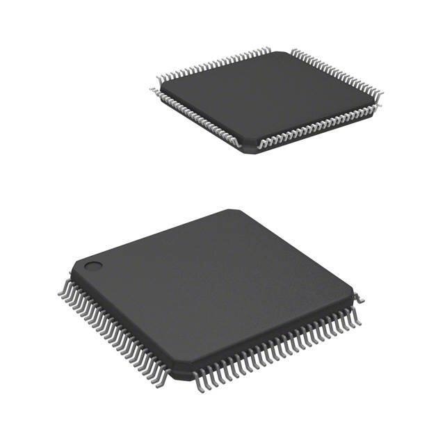


 工商网监
湘ICP备2023018690号
工商网监
湘ICP备2023018690号
