STM32F410x8 STM32F410xB
Arm®-Cortex®-M4 32b MCU+FPU, 125 DMIPS, 128KB Flash,
32KB RAM, 9 TIMs, 1 ADC, 1 DAC, 1 LPTIM, 9 comm. interfaces
Datasheet - production data
Features
&"'!
• Dynamic Efficiency Line with eBAM (enhanced
Batch Acquisition Mode)
– 1.7 V to 3.6 V power supply
– -40 °C to 85/105/125 °C temperature range
• Core: Arm® 32-bit Cortex®-M4 CPU with FPU,
Adaptive real-time accelerator (ART
Accelerator™) allowing 0-wait state execution
from Flash memory, frequency up to 100 MHz,
memory protection unit,
125 DMIPS/1.25 DMIPS/MHz (Dhrystone 2.1),
and DSP instructions
• Memories
– Up to 128 Kbytes of Flash memory
– 512 bytes of OTP memory
– 32 Kbytes of SRAM
• Clock, reset and supply management
– 1.7 V to 3.6 V application supply and I/Os
– POR, PDR, PVD and BOR
– 4-to-26 MHz crystal oscillator
– Internal 16 MHz factory-trimmed RC
– 32 kHz oscillator for RTC with calibration
– Internal 32 kHz RC with calibration
• Power consumption
– Run: 89 µA/MHz (peripheral off)
– Stop (Flash in Stop mode, fast wakeup
time): 40 µA Typ @ 25 °C; 49 µA max
@25 °C
– Stop (Flash in Deep power down mode,
slow wakeup time): down to 6 µA @ 25 °C;
14 µA max @25 °C
– Standby: 2.4 µA @25 °C / 1.7 V without
RTC; 12 µA @85 °C @1.7 V
– VBAT supply for RTC: 1 µA @25 °C
• 1×12-bit, 2.4 MSPS ADC: up to 16 channels
WLCSP36
LQFP48 (7x7mm)
(2.553x2.579mm) LQFP64 (10×10mm)
• Debug mode
– Serial wire debug (SWD) & JTAG
interfaces
– Cortex® -M4 Embedded Trace Macrocell™
• Up to 50 I/O ports with interrupt capability
– Up to 45 fast I/Os up to 100 MHz
– Up to 49 5 V-tolerant I/Os
• Up to 9 communication interfaces
– Up to 3x I2C interfaces (SMBus/PMBus)
including 1x I2C Fast-mode at 1 MHz
– Up to 3 USARTs (2 x 12.5 Mbit/s,
1 x 6.25 Mbit/s), ISO 7816 interface, LIN,
IrDA, modem control)
– Up to 3 SPI/I2Ss (up to 50 Mbit/s SPI or
I2S audio protocol)
• True random number generator
• CRC calculation unit
• 96-bit unique ID
• RTC: subsecond accuracy, hardware calendar
• All packages are ECOPACK®2
Table 1. Device summary
• General-purpose DMA: 16-stream DMA
controllers with FIFOs and burst support
• Up to 9 timers
– One low-power timer (available in Stop
mode)
This is information on a product in full production.
UFBGA64
(5x5mm)
– One 16-bit advanced motor-control timer
– Three 16-bit general purpose timers
– One 32-bit timer up to 100 MHz with up to
four IC/OC/PWM or pulse counter and
quadrature (incremental) encoder input
– Two watchdog timers (independent
window)
– SysTick timer.
• 1×12-bit D/A converter
December 2017
UFQFPN48
(7×7mm)
Reference
Part number
STM32F410x8
STM32F410T8, STM32F410C8,
STM32F410R8
STM32F410xB
STM32F410TB, STM32F410CB,
STM32F410RB
DocID028094 Rev 6
1/143
www.st.com
�Contents
STM32F410x8/B
Contents
1
Introduction . . . . . . . . . . . . . . . . . . . . . . . . . . . . . . . . . . . . . . . . . . . . . . . 11
2
Description . . . . . . . . . . . . . . . . . . . . . . . . . . . . . . . . . . . . . . . . . . . . . . . . 12
2.1
3
Compatibility with STM32F4 series . . . . . . . . . . . . . . . . . . . . . . . . . . . . . 14
Functional overview . . . . . . . . . . . . . . . . . . . . . . . . . . . . . . . . . . . . . . . . 16
3.1
Arm® Cortex®-M4 with FPU core with embedded Flash and SRAM . . . . 16
3.2
Adaptive real-time memory accelerator (ART Accelerator™) . . . . . . . . . 16
3.3
Batch Acquisition mode (BAM) . . . . . . . . . . . . . . . . . . . . . . . . . . . . . . . . . 16
3.4
Memory protection unit . . . . . . . . . . . . . . . . . . . . . . . . . . . . . . . . . . . . . . . 17
3.5
Embedded Flash memory . . . . . . . . . . . . . . . . . . . . . . . . . . . . . . . . . . . . 17
3.6
CRC (cyclic redundancy check) calculation unit . . . . . . . . . . . . . . . . . . . 17
3.7
Embedded SRAM . . . . . . . . . . . . . . . . . . . . . . . . . . . . . . . . . . . . . . . . . . . 17
3.8
Multi-AHB bus matrix . . . . . . . . . . . . . . . . . . . . . . . . . . . . . . . . . . . . . . . . 18
3.9
DMA controller (DMA) . . . . . . . . . . . . . . . . . . . . . . . . . . . . . . . . . . . . . . . 18
3.10
Nested vectored interrupt controller (NVIC) . . . . . . . . . . . . . . . . . . . . . . . 19
3.11
External interrupt/event controller (EXTI) . . . . . . . . . . . . . . . . . . . . . . . . . 19
3.12
Clocks and startup . . . . . . . . . . . . . . . . . . . . . . . . . . . . . . . . . . . . . . . . . . 19
3.13
Boot modes . . . . . . . . . . . . . . . . . . . . . . . . . . . . . . . . . . . . . . . . . . . . . . . 20
3.14
Power supply schemes . . . . . . . . . . . . . . . . . . . . . . . . . . . . . . . . . . . . . . 20
3.15
Power supply supervisor . . . . . . . . . . . . . . . . . . . . . . . . . . . . . . . . . . . . . 21
3.16
3.15.1
Internal reset ON . . . . . . . . . . . . . . . . . . . . . . . . . . . . . . . . . . . . . . . . . . 21
3.15.2
Internal reset OFF . . . . . . . . . . . . . . . . . . . . . . . . . . . . . . . . . . . . . . . . . 21
Voltage regulator . . . . . . . . . . . . . . . . . . . . . . . . . . . . . . . . . . . . . . . . . . . 22
3.16.1
2/143
Internal power supply supervisor availability . . . . . . . . . . . . . . . . . . . . . 22
3.17
Real-time clock (RTC) and backup registers . . . . . . . . . . . . . . . . . . . . . . 23
3.18
Low-power modes . . . . . . . . . . . . . . . . . . . . . . . . . . . . . . . . . . . . . . . . . . 23
3.19
VBAT operation . . . . . . . . . . . . . . . . . . . . . . . . . . . . . . . . . . . . . . . . . . . . . 24
3.20
Timers and watchdogs . . . . . . . . . . . . . . . . . . . . . . . . . . . . . . . . . . . . . . . 24
3.20.1
Advanced-control timers (TIM1) . . . . . . . . . . . . . . . . . . . . . . . . . . . . . . 26
3.20.2
General-purpose timers (TIM5, TIM9 and TIM11) . . . . . . . . . . . . . . . . . 26
3.20.3
Basic timer (TIM6) . . . . . . . . . . . . . . . . . . . . . . . . . . . . . . . . . . . . . . . . . 26
DocID028094 Rev 6
�STM32F410x8/B
Contents
3.20.4
Low-power timer (LPTIM1) . . . . . . . . . . . . . . . . . . . . . . . . . . . . . . . . . . 27
3.20.5
Independent watchdog . . . . . . . . . . . . . . . . . . . . . . . . . . . . . . . . . . . . . 27
3.20.6
Window watchdog . . . . . . . . . . . . . . . . . . . . . . . . . . . . . . . . . . . . . . . . . 27
3.20.7
SysTick timer . . . . . . . . . . . . . . . . . . . . . . . . . . . . . . . . . . . . . . . . . . . . . 27
3.21
Inter-integrated circuit interface (I2C) . . . . . . . . . . . . . . . . . . . . . . . . . . . . 28
3.22
Universal synchronous/asynchronous receiver transmitters (USART) . . 28
3.23
Serial peripheral interface (SPI) . . . . . . . . . . . . . . . . . . . . . . . . . . . . . . . . 29
3.24
Inter-integrated sound (I2S) . . . . . . . . . . . . . . . . . . . . . . . . . . . . . . . . . . . 29
3.25
Random number generator (RNG) . . . . . . . . . . . . . . . . . . . . . . . . . . . . . . 29
3.26
General-purpose input/outputs (GPIOs) . . . . . . . . . . . . . . . . . . . . . . . . . . 30
3.27
Analog-to-digital converter (ADC) . . . . . . . . . . . . . . . . . . . . . . . . . . . . . . 30
3.28
Temperature sensor . . . . . . . . . . . . . . . . . . . . . . . . . . . . . . . . . . . . . . . . . 30
3.29
Digital-to-analog converter (DAC) . . . . . . . . . . . . . . . . . . . . . . . . . . . . . . 30
3.30
Serial wire JTAG debug port (SWJ-DP) . . . . . . . . . . . . . . . . . . . . . . . . . . 31
3.31
Embedded Trace Macrocell™ . . . . . . . . . . . . . . . . . . . . . . . . . . . . . . . . . 31
4
Pinouts and pin description . . . . . . . . . . . . . . . . . . . . . . . . . . . . . . . . . . 32
5
Memory mapping . . . . . . . . . . . . . . . . . . . . . . . . . . . . . . . . . . . . . . . . . . . 44
6
Electrical characteristics . . . . . . . . . . . . . . . . . . . . . . . . . . . . . . . . . . . . 48
6.1
Parameter conditions . . . . . . . . . . . . . . . . . . . . . . . . . . . . . . . . . . . . . . . . 48
6.1.1
Minimum and maximum values . . . . . . . . . . . . . . . . . . . . . . . . . . . . . . . 48
6.1.2
Typical values . . . . . . . . . . . . . . . . . . . . . . . . . . . . . . . . . . . . . . . . . . . . 48
6.1.3
Typical curves . . . . . . . . . . . . . . . . . . . . . . . . . . . . . . . . . . . . . . . . . . . . 48
6.1.4
Loading capacitor . . . . . . . . . . . . . . . . . . . . . . . . . . . . . . . . . . . . . . . . . 48
6.1.5
Pin input voltage . . . . . . . . . . . . . . . . . . . . . . . . . . . . . . . . . . . . . . . . . . 49
6.1.6
Power supply scheme . . . . . . . . . . . . . . . . . . . . . . . . . . . . . . . . . . . . . . 50
6.1.7
Current consumption measurement . . . . . . . . . . . . . . . . . . . . . . . . . . . 51
6.2
Absolute maximum ratings . . . . . . . . . . . . . . . . . . . . . . . . . . . . . . . . . . . . 51
6.3
Operating conditions . . . . . . . . . . . . . . . . . . . . . . . . . . . . . . . . . . . . . . . . 53
6.3.1
General operating conditions . . . . . . . . . . . . . . . . . . . . . . . . . . . . . . . . . 53
6.3.2
VCAP_1 external capacitor . . . . . . . . . . . . . . . . . . . . . . . . . . . . . . . . . . 56
6.3.3
Operating conditions at power-up/power-down (regulator ON) . . . . . . . 56
6.3.4
Operating conditions at power-up / power-down (regulator OFF) . . . . . 56
6.3.5
Embedded reset and power control block characteristics . . . . . . . . . . . 57
DocID028094 Rev 6
3/143
5
�Contents
7
STM32F410x8/B
6.3.6
Supply current characteristics . . . . . . . . . . . . . . . . . . . . . . . . . . . . . . . . 58
6.3.7
Wakeup time from low-power modes . . . . . . . . . . . . . . . . . . . . . . . . . . . 77
6.3.8
External clock source characteristics . . . . . . . . . . . . . . . . . . . . . . . . . . . 78
6.3.9
Internal clock source characteristics . . . . . . . . . . . . . . . . . . . . . . . . . . . 83
6.3.10
PLL characteristics . . . . . . . . . . . . . . . . . . . . . . . . . . . . . . . . . . . . . . . . 84
6.3.11
PLL spread spectrum clock generation (SSCG) characteristics . . . . . . 86
6.3.12
Memory characteristics . . . . . . . . . . . . . . . . . . . . . . . . . . . . . . . . . . . . . 87
6.3.13
EMC characteristics . . . . . . . . . . . . . . . . . . . . . . . . . . . . . . . . . . . . . . . . 89
6.3.14
Absolute maximum ratings (electrical sensitivity) . . . . . . . . . . . . . . . . . 91
6.3.15
I/O current injection characteristics . . . . . . . . . . . . . . . . . . . . . . . . . . . . 91
6.3.16
I/O port characteristics . . . . . . . . . . . . . . . . . . . . . . . . . . . . . . . . . . . . . . 92
6.3.17
NRST pin characteristics . . . . . . . . . . . . . . . . . . . . . . . . . . . . . . . . . . . . 97
6.3.18
TIM timer characteristics . . . . . . . . . . . . . . . . . . . . . . . . . . . . . . . . . . . . 98
6.3.19
Communications interfaces . . . . . . . . . . . . . . . . . . . . . . . . . . . . . . . . . . 99
6.3.20
12-bit ADC characteristics . . . . . . . . . . . . . . . . . . . . . . . . . . . . . . . . . . 109
6.3.21
Temperature sensor characteristics . . . . . . . . . . . . . . . . . . . . . . . . . . . 114
6.3.22
VBAT monitoring characteristics . . . . . . . . . . . . . . . . . . . . . . . . . . . . . . 115
6.3.23
Embedded reference voltage . . . . . . . . . . . . . . . . . . . . . . . . . . . . . . . . 115
6.3.24
DAC electrical characteristics . . . . . . . . . . . . . . . . . . . . . . . . . . . . . . . 116
6.3.25
RTC characteristics . . . . . . . . . . . . . . . . . . . . . . . . . . . . . . . . . . . . . . . 118
Package information . . . . . . . . . . . . . . . . . . . . . . . . . . . . . . . . . . . . . . . 119
7.1
WLCSP36 package information . . . . . . . . . . . . . . . . . . . . . . . . . . . . . . . .119
7.2
UFQFPN48 package information . . . . . . . . . . . . . . . . . . . . . . . . . . . . . . 122
7.3
LQFP48 package information . . . . . . . . . . . . . . . . . . . . . . . . . . . . . . . . . 125
7.4
LQFP64 package information . . . . . . . . . . . . . . . . . . . . . . . . . . . . . . . . . 129
7.5
UFBGA64 package information . . . . . . . . . . . . . . . . . . . . . . . . . . . . . . . 132
7.6
Thermal characteristics . . . . . . . . . . . . . . . . . . . . . . . . . . . . . . . . . . . . . 135
7.6.1
8
Reference document . . . . . . . . . . . . . . . . . . . . . . . . . . . . . . . . . . . . . . 135
Part numbering . . . . . . . . . . . . . . . . . . . . . . . . . . . . . . . . . . . . . . . . . . . 136
Appendix A Recommendations when using the internal reset OFF . . . . . . . . 137
A.1
Operating conditions . . . . . . . . . . . . . . . . . . . . . . . . . . . . . . . . . . . . . . . . 137
Appendix B Application block diagrams . . . . . . . . . . . . . . . . . . . . . . . . . . . . . . 138
B.1
4/143
Sensor Hub application example. . . . . . . . . . . . . . . . . . . . . . . . . . . . . . . 138
DocID028094 Rev 6
�STM32F410x8/B
Contents
B.2
Batch Acquisition Mode (BAM) example . . . . . . . . . . . . . . . . . . . . . . . . . 139
Revision history . . . . . . . . . . . . . . . . . . . . . . . . . . . . . . . . . . . . . . . . . . . . . . . . . . . 140
DocID028094 Rev 6
5/143
5
�List of tables
STM32F410x8/B
List of tables
Table 1.
Table 2.
Table 3.
Table 4.
Table 5.
Table 6.
Table 7.
Table 8.
Table 9.
Table 10.
Table 11.
Table 12.
Table 13.
Table 14.
Table 15.
Table 16.
Table 17.
Table 18.
Table 19.
Table 20.
Table 21.
Table 22.
Table 23.
Table 24.
Table 25.
Table 26.
Table 27.
Table 28.
Table 29.
Table 30.
Table 31.
Table 32.
Table 33.
Table 34.
Table 35.
Table 36.
Table 37.
Table 38.
Table 39.
Table 40.
6/143
Device summary . . . . . . . . . . . . . . . . . . . . . . . . . . . . . . . . . . . . . . . . . . . . . . . . . . . . . . . . . . 1
STM32F410x8/B features and peripheral counts . . . . . . . . . . . . . . . . . . . . . . . . . . . . . . . . 13
Embedded bootloader interfaces . . . . . . . . . . . . . . . . . . . . . . . . . . . . . . . . . . . . . . . . . . . . 20
Regulator ON/OFF and internal power supply supervisor availability. . . . . . . . . . . . . . . . . 22
Timer feature comparison . . . . . . . . . . . . . . . . . . . . . . . . . . . . . . . . . . . . . . . . . . . . . . . . . . 25
Comparison of I2C analog and digital filters . . . . . . . . . . . . . . . . . . . . . . . . . . . . . . . . . . . . 28
USART feature comparison . . . . . . . . . . . . . . . . . . . . . . . . . . . . . . . . . . . . . . . . . . . . . . . . 29
Legend/abbreviations used in the pinout table . . . . . . . . . . . . . . . . . . . . . . . . . . . . . . . . . . 34
STM32F410x8/B pin definitions . . . . . . . . . . . . . . . . . . . . . . . . . . . . . . . . . . . . . . . . . . . . . 35
Alternate function mapping . . . . . . . . . . . . . . . . . . . . . . . . . . . . . . . . . . . . . . . . . . . . . . . . . 41
STM32F410x8/B register boundary addresses . . . . . . . . . . . . . . . . . . . . . . . . . . . . . . . . . 45
Voltage characteristics . . . . . . . . . . . . . . . . . . . . . . . . . . . . . . . . . . . . . . . . . . . . . . . . . . . . 51
Current characteristics . . . . . . . . . . . . . . . . . . . . . . . . . . . . . . . . . . . . . . . . . . . . . . . . . . . . 52
Thermal characteristics. . . . . . . . . . . . . . . . . . . . . . . . . . . . . . . . . . . . . . . . . . . . . . . . . . . . 52
General operating conditions . . . . . . . . . . . . . . . . . . . . . . . . . . . . . . . . . . . . . . . . . . . . . . . 53
Features depending on the operating power supply range . . . . . . . . . . . . . . . . . . . . . . . . 55
VCAP_1 operating conditions . . . . . . . . . . . . . . . . . . . . . . . . . . . . . . . . . . . . . . . . . . . . . . . 56
Operating conditions at power-up / power-down (regulator ON) . . . . . . . . . . . . . . . . . . . . 56
Operating conditions at power-up / power-down (regulator OFF). . . . . . . . . . . . . . . . . . . . 56
Embedded reset and power control block characteristics. . . . . . . . . . . . . . . . . . . . . . . . . . 57
Typical and maximum current consumption, code with data processing (ART
accelerator disabled) running from SRAM - VDD = 1.7 V . . . . . . . . . . . . . . . . . . . . . . . . . . 59
Typical and maximum current consumption, code with data processing (ART
accelerator disabled) running from SRAM - VDD = 3.6 V . . . . . . . . . . . . . . . . . . . . . . . . . . 60
Typical and maximum current consumption in run mode, code with data processing
(ART accelerator enabled except prefetch) running from Flash memory- VDD = 1.7 V . . . 61
Typical and maximum current consumption in run mode, code with data processing
(ART accelerator enabled except prefetch) running from Flash memory - VDD = 3.6 V . . 62
Typical and maximum current consumption in run mode, code with data processing
(ART accelerator disabled) running from Flash memory - VDD = 3.6 V. . . . . . . . . . . . . . . 63
Typical and maximum current consumption in run mode, code with data processing
(ART accelerator disabled) running from Flash memory - VDD = 1.7 V. . . . . . . . . . . . . . . 64
Typical and maximum current consumption in run mode, code with data processing
(ART accelerator enabled with prefetch) running from Flash memory - VDD = 3.6 V . . . . . 65
Typical and maximum current consumption in Sleep mode - VDD = 3.6 V . . . . . . . . . . . . . 66
Typical and maximum current consumption in Sleep mode - VDD = 1.7 V . . . . . . . . . . . . . 68
Typical and maximum current consumptions in Stop mode - VDD = 1.7 V . . . . . . . . . . . . . 70
Typical and maximum current consumption in Stop mode - VDD=3.6 V. . . . . . . . . . . . . . . 70
Typical and maximum current consumption in Standby mode - VDD= 1.7 V . . . . . . . . . . . 70
Typical and maximum current consumption in Standby mode - VDD= 3.6 V . . . . . . . . . . . 71
Typical and maximum current consumptions in VBAT mode
(LSE and RTC ON, LSE low- drive mode) . . . . . . . . . . . . . . . . . . . . . . . . . . . . . . . . . . . . . 71
Switching output I/O current consumption . . . . . . . . . . . . . . . . . . . . . . . . . . . . . . . . . . . . . 74
Peripheral current consumption . . . . . . . . . . . . . . . . . . . . . . . . . . . . . . . . . . . . . . . . . . . . . 75
Low-power mode wakeup timings . . . . . . . . . . . . . . . . . . . . . . . . . . . . . . . . . . . . . . . . . . . 78
High-speed external user clock characteristics. . . . . . . . . . . . . . . . . . . . . . . . . . . . . . . . . . 79
Low-speed external user clock characteristics . . . . . . . . . . . . . . . . . . . . . . . . . . . . . . . . . . 79
HSE 4-26 MHz oscillator characteristics. . . . . . . . . . . . . . . . . . . . . . . . . . . . . . . . . . . . . . . 81
DocID028094 Rev 6
�STM32F410x8/B
Table 41.
Table 42.
Table 43.
Table 44.
Table 45.
Table 46.
Table 47.
Table 48.
Table 49.
Table 50.
Table 51.
Table 52.
Table 53.
Table 54.
Table 55.
Table 56.
Table 57.
Table 58.
Table 59.
Table 60.
Table 61.
Table 62.
Table 63.
Table 64.
Table 65.
Table 66.
Table 67.
Table 68.
Table 69.
Table 70.
Table 71.
Table 72.
Table 73.
Table 74.
Table 75.
Table 76.
Table 77.
Table 78.
Table 79.
Table 80.
Table 81.
Table 82.
Table 83.
Table 84.
Table 85.
Table 86.
Table 87.
Table 88.
List of tables
LSE oscillator characteristics (fLSE = 32.768 kHz) . . . . . . . . . . . . . . . . . . . . . . . . . . . . . . . 82
HSI oscillator characteristics . . . . . . . . . . . . . . . . . . . . . . . . . . . . . . . . . . . . . . . . . . . . . . . 83
LSI oscillator characteristics . . . . . . . . . . . . . . . . . . . . . . . . . . . . . . . . . . . . . . . . . . . . . . . 84
Main PLL characteristics. . . . . . . . . . . . . . . . . . . . . . . . . . . . . . . . . . . . . . . . . . . . . . . . . . . 84
SSCG parameter constraints . . . . . . . . . . . . . . . . . . . . . . . . . . . . . . . . . . . . . . . . . . . . . . . 86
Flash memory characteristics . . . . . . . . . . . . . . . . . . . . . . . . . . . . . . . . . . . . . . . . . . . . . . . 87
Flash memory programming . . . . . . . . . . . . . . . . . . . . . . . . . . . . . . . . . . . . . . . . . . . . . . . . 88
Flash memory programming with VPP voltage . . . . . . . . . . . . . . . . . . . . . . . . . . . . . . . . . . 88
Flash memory endurance and data retention . . . . . . . . . . . . . . . . . . . . . . . . . . . . . . . . . . . 89
EMS characteristics . . . . . . . . . . . . . . . . . . . . . . . . . . . . . . . . . . . . . . . . . . . . . . . . . . . . . . 89
EMI characteristics for LQFP64 . . . . . . . . . . . . . . . . . . . . . . . . . . . . . . . . . . . . . . . . . . . . . 90
ESD absolute maximum ratings . . . . . . . . . . . . . . . . . . . . . . . . . . . . . . . . . . . . . . . . . . . . . 91
Electrical sensitivities . . . . . . . . . . . . . . . . . . . . . . . . . . . . . . . . . . . . . . . . . . . . . . . . . . . . . 91
I/O current injection susceptibility . . . . . . . . . . . . . . . . . . . . . . . . . . . . . . . . . . . . . . . . . . . . 92
I/O static characteristics . . . . . . . . . . . . . . . . . . . . . . . . . . . . . . . . . . . . . . . . . . . . . . . . . . . 92
Output voltage characteristics . . . . . . . . . . . . . . . . . . . . . . . . . . . . . . . . . . . . . . . . . . . . . . 95
I/O AC characteristics . . . . . . . . . . . . . . . . . . . . . . . . . . . . . . . . . . . . . . . . . . . . . . . . . . . . . 95
NRST pin characteristics . . . . . . . . . . . . . . . . . . . . . . . . . . . . . . . . . . . . . . . . . . . . . . . . . . 97
TIMx characteristics . . . . . . . . . . . . . . . . . . . . . . . . . . . . . . . . . . . . . . . . . . . . . . . . . . . . . . 98
I2C characteristics. . . . . . . . . . . . . . . . . . . . . . . . . . . . . . . . . . . . . . . . . . . . . . . . . . . . . . . . 99
SCL frequency (fPCLK1= 50 MHz, VDD = VDD_I2C = 3.3 V) . . . . . . . . . . . . . . . . . . . . . . . . 100
SCL frequency (fPCLK1= 42 MHz.,VDD = VDD_I2C = 3.3 V) . . . . . . . . . . . . . . . . . . . . . . . . 101
FMPI2C characteristics . . . . . . . . . . . . . . . . . . . . . . . . . . . . . . . . . . . . . . . . . . . . . . . . . . . 102
SPI dynamic characteristics . . . . . . . . . . . . . . . . . . . . . . . . . . . . . . . . . . . . . . . . . . . . . . . 104
I2S dynamic characteristics . . . . . . . . . . . . . . . . . . . . . . . . . . . . . . . . . . . . . . . . . . . . . . . 107
ADC characteristics . . . . . . . . . . . . . . . . . . . . . . . . . . . . . . . . . . . . . . . . . . . . . . . . . . . . . 109
ADC accuracy at fADC = 18 MHz . . . . . . . . . . . . . . . . . . . . . . . . . . . . . . . . . . . . . . . . . . . 110
ADC accuracy at fADC = 30 MHz . . . . . . . . . . . . . . . . . . . . . . . . . . . . . . . . . . . . . . . . . . . 111
ADC accuracy at fADC = 36 MHz . . . . . . . . . . . . . . . . . . . . . . . . . . . . . . . . . . . . . . . . . . . 111
ADC dynamic accuracy at fADC = 18 MHz - limited test conditions . . . . . . . . . . . . . . . . . 111
ADC dynamic accuracy at fADC = 36 MHz - limited test conditions . . . . . . . . . . . . . . . . . 111
Temperature sensor characteristics . . . . . . . . . . . . . . . . . . . . . . . . . . . . . . . . . . . . . . . . . 114
Temperature sensor calibration values. . . . . . . . . . . . . . . . . . . . . . . . . . . . . . . . . . . . . . . 114
VBAT monitoring characteristics . . . . . . . . . . . . . . . . . . . . . . . . . . . . . . . . . . . . . . . . . . . . 115
Embedded internal reference voltage . . . . . . . . . . . . . . . . . . . . . . . . . . . . . . . . . . . . . . . . 115
Internal reference voltage calibration values . . . . . . . . . . . . . . . . . . . . . . . . . . . . . . . . . . 115
DAC characteristics . . . . . . . . . . . . . . . . . . . . . . . . . . . . . . . . . . . . . . . . . . . . . . . . . . . . . 116
RTC characteristics . . . . . . . . . . . . . . . . . . . . . . . . . . . . . . . . . . . . . . . . . . . . . . . . . . . . . 118
WLCSP36 - 36-pin, 2.553 x 2.579 mm, 0.4 mm pitch wafer level chip scale
package mechanical data . . . . . . . . . . . . . . . . . . . . . . . . . . . . . . . . . . . . . . . . . . . . . . . . . 120
WLCSP36 recommended PCB design rules (0.4 mm pitch) . . . . . . . . . . . . . . . . . . . . . . 121
UFQFPN48 - 48-lead, 7x7 mm, 0.5 mm pitch, ultra thin fine pitch quad flat
package mechanical data . . . . . . . . . . . . . . . . . . . . . . . . . . . . . . . . . . . . . . . . . . . . . . . . . 123
LQFP48 - 48-pin, 7 x 7 mm low-profile quad flat package
mechanical data . . . . . . . . . . . . . . . . . . . . . . . . . . . . . . . . . . . . . . . . . . . . . . . . . . . . . . . . 126
LQFP64 - 64-pin, 10 x 10 mm low-profile quad flat package mechanical data. . . . . . . . . 130
UFBGA64 – 64-ball, 5 x 5 mm, 0.5 mm pitch ultra profile fine pitch ball grid array
package mechanical data . . . . . . . . . . . . . . . . . . . . . . . . . . . . . . . . . . . . . . . . . . . . . . . . . 132
UFBGA64 recommended PCB design rules (0.5 mm pitch BGA) . . . . . . . . . . . . . . . . . . 133
Package thermal characteristics . . . . . . . . . . . . . . . . . . . . . . . . . . . . . . . . . . . . . . . . . . . . 135
Ordering information scheme . . . . . . . . . . . . . . . . . . . . . . . . . . . . . . . . . . . . . . . . . . . . . . 136
Limitations depending on the operating power supply range . . . . . . . . . . . . . . . . . . . . . . 137
DocID028094 Rev 6
7/143
8
�List of tables
Table 89.
8/143
STM32F410x8/B
Document revision history . . . . . . . . . . . . . . . . . . . . . . . . . . . . . . . . . . . . . . . . . . . . . . . . 140
DocID028094 Rev 6
�STM32F410x8/B
List of figures
List of figures
Figure 1.
Figure 2.
Figure 3.
Figure 4.
Figure 5.
Figure 6.
Figure 7.
Figure 8.
Figure 9.
Figure 10.
Figure 11.
Figure 12.
Figure 13.
Figure 14.
Figure 15.
Figure 16.
Figure 17.
Figure 18.
Figure 19.
Figure 20.
Figure 21.
Figure 22.
Figure 23.
Figure 24.
Figure 25.
Figure 26.
Figure 27.
Figure 28.
Figure 29.
Figure 30.
Figure 31.
Figure 32.
Figure 33.
Figure 34.
Figure 35.
Figure 36.
Figure 37.
Figure 38.
Figure 39.
Figure 40.
Figure 41.
Figure 42.
Figure 43.
Figure 44.
Compatible board design for LQFP64 package . . . . . . . . . . . . . . . . . . . . . . . . . . . . . . . . . 14
STM32F410x8/B block diagram . . . . . . . . . . . . . . . . . . . . . . . . . . . . . . . . . . . . . . . . . . . . . 15
Multi-AHB matrix . . . . . . . . . . . . . . . . . . . . . . . . . . . . . . . . . . . . . . . . . . . . . . . . . . . . . . . . . 18
Power supply supervisor interconnection with internal reset OFF . . . . . . . . . . . . . . . . . . . 21
LQFP48 pinout . . . . . . . . . . . . . . . . . . . . . . . . . . . . . . . . . . . . . . . . . . . . . . . . . . . . . . . . . . 32
LQFP64 pinout . . . . . . . . . . . . . . . . . . . . . . . . . . . . . . . . . . . . . . . . . . . . . . . . . . . . . . . . . . 32
UFQFPN48 pinout . . . . . . . . . . . . . . . . . . . . . . . . . . . . . . . . . . . . . . . . . . . . . . . . . . . . . . . 33
UFBGA64 pinout. . . . . . . . . . . . . . . . . . . . . . . . . . . . . . . . . . . . . . . . . . . . . . . . . . . . . . . . . 33
WLCSP36 pinout . . . . . . . . . . . . . . . . . . . . . . . . . . . . . . . . . . . . . . . . . . . . . . . . . . . . . . . . 34
Memory map . . . . . . . . . . . . . . . . . . . . . . . . . . . . . . . . . . . . . . . . . . . . . . . . . . . . . . . . . . . . 44
Pin loading conditions . . . . . . . . . . . . . . . . . . . . . . . . . . . . . . . . . . . . . . . . . . . . . . . . . . . . . 48
Input voltage measurement . . . . . . . . . . . . . . . . . . . . . . . . . . . . . . . . . . . . . . . . . . . . . . . . 49
Power supply scheme. . . . . . . . . . . . . . . . . . . . . . . . . . . . . . . . . . . . . . . . . . . . . . . . . . . . . 50
Current consumption measurement scheme . . . . . . . . . . . . . . . . . . . . . . . . . . . . . . . . . . . 51
External capacitor CEXT . . . . . . . . . . . . . . . . . . . . . . . . . . . . . . . . . . . . . . . . . . . . . . . . . . . 56
Typical VBAT current consumption (LSE and RTC ON/LSE oscillator
in “low power” mode selection . . . . . . . . . . . . . . . . . . . . . . . . . . . . . . . . . . . . . . . . . . . . . . 72
Typical VBAT current consumption (LSE and RTC ON/LSE oscillator
in “high-drive” mode selection) . . . . . . . . . . . . . . . . . . . . . . . . . . . . . . . . . . . . . . . . . . . . . . 72
Low-power mode wakeup . . . . . . . . . . . . . . . . . . . . . . . . . . . . . . . . . . . . . . . . . . . . . . . . . . 77
High-speed external clock source AC timing diagram . . . . . . . . . . . . . . . . . . . . . . . . . . . . 80
Low-speed external clock source AC timing diagram . . . . . . . . . . . . . . . . . . . . . . . . . . . . . 80
Typical application with an 8 MHz crystal . . . . . . . . . . . . . . . . . . . . . . . . . . . . . . . . . . . . . . 81
Typical application with a 32.768 kHz crystal . . . . . . . . . . . . . . . . . . . . . . . . . . . . . . . . . . . 82
ACCHSI versus temperature . . . . . . . . . . . . . . . . . . . . . . . . . . . . . . . . . . . . . . . . . . . . . . . . 83
ACCLSI versus temperature . . . . . . . . . . . . . . . . . . . . . . . . . . . . . . . . . . . . . . . . . . . . . . . . 84
PLL output clock waveforms in center spread mode . . . . . . . . . . . . . . . . . . . . . . . . . . . . . 87
PLL output clock waveforms in down spread mode . . . . . . . . . . . . . . . . . . . . . . . . . . . . . . 87
FT/TC I/O input characteristics . . . . . . . . . . . . . . . . . . . . . . . . . . . . . . . . . . . . . . . . . . . . . . 94
I/O AC characteristics definition . . . . . . . . . . . . . . . . . . . . . . . . . . . . . . . . . . . . . . . . . . . . . 97
Recommended NRST pin protection . . . . . . . . . . . . . . . . . . . . . . . . . . . . . . . . . . . . . . . . . 98
I2C bus AC waveforms and measurement circuit . . . . . . . . . . . . . . . . . . . . . . . . . . . . . . . 100
FMPI2C timing diagram and measurement circuit . . . . . . . . . . . . . . . . . . . . . . . . . . . . . . 103
SPI timing diagram - slave mode and CPHA = 0 . . . . . . . . . . . . . . . . . . . . . . . . . . . . . . . 105
SPI timing diagram - slave mode and CPHA = 1(1) . . . . . . . . . . . . . . . . . . . . . . . . . . . . . 106
SPI timing diagram - master mode(1) . . . . . . . . . . . . . . . . . . . . . . . . . . . . . . . . . . . . . . . . 106
I2S slave timing diagram (Philips protocol)(1) . . . . . . . . . . . . . . . . . . . . . . . . . . . . . . . . . . 108
I2S master timing diagram (Philips protocol)(1) . . . . . . . . . . . . . . . . . . . . . . . . . . . . . . . . . 108
ADC accuracy characteristics . . . . . . . . . . . . . . . . . . . . . . . . . . . . . . . . . . . . . . . . . . . . . . 112
Typical connection diagram using the ADC . . . . . . . . . . . . . . . . . . . . . . . . . . . . . . . . . . . 113
Power supply and reference decoupling. . . . . . . . . . . . . . . . . . . . . . . . . . . . . . . . . . . . . . 114
12-bit buffered/non-buffered DAC. . . . . . . . . . . . . . . . . . . . . . . . . . . . . . . . . . . . . . . . . . . 118
WLCSP36 - 36-pin, 2.553 x 2.579 mm, 0.4 mm pitch wafer level chip scale
package outline. . . . . . . . . . . . . . . . . . . . . . . . . . . . . . . . . . . . . . . . . . . . . . . . . . . . . . . . . 119
WLCSP36 - 36-pin, 2.553 x 2.579 mm, 0.4 mm pitch wafer level chip scale
package recommended footprint . . . . . . . . . . . . . . . . . . . . . . . . . . . . . . . . . . . . . . . . . . . 120
WLCSP36 marking example (package top view) . . . . . . . . . . . . . . . . . . . . . . . . . . . . . . . 121
UFQFPN48 - 48-lead, 7x7 mm, 0.5 mm pitch, ultra thin fine pitch quad flat
DocID028094 Rev 6
9/143
10
�List of figures
Figure 45.
Figure 46.
Figure 47.
Figure 48.
Figure 49.
Figure 50.
Figure 51.
Figure 52.
Figure 53.
Figure 54.
Figure 55.
Figure 56.
Figure 57.
Figure 58.
10/143
STM32F410x8/B
package outline. . . . . . . . . . . . . . . . . . . . . . . . . . . . . . . . . . . . . . . . . . . . . . . . . . . . . . . . . 122
UFQFPN48 recommended footprint . . . . . . . . . . . . . . . . . . . . . . . . . . . . . . . . . . . . . . . . . 123
UFQFPN48 marking example (package top view) . . . . . . . . . . . . . . . . . . . . . . . . . . . . . . 124
LQFP48 - 48-pin, 7 x 7 mm low-profile quad flat package outline . . . . . . . . . . . . . . . . . . 125
LQFP48 - 48-pin, 7 x 7 mm low-profile quad flat package
recommended footprint . . . . . . . . . . . . . . . . . . . . . . . . . . . . . . . . . . . . . . . . . . . . . . . . . . . 127
LQFP48 marking example (package top view) . . . . . . . . . . . . . . . . . . . . . . . . . . . . . . . . 128
LQFP64 - 64-pin, 10 x 10 mm low-profile quad flat package outline . . . . . . . . . . . . . . . . 129
LQFP64 recommended footprint . . . . . . . . . . . . . . . . . . . . . . . . . . . . . . . . . . . . . . . . . . . 130
LQFP64 marking example (package top view) . . . . . . . . . . . . . . . . . . . . . . . . . . . . . . . . 131
UFBGA64 – 64-ball, 5 x 5 mm, 0.5 mm pitch ultra profile fine pitch ball grid array
package outline. . . . . . . . . . . . . . . . . . . . . . . . . . . . . . . . . . . . . . . . . . . . . . . . . . . . . . . . . 132
UFBGA64 – 64-ball, 5 x 5 mm, 0.5 mm pitch ultra profile fine pitch ball grid array
package recommended footprint . . . . . . . . . . . . . . . . . . . . . . . . . . . . . . . . . . . . . . . . . . . 133
UFBGA64 marking example (package top view) . . . . . . . . . . . . . . . . . . . . . . . . . . . . . . . 134
Sensor hub application example 1 . . . . . . . . . . . . . . . . . . . . . . . . . . . . . . . . . . . . . . . . . . 138
Sensor hub application example 2 . . . . . . . . . . . . . . . . . . . . . . . . . . . . . . . . . . . . . . . . . . 138
Batch Acquisition Mode (BAM) example . . . . . . . . . . . . . . . . . . . . . . . . . . . . . . . . . . . . . 139
DocID028094 Rev 6
�STM32F410x8/B
1
Introduction
Introduction
This datasheet provides the description of the STM32F410x8/B microcontrollers.
For information on the Cortex®-M4 core, please refer to the Cortex®-M4 programming
manual (PM0214) available from www.st.com.
DocID028094 Rev 6
11/143
31
�Description
2
STM32F410x8/B
Description
The STM32F410X8/B devices are based on the high-performance Arm® Cortex® -M4 32-bit
RISC core operating at a frequency of up to 100 MHz. Their Cortex®-M4 core features a
Floating point unit (FPU) single precision which supports all Arm single-precision dataprocessing instructions and data types. It also implements a full set of DSP instructions and
a memory protection unit (MPU) which enhances application security.
The STM32F410X8/B belong to the STM32 Dynamic Efficiency™ product line (with
products combining power efficiency, performance and integration) while adding a new
innovative feature called Batch Acquisition Mode (BAM) allowing to save even more power
consumption during data batching.
The STM32F410X8/B incorporate high-speed embedded memories (up to 128 Kbytes of
Flash memory, 32 Kbytes of SRAM), and an extensive range of enhanced I/Os and
peripherals connected to two APB buses, one AHB bus and a 32-bit multi-AHB bus matrix.
All devices offer one 12-bit ADC, one 12-bit DAC, a low-power RTC, three general-purpose
16-bit timers, one PWM timer for motor control, one general-purpose 32-bit timers and one
16-bit low-power timer. They also feature standard and advanced communication interfaces.
•
Up to three I2Cs
•
Three SPIs
•
Three I2Ss
To achieve audio class accuracy, the I2S peripherals can be clocked via the internal
PLL or via an external clock to allow synchronization.
•
Three USARTs.
The STM32F410x8/B are offered in 5 packages ranging from 36 to 64 pins. The set of
available peripherals depends on the selected package.
The STM32F410x8/B operate in the – 40 to +125 °C temperature range from a 1.7 (PDR
OFF) to 3.6 V power supply. A comprehensive set of power-saving mode allows the design
of low-power applications.
These features make the STM32F410x8/B microcontrollers suitable for a wide range of
applications:
12/143
•
Motor drive and application control
•
Medical equipment
•
Industrial applications: PLC, inverters, circuit breakers
•
Printers, and scanners
•
Alarm systems, video intercom, and HVAC
•
Home audio appliances
•
Mobile phone sensor hub
DocID028094 Rev 6
�STM32F410x8/B
Description
Table 2. STM32F410x8/B features and peripheral counts
STM32 STM32 STM32 STM32 STM32 STM32 STM32 STM32 STM32 STM32
F410
F410
F410
F410
F410
F410
F410
F410
F410
F410
T8Y
TBY
C8U
CBU
C8T
CBT
R8T
RBT
R8I
RBI
Peripherals
Flash memory in Kbytes
64
128
64
128
64
SRAM in Kbytes System
Timers
Generalpurpose
4
Low-power
timer
1
Advancedcontrol
1
SPI/
I2 S
1
3
2
3
USART
2
3
12-bit ADC
Number of channels
23
36
128
1
4
10
16
1
1
Maximum CPU frequency
Operating temperatures
64
50
12-bit DAC
Number of channels
Operating voltage
128
1
I2 C
GPIOs
Package
64
32
Random number generator
Communication
interfaces
128
100 MHz
1.7 to 3.6 V
1.8 to 3.6 V
1.7 to 3.6 V
1.8 to 3.6 V
1.7 to 3.6 V
Ambient temperatures: – 40 to +85 °C / – 40 to + 105 °C / – 40 to + 125 °C
Junction temperature: –40 to + 130 °C
WLCSP36
UFQFPN48
LQFP48
DocID028094 Rev 6
LQFP64
UFBGA64
13/143
31
�Description
2.1
STM32F410x8/B
Compatibility with STM32F4 series
The STM32F410x8/B are fully software and feature compatible with the STM32F4 series
(STM32F42x, STM32F401, STM32F43x, STM32F41x, STM32F405 and STM32F407)
The STM32F410x8/B can be used as drop-in replacement of the other STM32F4 products
but some slight changes have to be done on the PCB board.
Figure 1. Compatible board design for LQFP64 package
966
9''
966
�� �� �� �� �� �� �� ��
��
��
��
��
��
��
��
��
��
��
��
��
3%���QRW�DYDLODEOH�DQ\PRUH��
��
5HSODFHG�E\�9&$3B�
��
��
��
�� �� �� �� ��
3&��
3&��
3&��
3$��
3$��
3%�
9''
966
3$��
3$��
3$��
3$��
3$�
3$�
3&�
3&�
3&�
3&�
3%��
3%��
3%��
3%��
3%��
3&��
3&��
3&��
3$��
3$��
3%�
3%�
9''
9&$3B�
3$��
3$��
3$��
3$��
3$�
3$�
3&�
3&�
3&�
3&�
3%��
3%��
3%��
3%��
�� �� �� �� �� �� ��
��
��
��
��
��
��
��
��
��
��
��
��
3%���QRW�DYDLODEOH�DQ\PRUH��
��
5HSODFHG�E\�9&$3B�
��
��
��
�� �� �� �� ��
9''
966
9''
966
3$��
3$��
3$��
3$��
3$�
3$�
3&�
3&�
3&�
3&�
3%��
3%��
3%��
3%��
9''
966
3%�
3%��
9&$3B�
966
9''
3%��
9&$3B�
9''
3%�
3%��
��
��
��
��
��
��
��
��
��
��
��
��
��
��
�� �� �� �� ��
670��)���[%
3%�
3%��
9&$3B�
966
9''
�� �� �� �� �� �� �� ��
��
��
3'�
670��)�[�
3&��
3&��
3&��
3$��
3$��
3%�
3%�
3'�
670��)����670��)����OLQH
9&$3�������LQFUHDVHG�WR�����I
9&$3�������LQFUHDVHG�WR�����I
(65����RU�EHORZ����
(65����RU�EHORZ����
9''
966
9''
966
9''
06Y�����9�
1. For STM32F410xB devices, pin 54 is bonded to PB11 instead of PD2.
14/143
DocID028094 Rev 6
�STM32F410x8/B
Description
Figure 2. STM32F410x8/B block diagram
-7567��-7',�
-7&.�6:&/.
-7'2�6:'��-7'2
75$&(&/.
75$&('>���@
-7$*� �6:
038�)38
(70
19,&
,�%86
$50�&RUWH[�0�
&RUWH[�0�
����0+]
���.%�65$0�
'�%86
$+%�EXV�PDWUL[��6�0
$&&(/�
&$&+(
6�%86
����.%�)ODVK�
PHPRU\
51*
3RZHU�PDQDJPW
9''
9ROWDJH�
UHJXODWRU
����WR�����9
��6WUHDPV
'0$�
),)2
$+%������0+]
��6WUHDPV
'0$�
),)2
#9''$
3$>����@
#9''
5& +6
*3,2�3257�$
3%>����@
*3,2�3257�%
*3,2�3257�&
3+>���@
*3,2�3257�+
6XSSO\
VXSHUYLVLRQ
325��
UHVHW
5& / 6
3&>����@
9'' �����WR�����9
966
9&$3B�
325�3'5
%25
,QW
3 / /�
39'
#9''
#9''$
;7$/�26&
�����0+]
26&B,1
26&B287
:'*���.
3:5
LQWHUIDFH
9%$7� �����WR�����9
#9
$+%�3&/.
%$7
/6
;7$/����N+]
57&
$:8
%DFNXS�UHJLVWHU
/6
3&/.
+&/.
$3%�&/.
$3%�&/.
5HVHW�
FORFN
0 $1
$*7
FRQWURO
9''$��966$
1567
26&��B,1
26&��B287
$/$50B287
67$03���
&5&
���$)
'0$�
'0$�
(;7�,7��:.83
$+%��
$3%�
��3:0����3:0�
(75��%.,1�DV�$)
$+%��
$3%�
7,0�
��E
��FKDQQHOV�DV�$)
/37,0�
��E
��FKDQQHOV���&+2��
��,75�DV�$)
��E
7,0����3:0
VPFDUG
7,0(5�
��FKDQQHO�DV�$)
7,0��
5;��7;��6&.�
&76��576�DV�$)
5;��7;��6&.�DV�$)��
86$57�
VPFDUG
LU'$
86$57�
63,��,�6�
026,�6'��0,62��6&.���166�
:6�DV�$)
63,��,�6�
�
026,�6'��0,62��6&.��166�
:6�DV�$)
9''5()B$'&
���DQDORJ�LQSXWV��
8
6 $5 7 � 0 % S V
7HPSHUDWXUH�VHQVRU
$'&�
5;��7;��6&.�
&76��576�DV�$)�
,)
63��,�6�
026,��0,62��6&.��
166�:6��0&.�DV�$)����
,�&��60%86
6&/��6'$��60%$�DV�$)
,�&��60%86
6&/��6'$��60%$�DV�$)
::'*
��E
VPFDUG
LU'$
86$57�
��E
$3%������0+]��PD[�
7,0�
$3%������0+]
��FKDQQHOV�DV�$)
LU'$
��E
,�&��)0��60%86
6&/��6'$��60%$�DV�$)
#9''$
'$&�
,7)
#9''$
'$&��DV�$)
06Y�����9�
1. The timers connected to APB2 are clocked from TIMxCLK up to 100 MHz, while the timers connected to APB1 are clocked
from TIMxCLK up to 100 MHz.
DocID028094 Rev 6
15/143
31
�Functional overview
STM32F410x8/B
3
Functional overview
3.1
Arm® Cortex®-M4 with FPU core with embedded Flash and
SRAM
The Arm® Cortex®-M4 with FPU processor is the latest generation of Arm processors for
embedded systems. It was developed to provide a low-cost platform that meets the needs of
MCU implementation, with a reduced pin count and low-power consumption, while
delivering outstanding computational performance and an advanced response to interrupts.
The Arm® Cortex®-M4 with FPU 32-bit RISC processor features exceptional codeefficiency, delivering the high-performance expected from an Arm core in the memory size
usually associated with 8- and 16-bit devices. The processor supports a set of DSP
instructions which allow efficient signal processing and complex algorithm execution. Its
single precision FPU (floating point unit) speeds up software development by using
metalanguage development tools, while avoiding saturation.
The STM32F410x8/B devices are compatible with all Arm tools and software.
Figure 2 shows the general block diagram of the STM32F410x8/B.
Note:
Cortex®-M4 with FPU is binary compatible with Cortex®-M3.
3.2
Adaptive real-time memory accelerator (ART Accelerator™)
The ART Accelerator™ is a memory accelerator which is optimized for STM32 industrystandard Arm® Cortex®-M4 with FPU processors. It balances the inherent performance
advantage of the Arm® Cortex®-M4 with FPU over Flash memory technologies, which
normally requires the processor to wait for the Flash memory at higher frequencies.
To release the processor full 125 DMIPS performance at this frequency, the accelerator
implements an instruction prefetch queue and branch cache, which increases program
execution speed from the 128-bit Flash memory. Based on CoreMark benchmark, the
performance achieved thanks to the ART Accelerator is equivalent to 0 wait state program
execution from Flash memory at a CPU frequency up to 100 MHz.
3.3
Batch Acquisition mode (BAM)
The Batch acquisition mode allows enhanced power efficiency during data batching. It
enables data acquisition through any communication peripherals directly to memory using
the DMA in reduced power consumption as well as data processing while the rest of the
system is in low-power mode (including the flash and ART). For example in an audio
system, a smart combination of PDM audio sample acquisition and processing from the I2S
directly to RAM (flash and ART™ stopped) with the DMA using BAM followed by some very
short processing from flash allows to drastically reduce the power consumption of the
application. A dedicated application note (AN4515) describes how to implement the
STM32F410x8/B BAM to allow the best power efficiency.
16/143
DocID028094 Rev 6
�STM32F410x8/B
3.4
Functional overview
Memory protection unit
The memory protection unit (MPU) is used to manage the CPU accesses to memory to
prevent one task to accidentally corrupt the memory or resources used by any other active
task. This memory area is organized into up to 8 protected areas that can in turn be divided
up into 8 subareas. The protection area sizes are between 32 bytes and the whole 4
gigabytes of addressable memory.
The MPU is especially helpful for applications where some critical or certified code has to be
protected against the misbehavior of other tasks. It is usually managed by an RTOS (realtime operating system). If a program accesses a memory location that is prohibited by the
MPU, the RTOS can detect it and take action. In an RTOS environment, the kernel can
dynamically update the MPU area setting, based on the process to be executed.
The MPU is optional and can be bypassed for applications that do not need it.
3.5
Embedded Flash memory
The devices embed up to 128 Kbytes of Flash memory available for storing programs and
data, plus 512 bytes of OTP memory organized in 16 blocks which can be independently
locked.
To optimize the power consumption the Flash memory can also be switched off in Run or in
Sleep mode (see Section 3.18: Low-power modes).
Two modes are available: Flash in Stop mode or in DeepSleep mode (trade off between
power saving and startup time.
Before disabling the Flash, the code must be executed from the internal RAM.
3.6
CRC (cyclic redundancy check) calculation unit
The CRC (cyclic redundancy check) calculation unit is used to get a CRC code from a 32-bit
data word and a fixed generator polynomial.
Among other applications, CRC-based techniques are used to verify data transmission or
storage integrity. In the scope of the EN/IEC 60335-1 standard, they offer a means of
verifying the Flash memory integrity. The CRC calculation unit helps compute a software
signature during runtime, to be compared with a reference signature generated at link-time
and stored at a given memory location.
3.7
Embedded SRAM
All devices embed 32 Kbytes of system SRAM which can be accessed (read/write) at CPU
clock speed with 0 wait states
DocID028094 Rev 6
17/143
31
�Functional overview
3.8
STM32F410x8/B
Multi-AHB bus matrix
The 32-bit multi-AHB bus matrix interconnects all the masters (CPU, DMAs) and the slaves
(Flash memory, RAM, AHB and APB peripherals) and ensures a seamless and efficient
operation even when several high-speed peripherals work simultaneously.
Figure 3. Multi-AHB matrix
6�
6�
6�
'0$B3�
*3
'0$�
'0$B0(0�
'0$B0(0�
'0$B3,
6�EXV
6�
*3
'0$�
6�
0� ,&2'(
0� '&2'(
$&&(/
6�
'�EXV
,�EXV
$50
&RUWH[�0�
)ODVK
����.%
0�
65$0���
���.E\WHV
0�
$+%
SHULSK�
$3%�
$3%�
%XV�PDWUL[�6
06Y�����9�
3.9
DMA controller (DMA)
The devices feature two general-purpose dual-port DMAs (DMA1 and DMA2) with 8
streams each. They are able to manage memory-to-memory, peripheral-to-memory and
memory-to-peripheral transfers. They feature dedicated FIFOs for APB/AHB peripherals,
support burst transfer and are designed to provide the maximum peripheral bandwidth
(AHB/APB).
The two DMA controllers support circular buffer management, so that no specific code is
needed when the controller reaches the end of the buffer. The two DMA controllers also
have a double buffering feature, which automates the use and switching of two memory
buffers without requiring any special code.
Each stream is connected to dedicated hardware DMA requests, with support for software
trigger on each stream. Configuration is made by software and transfer sizes between
source and destination are independent.
The DMA can be used with the main peripherals:
18/143
•
SPI and I2S
•
I2C
•
USART
•
General-purpose, basic and advanced-control timers TIMx
•
ADC
•
DAC.
DocID028094 Rev 6
�STM32F410x8/B
3.10
Functional overview
Nested vectored interrupt controller (NVIC)
The devices embed a nested vectored interrupt controller able to manage 16 priority levels,
and handle up to 62 maskable interrupt channels plus the 16 interrupt lines of the
Cortex®-M4 with FPU.
•
Closely coupled NVIC gives low-latency interrupt processing
•
Interrupt entry vector table address passed directly to the core
•
Allows early processing of interrupts
•
Processing of late arriving, higher-priority interrupts
•
Support tail chaining
•
Processor state automatically saved
•
Interrupt entry restored on interrupt exit with no instruction overhead
This hardware block provides flexible interrupt management features with minimum interrupt
latency.
3.11
External interrupt/event controller (EXTI)
The external interrupt/event controller consists of 21 edge-detector lines used to generate
interrupt/event requests. Each line can be independently configured to select the trigger
event (rising edge, falling edge, both) and can be masked independently. A pending register
maintains the status of the interrupt requests. The EXTI can detect an external line with a
pulse width shorter than the Internal APB2 clock period. Up to 50 GPIOs can be connected
to the 16 external interrupt lines.
3.12
Clocks and startup
On reset the 16 MHz internal RC oscillator is selected as the default CPU clock. The
16 MHz internal RC oscillator is factory-trimmed to offer 1% accuracy at 25 °C. The
application can then select as system clock either the RC oscillator or an external 4-26 MHz
clock source. This clock can be monitored for failure. If a failure is detected, the system
automatically switches back to the internal RC oscillator and a software interrupt is
generated (if enabled). This clock source is input to a PLL thus allowing to increase the
frequency up to 100 MHz. Similarly, full interrupt management of the PLL clock entry is
available when necessary (for example if an indirectly used external oscillator fails).
Several prescalers allow the configuration of the AHB bus, the high-speed APB (APB2) and
the low-speed APB (APB1) domains. The maximum frequency of the AHB bus and highspeed APB domains is 100 MHz. The maximum allowed frequency of the low-speed APB
domain is 50 MHz.
DocID028094 Rev 6
19/143
31
�Functional overview
3.13
STM32F410x8/B
Boot modes
At startup, boot pins are used to select one out of three boot options:
•
Boot from user Flash
•
Boot from system memory
•
Boot from embedded SRAM
The bootloader is located in system memory. It is used to reprogram the Flash memory by
using the interfaces described in Table 3.
Refer to Table 9: STM32F410x8/B pin definitions) for the GPIOs available on the selected
package.
For more detailed information on the bootloader, refer to Application Note: AN2606,
STM32™ microcontroller system memory boot mode.
Table 3. Embedded bootloader interfaces
Package
USART1
WLCSP36
X
UFQFPN48
LQFP64
3.14
20/143
USART2
PA2/PA3
PA9/PA10
I2C1
I2C2
I2C4 FM+
SPI1
SPI3
X
PB10/PB3
PA15/PA5
/PB4/PB5
X
PB14/PB15
X
PA4/PA5/
PA6/PA7 PB12/PB13
/PC2/PC3
PB6/PB7
X
PB10/PB11
Power supply schemes
•
VDD = 1.7 to 3.6 V: external power supply for I/Os with the internal supervisor
(POR/PDR) disabled, provided externally through VDD pins. Requires the use of an
external power supply supervisor connected to the VDD and PDR_ON pins.
•
VSSA, VDDA = 1.7 to 3.6 V: external analog power supplies for ADC, Reset blocks, RCs
and PLL. VDDA and VSSA must be connected to VDD and VSS, respectively, with
decoupling technique.
•
VBAT = 1.65 to 3.6 V: power supply for RTC, external clock 32 kHz oscillator and
backup registers (through power switch) when VDD is not present.
DocID028094 Rev 6
�STM32F410x8/B
Functional overview
3.15
Power supply supervisor
3.15.1
Internal reset ON
This feature is available for VDD operating voltage range 1.8 V to 3.6 V.
The internal power supply supervisor is enabled by holding PDR_ON high.
The device has an integrated power-on reset (POR) / power-down reset (PDR) circuitry
coupled with a Brownout reset (BOR) circuitry. At power-on, POR is always active, and
ensures proper operation starting from 1.8 V. After the 1.8 V POR threshold level is
reached, the option byte loading process starts, either to confirm or modify default
thresholds, or to disable BOR permanently. Three BOR thresholds are available through
option bytes.
The device remains in reset mode when VDD is below a specified threshold, VPOR/PDR or
VBOR, without the need for an external reset circuit.
The device also features an embedded programmable voltage detector (PVD) that monitors
the VDD/VDDA power supply and compares it to the VPVD threshold. An interrupt can be
generated when VDD/VDDA drops below the VPVD threshold and/or when VDD/VDDA is
higher than the VPVD threshold. The interrupt service routine can then generate a warning
message and/or put the MCU into a safe state. The PVD is enabled by software.
3.15.2
Internal reset OFF
This feature is available on WLCSP36 package only. The internal power-on reset (POR) /
power-down reset (PDR) circuitry is disabled by setting the PDR_ON pin to low.
An external power supply supervisor should monitor VDD and should set the device in reset
mode when VDD is below 1.7 V. NRST should be connected to this external power supply
supervisor. Refer to Figure 4: Power supply supervisor interconnection with internal reset
OFF.
Figure 4. Power supply supervisor interconnection with internal reset OFF(1)
9''
([WHUQDO�9''�SRZHU�VXSSO\�VXSHUYLVRU
([W��UHVHW�FRQWUROOHU�DFWLYH�ZKHQ
9''�������9��
1567
3'5B21
9''
06Y�����9�
1. The PRD_ON pin is available on WLCSP36 package only.
DocID028094 Rev 6
21/143
31
�Functional overview
STM32F410x8/B
A comprehensive set of power-saving mode allows to design low-power applications.
When the internal reset is OFF, the following integrated features are no longer supported:
3.16
•
The integrated power-on reset (POR) / power-down reset (PDR) circuitry is disabled.
•
The brownout reset (BOR) circuitry must be disabled.
•
The embedded programmable voltage detector (PVD) is disabled.
•
VBAT functionality is no more available and VBAT pin should be connected to VDD.
Voltage regulator
The regulator has three operating modes:
–
Main regulator mode (MR)
–
Low power regulator (LPR)
–
Power-down
The three power modes configured by software:
•
MR is used in the nominal regulation mode (With different voltage scaling in Run)
In Main regulator mode (MR mode), different voltage scaling are provided to reach the
best compromise between maximum frequency and dynamic power consumption.
•
LPR is used in the Stop modes
The LP regulator mode is configured by software when entering Stop mode.
•
Power-down is used in Standby mode.
The Power-down mode is activated only when entering in Standby mode. The regulator
output is in high impedance and the kernel circuitry is powered down, inducing zero
consumption. The contents of the registers and SRAM are lost.
An external ceramic capacitor should be connected to the VCAP_1 pin.
3.16.1
Internal power supply supervisor availability
Table 4. Regulator ON/OFF and internal power supply supervisor availability
Package
Power supply supervisor ON Power supply supervisor OFF
UFQFPN48
Yes
No
WLCSP36
Yes
PDR_ON set to VDD
Yes
PDR_ON set to VSS(1)
LQFP64
Yes
No
1. An external power supervisor must be used (refer to Section 3.15.2: Internal reset OFF).
22/143
DocID028094 Rev 6
�STM32F410x8/B
3.17
Functional overview
Real-time clock (RTC) and backup registers
The backup domain includes:
•
The real-time clock (RTC)
•
20 backup registers
The real-time clock (RTC) is an independent BCD timer/counter. Dedicated registers contain
the second, minute, hour (in 12/24 hour), week day, date, month, year, in BCD (binarycoded decimal) format. Correction for 28, 29 (leap year), 30, and 31 day of the month are
performed automatically. The RTC features a reference clock detection, a more precise
second source clock (50 or 60 Hz) can be used to enhance the calendar precision. The RTC
provides a programmable alarm and programmable periodic interrupts with wakeup from
Stop and Standby modes. The sub-seconds value is also available in binary format.
It is clocked by a 32.768 kHz external crystal, resonator or oscillator, the internal low-power
RC oscillator or the high-speed external clock divided by 128. The internal low-speed RC
has a typical frequency of 32 kHz. The RTC can be calibrated using an external 512 Hz
output to compensate for any natural quartz deviation.
Two alarm registers are used to generate an alarm at a specific time and calendar fields can
be independently masked for alarm comparison. To generate a periodic interrupt, a 16-bit
programmable binary auto-reload downcounter with programmable resolution is available
and allows automatic wakeup and periodic alarms from every 120 µs to every 36 hours.
A 20-bit prescaler is used for the time base clock. It is by default configured to generate a
time base of 1 second from a clock at 32.768 kHz.
The backup registers are 32-bit registers used to store 80 bytes of user application data
when VDD power is not present. Backup registers are not reset by a system, a power reset,
or when the device wakes up from the Standby mode (see Section 3.18: Low-power
modes).
Additional 32-bit registers contain the programmable alarm subseconds, seconds, minutes,
hours, day, and date.
The RTC and backup registers are supplied through a switch that is powered either from the
VDD supply when present or from the VBAT pin.
3.18
Low-power modes
The devices support three low-power modes to achieve the best compromise between low
power consumption, short startup time and available wakeup sources:
•
Sleep mode
In Sleep mode, only the CPU is stopped. All peripherals continue to operate and can
wake up the CPU when an interrupt/event occurs.
To further reduce the power consumption, the Flash memory can be switched off
before entering in Sleep mode. Note that this requires a code execution from the RAM.
•
Stop mode
The Stop mode achieves the lowest power consumption while retaining the contents of
SRAM and registers. All clocks in the 1.2 V domain are stopped, the PLL, the HSI RC
DocID028094 Rev 6
23/143
31
�Functional overview
STM32F410x8/B
and the HSE crystal oscillators are disabled. The voltage regulator can also be put
either in normal or in low-power mode.
The RTC and the low-power timer (LPTIM1) can remain active in Stop mode. They can
consequently be used to wake up the device from this mode.
The device can be woken up from the Stop mode by any of the EXTI line (the EXTI line
source can be one of the 16 external lines, the PVD output, LPTIM1, the RTC alarm/
wakeup/ tamper/ time stamp events).
•
Standby mode
The Standby mode is used to achieve the lowest power consumption. The internal
voltage regulator is switched off so that the entire 1.2 V domain is powered off. The
PLL, the HSI RC and the HSE crystal oscillators are also switched off. After entering
Standby mode, the SRAM and register contents are lost except for registers in the
backup domain when selected.
The device exits the Standby mode when an external reset (NRST pin), an IWDG reset,
a rising edge on the WKUP pin, or an RTC alarm/ wakeup/ tamper/time stamp event
occurs.
Standby mode is not supported when the embedded voltage regulator is bypassed and
the 1.2 V domain is controlled by an external power.
3.19
VBAT operation
The VBAT pin allows to power the device VBAT domain from an external battery, an external
super-capacitor, or from VDD when no external battery and an external super-capacitor are
present.
VBAT operation is activated when VDD is not present.
The VBAT pin supplies the RTC and the backup registers.
Note:
When the microcontroller is supplied from VBAT, external interrupts and RTC alarm/events
do not exit it from VBAT operation. When PDR_ON pin is not connected to VDD (internal
Reset OFF), the VBAT functionality is no more available and VBAT pin should be connected
to VDD.
3.20
Timers and watchdogs
The devices embed one advanced-control timer, four general purpose timers, one low
power timer, two watchdog timers and one SysTick timer.
All timer counters can be frozen in debug mode.
Table 5 compares the features of the advanced-control and general-purpose timers.
24/143
DocID028094 Rev 6
�STM32F410x8/B
Functional overview
Table 5. Timer feature comparison
Timer
type
Advanced
-control
Complementary output
Max.
interface
clock
(MHz)
Max.
timer
clock
(MHz)
Timer
TIM1
16-bit
Up,
Down,
Up/down
Any
integer
between
1 and
65536
Yes
4
Yes
100
100
32-bit
Up,
Down,
Up/down
Any
integer
between
1 and
65536
Yes
4
No
50
100
Up
Any
integer
between
1 and
65536
No
2
No
100
100
Up
Any
integer
between
1 and
65536
No
1
No
100
100
Yes
0
No
50
100
No
2
No
50
100
TIM5
General
purpose
DMA
Capture/
request
compare
generation channels
Counter Counter Prescaler
resolution
type
factor
TIM9
TIM11
16-bit
16-bit
Basic
TIM6
16-bit
Up
Any
integer
between
1 and
65536
Lowpower
LPTIM1
16-bit
Up
Between
1 and 128
DocID028094 Rev 6
25/143
31
�Functional overview
3.20.1
STM32F410x8/B
Advanced-control timers (TIM1)
The advanced-control timer (TIM1) can be seen as three-phase PWM generator multiplexed
on 4 independent channels. It has complementary PWM outputs with programmable
inserted dead times. It can also be considered as a complete general-purpose timer. Its 4
independent channels can be used for:
•
Input capture
•
Output compare
•
PWM generation (edge- or center-aligned modes)
•
One-pulse mode output
If configured as standard 16-bit timers, it has the same features as the general-purpose
TIMx timers. If configured as a 16-bit PWM generator, it has full modulation capability (0100%).
The advanced-control timer can work together with the TIMx timers via the Timer Link
feature for synchronization or event chaining.
TIM1 supports independent DMA request generation.
3.20.2
General-purpose timers (TIM5, TIM9 and TIM11)
There are three synchronizable general-purpose timers embedded in the STM32F410x8/B
(see Table 5 for differences).
•
TIM5
The STM32F410x8/B devices includes a full-featured general-purpose timer, TIM5.
TIM5 timer is based on a 32-bit auto-reload up/downcounter and a 16-bit prescaler. It
features four independent channels for input capture/output compare, PWM or onepulse mode output.
TIM5 can operate in conjunction with the other general-purpose timers and TIM1
advanced-control timer via the Timer Link feature for synchronization or event chaining.
TIM5 general-purpose timer can be used to generate PWM output.
All TIM5 channels have independent DMA request generation. They are capable of
handling quadrature (incremental) encoder signals and the digital outputs from 1 to 4
hall-effect sensors.
•
TIM9 and TIM11
These timers are based on a 16-bit auto-reload upcounter and a 16-bit prescaler.
TIM11 features one independent channel, whereas TIM9 has two independent
channels for input capture/output compare, PWM or one-pulse mode output. They can
be synchronized with TIM5 full-featured general-purpose timer or used as simple time
bases.
3.20.3
Basic timer (TIM6)
This timer is mainly used for DAC triggering and waveform generation. It can also operate
as generic 16-bit timers.
TIM6 supports independent DMA request generation.
26/143
DocID028094 Rev 6
�STM32F410x8/B
3.20.4
Functional overview
Low-power timer (LPTIM1)
The devices embed one low-power timer. This timer features an independent clock and runs
in Stop mode if it is clocked by LSE, LSI or by an external clock. It is able to wake up the
system from Stop mode.
The low-power timer main features are the following:
3.20.5
•
16-bit up counter with 16-bit autoreload register
•
16-bit compare register
•
Configurable output: pulse, PWM
•
Continuous/ one shot mode
•
Selectable software/hardware input trigger
•
Selectable clock source
–
Internal clock sources: LSE, LSI, HSI or APB1 clock
–
External clock source over LPTIM input (working even when no internal clock
source is running and used by pulse-counter applications).
•
Programmable digital glitch filter
•
Encoder mode
•
Active in Stop mode.
Independent watchdog
The independent watchdog is based on a 12-bit downcounter and 8-bit prescaler. It is
clocked from an independent 32 kHz internal RC and as it operates independently from the
main clock, it can operate in Stop and Standby modes. It can be used either as a watchdog
to reset the device when a problem occurs, or as a free-running timer for application timeout
management. It is hardware- or software-configurable through the option bytes.
3.20.6
Window watchdog
The window watchdog is based on a 7-bit downcounter that can be set as free-running. It
can be used as a watchdog to reset the device when a problem occurs. It is clocked from
the main clock. It has an early warning interrupt capability and the counter can be frozen in
debug mode.
3.20.7
SysTick timer
This timer is dedicated to real-time operating systems, but could also be used as a standard
downcounter. It features:
•
A 24-bit downcounter
•
Autoreload capability
•
Maskable system interrupt generation when the counter reaches 0
•
Programmable clock source.
DocID028094 Rev 6
27/143
31
�Functional overview
3.21
STM32F410x8/B
Inter-integrated circuit interface (I2C)
The devices feature up to three I2C bus interfaces which can operate in multimaster and
slave modes:
•
One I2C interface supports the Standard mode (up to 100 kHz), Fast-mode (up to
400 kHz) modes and Fast-mode plus (up to 1 MHz).
•
Two I2C interfaces support the Standard mode (up to 100 KHz) and the Fast mode (up
to 400 KHz). Their frequency can be increased up to 1 MHz. For more details on the
complete solution, refer to the nearest STMicroelectronics sales office.
All I2C interfaces features 7/10-bit addressing mode and 7-bit addressing mode (as slave)
and embed a hardware CRC generation/verification.
They can be served by DMA and they support SMBus 2.0/PMBus.
The devices also include programmable analog and digital noise filters (see Table 6).
Table 6. Comparison of I2C analog and digital filters
Pulse width of
suppressed spikes
3.22
Analog filter
Digital filter
≥ 50 ns
Programmable length from 1 to 15 I2C peripheral clocks
Universal synchronous/asynchronous receiver transmitters
(USART)
The devices embed three universal synchronous/asynchronous receiver transmitters
(USART1, USART2 and USART6).
These three interfaces provide asynchronous communication, IrDA SIR ENDEC support,
multiprocessor communication mode, single-wire half-duplex communication mode and
have LIN Master/Slave capability. The USART1 and USART6 interfaces are able to
communicate at speeds of up to 12.5 Mbit/s. The USART2 interface communicates at up to
6.25 bit/s.
USART1 and USART2 also provide hardware management of the CTS and RTS signals,
Smart Card mode (ISO 7816 compliant) and SPI-like communication capability. All
interfaces can be served by the DMA controller.
28/143
DocID028094 Rev 6
�STM32F410x8/B
Functional overview
Table 7. USART feature comparison
Max. baud
Max. baud
USART Standard Modem
SPI
Smartcard rate in Mbit/s rate in Mbit/s
APB
LIN
irDA
name
features (RTS/CTS)
master
(ISO 7816) (oversampling (oversampling mapping
by 16)
by 8)
USART1
X
X(1)
X
X
X
X
6.25
12.5
APB2
(max.
100 MHz)
USART2
X
X(1)
X
X(1)
X
X(1)
3.12
6.25
APB1
(max.
50 MHz)
X
N.A
X
X(1)(2)
X
X(1)(2)
6.25
12.5
APB2
(max.
50 MHz)
USART6
(1)
1. Not available on WLCSP36 package.
2. Not available on UFQFPN48 package.
3.23
Serial peripheral interface (SPI)
The devices feature three SPIs in slave and master modes in full-duplex and simplex
communication modes. SPI1 and SPI5 can communicate at up to 50 Mbit/s, SPI2 can
communicate at up to 25 Mbit/s. The 3-bit prescaler gives 8 master mode frequencies and
the frame is configurable to 8 bits or 16 bits. The hardware CRC generation/verification
supports basic SD Card/MMC modes. All SPIs can be served by the DMA controller.
The SPI interface can be configured to operate in TI mode for communications in master
mode and slave mode.
3.24
Inter-integrated sound (I2S)
Three standard I2S interfaces (multiplexed with SPI1 to SPI5) are available. They can be
operated in master or slave mode, in simplex communication modes and can be configured
to operate with a 16-/32-bit resolution as an input or output channel. All the I2Sx audio
sampling frequencies from 8 kHz up to 192 kHz are supported. When either or both of the
I2S interfaces is/are configured in master mode, the master clock can be output to the
external DAC/CODEC at 256 times the sampling frequency.
All I2Sx can be served by the DMA controller.
3.25
Random number generator (RNG)
All devices embed an RNG that delivers 32-bit random numbers generated by an integrated
analog circuit.
DocID028094 Rev 6
29/143
31
�Functional overview
3.26
STM32F410x8/B
General-purpose input/outputs (GPIOs)
Each of the GPIO pins can be configured by software as output (push-pull or open-drain,
with or without pull-up or pull-down), as input (floating, with or without pull-up or pull-down)
or as peripheral alternate function. Most of the GPIO pins are shared with digital or analog
alternate functions. All GPIOs are high-current-capable and have speed selection to better
manage internal noise, power consumption and electromagnetic emission.
The I/O configuration can be locked if needed by following a specific sequence in order to
avoid spurious writing to the I/Os registers.
Fast I/O handling allowing maximum I/O toggling up to 100 MHz.
3.27
Analog-to-digital converter (ADC)
One 12-bit analog-to-digital converter is embedded and shares up to 16 external channels,
performing conversions in the single-shot or scan mode. In scan mode, automatic
conversion is performed on a selected group of analog inputs.
The ADC can be served by the DMA controller. An analog watchdog feature allows very
precise monitoring of the converted voltage of one, some or all selected channels. An
interrupt is generated when the converted voltage is outside the programmed thresholds.
To synchronize A/D conversion and timers, the ADCs could be triggered by any of TIM1 or
TIM5 timer.
3.28
Temperature sensor
The temperature sensor has to generate a voltage that varies linearly with temperature. The
conversion range is between 1.7 V and 3.6 V. The temperature sensor is internally
connected to the ADC_IN18 input channel which is used to convert the sensor output
voltage into a digital value. Refer to the reference manual for additional information.
As the offset of the temperature sensor varies from chip to chip due to process variation, the
internal temperature sensor is mainly suitable for applications that detect temperature
changes instead of absolute temperatures. If an accurate temperature reading is needed,
then an external temperature sensor part should be used.
3.29
Digital-to-analog converter (DAC)
One 12-bit buffered DAC channel can be used to convert a digital signal into an analog
voltage signal output. The chosen design structure is composed of integrated resistor
strings and an amplifier in inverting configuration.
This digital interface supports the following features:
30/143
•
8-bit or 12-bit monotonic output
•
Buffer offset calibration (factory and user trimming)
•
Left or right data alignment in 12-bit mode
•
Synchronized update capability
•
Noise-wave generation
DocID028094 Rev 6
�STM32F410x8/B
Functional overview
•
Triangular-wave generation
•
DMA capability for each channel
•
External triggers for conversion
•
Sample and hold low-power mode, with internal or external capacitor
The DAC channel is triggered through TIM6 update output that is also connected to different
DMA channels.
3.30
Serial wire JTAG debug port (SWJ-DP)
The Arm SWJ-DP interface is embedded, and is a combined JTAG and serial wire debug
port that enables either a serial wire debug or a JTAG probe to be connected to the target.
Debug is performed using 2 pins only instead of 5 required by the JTAG (JTAG pins could
be re-use as GPIO with alternate function): the JTAG TMS and TCK pins are shared with
SWDIO and SWCLK, respectively, and a specific sequence on the TMS pin is used to
switch between JTAG-DP and SW-DP.
3.31
Embedded Trace Macrocell™
The Arm Embedded Trace Macrocell provides a greater visibility of the instruction and data
flow inside the CPU core by streaming compressed data at a very high rate from the
STM32F410x8/B through a small number of ETM pins to an external hardware trace port
analyzer (TPA) device. The TPA is connected to a host computer using any high-speed
channel available. Real-time instruction and data flow activity can be recorded and then
formatted for display on the host computer that runs the debugger software. TPA hardware
is commercially available from common development tool vendors.
The Embedded Trace Macrocell operates with third party debugger software tools.
DocID028094 Rev 6
31/143
31
�Pinouts and pin description
4
STM32F410x8/B
Pinouts and pin description
9''
3'5B21
966
3%�
%227�
3%�
3%�
3%�
3%�
3%�
3$��
3$��
��
��
��
��
��
��
��
��
��
��
��
��
Figure 5. LQFP48 pinout
9%$7
�
��
9''
3&���$17,B7$03
�
��
966
3&���26&��B,1
�
��
3$��
3&���26&��B287
�
��
3$��
3+����26&B,1
�
��
3$��
3+����26&B287
�
��
3$��
1567
�
��
3$�
966$�95()�
�
��
3$�
9''$�95()�
�
��
3%��
3$��:.83
��
��
3%��
3$�
��
��
3%��
3$�
��
��
3%��
��
��
��
��
��
��
��
��
��
��
��
��
3$�
3$�
3$�
3$�
3$�
3%�
3%�
3%�
3%��
9&$3B�
966
9''
/4)3��
06Y�����9�
1. The above figure shows the package top view.
9''
966
3%�
3%�
%227�
3%�
3%�
3%�
3%�
3%�
3%��
3&��
3&��
3&��
3$��
3$��
��
��
��
��
��
��
��
��
��
��
��
��
��
��
��
��
Figure 6. LQFP64 pinout
9%$7
�
��
9''
3&��
�
��
966
3&���26&��B,1
�
��
3$��
3&���26&��B287
�
��
3$��
3+����26&B,1
�
��
3$��
3+����26&B287
�
��
3$��
1567
�
��
3$�
3&�
�
��
3$�
3&�
�
��
3&�
3&�
��
��
3&�
3&�
��
��
3&�
966$�95()�
��
��
3&�
9''$�95()�
��
��
3%��
3$�
��
��
3%��
3$�
��
��
3%��
3$�
��
��
3%��
��
��
��
��
��
��
��
��
��
��
��
��
��
��
��
��
3$�
966
9''
3$�
3$�
3$�
3$�
3&�
3&�
3%�
3%�
3%�
3%��
9&$3B�
966
9''
/4)3��
0VY�����9�
1. The above figure shows the package top view.
32/143
DocID028094 Rev 6
�STM32F410x8/B
Pinouts and pin description
3$��
9''
3&��
�
��
966
3&���26&��B,1
�
��
3$��
3&���26&��B287
�
��
3$��
3+��26&B,1
�
��
3$��
3+��26&B287
�
��
3$��
1567
�
��
3$�
966$�95()�
�
��
3$�
9''$�95()�
�
��
3%��
��
��
3%��
3$�
��
��
3%��
3$�
��
��
��
��
��
��
��
��
��
�� ��
��
��
��
3%��
966
��
��
9''
3$��
3%�
3%�
3%�
3%�
3%�
%227�
3%�����
��
3%��
��
3%�
��
3%�
��
3%�
�� ��
3$�
3%�����
��
3$�
��
3$�
966
��
3$�
��
�
��
9%$7
3$�
9''
Figure 7. UFQFPN48 pinout
9&$3B�
3$�
8)4)31��
06�����9�
1. The above figure shows the package top view.
Figure 8. UFBGA64 pinout
�
�
�
�
�
�
�
�
$
3&���
26&��B,1
9%$7
3%�
%227�
3%�
3&��
3$��
3$��
%
3&���
26&��B287
3&���
$17,B7$03
3%�
3%�
3%��
3&��
3$��
3$�
&
3+����
26&B,1
966
3'5B21
3%�
3%�
3&��
3$��
3$�
'
3+����
26&B287
9''
3&�
3%�
3&�
966
3$��
3&�
(
1567
3&�
3&�
9''
9''
3$��
3&�
3&�
)
966$
3&�
3$�
3$�
3%�
3&�
3%��
3%��
*
95()�
3$��:.83
3$�
3$�
3&�
3%�
3%��
3%��
+
9''$
3$�
3$�
3$�
3&�
3%�
9&$3B�
3%��
06Y�����9�
1. The above figure shows the package top view.
DocID028094 Rev 6
33/143
43
�Pinouts and pin description
STM32F410x8/B
Figure 9. WLCSP36 pinout
�
�
�
�
�
�
$
9''
966
3%�
3%�
3$��
9''
%
3&���
26&��B,1
9%$7
3'5B
21
3%�
3$��
966
&
3&���
26&��B
287��
3+���
26&B,1
3&��
3%�
3%�
3$��
'
3+���
26&B287
1567
%227�
3%�
3$��
3$�
(
966$�
95()�
3$�
3$�
3%��
9&$3
B�
3%��
)
9''$�
95()�
3$�
3$�
3%�
966
9''
06Y�����9�
1. The above figure shows the package bump side.
Table 8. Legend/abbreviations used in the pinout table
Name
Pin name
Pin type
I/O structure
Notes
Abbreviation
Definition
Unless otherwise specified in brackets below the pin name, the pin function during and after
reset is the same as the actual pin name
S
Supply pin
I
Input only pin
I/O
Input/ output pin
FT
5 V tolerant I/O
TC
Standard 3.3 V I/O
B
Dedicated BOOT0 pin
NRST
Bidirectional reset pin with embedded weak pull-up resistor
Unless otherwise specified by a note, all I/Os are set as floating inputs during and after reset
Alternate
functions
Functions selected through GPIOx_AFR registers
Additional
functions
Functions directly selected/enabled through peripheral registers
34/143
DocID028094 Rev 6
�STM32F410x8/B
Pinouts and pin description
Table 9. STM32F410x8/B pin definitions
WLCSP36
LQFP48
UFQFPN48
LQFP64
UFBGA64
Pin type
I/O structure
Notes
Pin Number
Alternate functions
B5
1
1
1
A2
VBAT
S
-
-
-
VBAT
-
-
-
-
C2
VSS
S
-
-
-
-
C4
2
2
2
B2
PC13
I/O
FT
(2)(3)
EVENTOUT
RTC_TAMP1,
RTC_OUT,
RTC_TS
B6
3
3
3
A1
PC14OSC32_IN
I/O
FT
(4)
EVENTOUT
OSC32_IN
C6
4
4
4
B1
PC15OSC32_OUT
I/O
FT
(2)(4)
EVENTOUT
OSC32_OUT
-
-
-
-
D2
VDD
S
-
-
-
-
C5
5
5
5
C1
PH0 - OSC_IN
I/O
FT
(4)
EVENTOUT
OSC_IN
D6
6
6
6
D1
PH1 OSC_OUT
I/O
FT
(4)
EVENTOUT
OSC_OUT
D5
7
7
7
E1
NRST
NR
ST
-
-
-
-
-
-
-
8
D3
PC0
I/O
FT
-
LPTIM1_IN1,
EVENTOUT
ADC1_10,
WKUP2
-
-
-
9
E2
PC1
I/O
FT
-
LPTIM1_OUT,
EVENTOUT
ADC1_11,
WKUP3
-
-
-
10
E3
PC2
I/O
FT
-
LPTIM1_IN2,
SPI2_MISO,
EVENTOUT
ADC1_12
-
-
-
11
F2
PC3
I/O
FT
-
LPTIM1_ETR,
SPI2_MOSI/I2S2_SD,
EVENTOUT
ADC1_13
E6
8
8
12
F1
VSSA/VREF-
S
-
-
-
-
F6
9
9
13
-
VDDA/VREF+
S
-
-
-
-
-
-
-
-
G1
VREF+
S
-
-
-
-
-
-
-
-
H1
VDDA
S
-
-
-
-
E5
10
10
14
G2
PA0
I/O
FT
-
TIM5_CH1,
USART2_CTS,
EVENTOUT
ADC1_0,
WKUP1
-
11
11
15
H2
PA1
I/O
FT
-
TIM5_CH2,
USART2_RTS,
EVENTOUT
ADC1_1
Pin name
(function after
reset)(1)
DocID028094 Rev 6
(2)(3)
Additional
functions
35/143
43
�Pinouts and pin description
STM32F410x8/B
12
16
F3
PA2
Pin type
UFBGA64
LQFP64
UFQFPN48
12
Pin name
(function after
reset)(1)
I/O
FT
Notes
E4
LQFP48
WLCSP36
Pin Number
I/O structure
Table 9. STM32F410x8/B pin definitions (continued)
Alternate functions
Additional
functions
-
TIM5_CH3,
TIM9_CH1,
I2S2_CKIN,
USART2_TX,
EVENTOUT
ADC1_2
ADC1_3
F5
13
13
17
G3
PA3
I/O
FT
-
TIM5_CH4,
TIM9_CH2,
I2S2_MCK,
USART2_RX,
EVENTOUT
-
-
-
18
D5
VSS
S
-
-
-
-
-
-
-
19
E4
VDD
S
-
-
-
-
-
14
14
20
H3
PA4
I/O
FT
-
SPI1_NSS/I2S1_WS,
USART2_CK,
EVENTOUT
ADC1_4
F4
15
15
21
F4
PA5
I/O
TC
-
SPI1_SCK/I2S1_CK,
EVENTOUT
ADC1_5,
DAC_OUT1
ADC1_6
-
16
16
22
G4
PA6
I/O
FT
-
TIM1_BKIN,
SPI1_MISO,
I2S2_MCK,
EVENTOUT
-
17
17
23
H4
PA7
I/O
FT
-
TIM1_CH1N,
SPI1_MOSI/I2S1_SD,
EVENTOUT
ADC1_7
-
-
-
24
G5
PC4
I/O
FT
-
TIM9_CH1,
EVENTOUT
ADC1_14
-
-
-
25
H5
PC5
I/O
FT
-
TIM9_CH2,
I2C4_SMBA,
EVENTOUT
ADC1_15
-
18
18
26
F5
PB0
I/O
FT
-
TIM1_CH2N,
SPI5_SCK/I2S5_CK,
EVENTOUT
ADC1_8
-
19
19
27
G6
PB1
I/O
TC
-
TIM1_CH3N,
SPI5_NSS/I2S5_WS,
EVENTOUT
ADC1_9
F3
20
20
28
H6
PB2
I/O
FT
-
LPTIM1_OUT,
EVENTOUT
BOOT1
36/143
DocID028094 Rev 6
�STM32F410x8/B
Pinouts and pin description
21
29
G7
PB10
I/O
FT
-
E2
22
22
30
H7
VCAP_1
S
-
-
-
-
F2
23
23
31
D6
VSS
S
-
-
-
-
F1
24
24
32
E5
VDD
S
-
-
-
-
-
TIM1_BKIN,
TIM5_CH1,
I2C2_SMBA,
SPI2_NSS/I2S2_WS,
EVENTOUT
-
-
TIM1_CH1N,
I2C4_SMBA,
SPI2_SCK/I2S2_CK,
EVENTOUT
-
-
TIM1_CH2N,
I2C4_SDA,
SPI2_MISO,
EVENTOUT
-
-
RTC_50Hz,
TIM1_CH3N,
I2C4_SCL,
SPI2_MOSI/I2S2_SD,
EVENTOUT
-
-
TRACECLK,
I2C4_SCL,
I2S2_MCK,
USART6_TX,
EVENTOUT
-
-
E1
-
-
-
-
25
26
27
28
-
25
26
27
28
-
33
34
35
36
37
UFBGA64
21
LQFP64
E3
I2C2_SCL,
SPI2_SCK/I2S2_CK,
I2S1_MCK,
I2C4_SCL,
EVENTOUT
LQFP48
Alternate functions
WLCSP36
Notes
Pin name
(function after
reset)(1)
Pin type
UFQFPN48
Pin Number
I/O structure
Table 9. STM32F410x8/B pin definitions (continued)
H8
G8
F8
F7
F6
PB12
PB13
PB14
PB15
PC6
I/O
I/O
I/O
I/O
I/O
FT
FT
FT
FT
FT
Additional
functions
-
-
-
-
38
E7
PC7
I/O
FT
-
I2C4_SDA,
SPI2_SCK/I2S2_CK,
I2S1_MCK,
USART6_RX,
EVENTOUT
-
-
-
39
E8
PC8
I/O
FT
-
USART6_CK,
EVENTOUT
-
-
-
-
40
D8
PC9
I/O
FT
-
MCO_2, I2C4_SDA,
I2S2_CKIN,
EVENTOUT
-
DocID028094 Rev 6
37/143
43
�Pinouts and pin description
STM32F410x8/B
29
41
C8
PA8
I/O
FT
-
-
30
30
42
B8
PA9
I/O
FT
-
TIM1_CH2,
USART1_TX,
EVENTOUT
-
-
TIM1_CH3,
SPI5_MOSI/I2S5_SD,
USART1_RX,
EVENTOUT
-
-
TIM1_CH4,
USART1_CTS,
USART6_TX,
EVENTOUT
-
-
-
-
31
32
31
32
43
44
UFBGA64
29
LQFP64
D1
MCO_1, TIM1_CH1,
I2C4_SCL,
USART1_CK,
EVENTOUT
LQFP48
Alternate functions
WLCSP36
Notes
Pin name
(function after
reset)(1)
Pin type
UFQFPN48
Pin Number
I/O structure
Table 9. STM32F410x8/B pin definitions (continued)
E6
D7
PA10
PA11
I/O
I/O
FT
FT
Additional
functions
-
D2
33
33
45
A8
PA12
I/O
FT
-
TIM1_ETR,
SPI5_MISO,
USART1_RTS,
USART6_RX,
EVENTOUT
C1
34
34
46
C7
PA13
I/O
FT
-
JTMS-SWDIO,
EVENTOUT
-
B1
35
35
47
D5
VSS
S
-
-
-
-
-
36
36
48
-
VDD
S
-
-
-
-
A1
-
-
-
-
VDD
S
-
-
-
-
B2
37
37
49
B7
PA14
I/O
FT
-
JTCK-SWCLK,
EVENTOUT
-
-
A2
38
38
50
A7
PA15
I/O
FT
-
JTDI,
SPI1_NSS/I2S1_WS,
USART1_TX,
EVENTOUT
-
-
-
51
C6
PC10
I/O
FT
-
TRACED0,
TIM5_CH2,
EVENTOUT
-
-
-
-
52
B6
PC11
I/O
FT
-
TRACED1,
TIM5_CH3,
EVENTOUT
-
-
-
-
53
A6
PC12
I/O
FT
-
TRACED2,
TIM11_CH1,
EVENTOUT
-
38/143
DocID028094 Rev 6
�STM32F410x8/B
Pinouts and pin description
-
54
B5
PB11
Pin type
UFBGA64
LQFP64
UFQFPN48
-
Pin name
(function after
reset)(1)
I/O
FT
Notes
-
LQFP48
WLCSP36
Pin Number
I/O structure
Table 9. STM32F410x8/B pin definitions (continued)
Alternate functions
Additional
functions
-
TRACED3,
TIM5_CH4,
I2C2_SDA,
I2S2_CKIN,
EVENTOUT
-
-
C2
39
39
55
A5
PB3
I/O
FT
-
JTDO-SWO,
I2C4_SDA,
SPI1_SCK/I2S1_CK,
USART1_RX,
I2C2_SDA,
EVENTOUT
D3
40
40
56
C5
PB4
I/O
FT
-
JTRST, SPI1_MISO,
EVENTOUT
-
-
LPTIM1_IN1,
I2C1_SMBA,
SPI1_MOSI/I2S1_SD,
EVENTOUT
-
-
LPTIM1_ETR,
I2C1_SCL,
USART1_TX,
EVENTOUT
-
-
A3
B3
41
42
41
42
57
58
D4
C4
PB5
PB6
I/O
I/O
FT
FT
C3
43
43
59
B4
PB7
I/O
FT
-
LPTIM1_IN2,
I2C1_SDA,
USART1_RX,
EVENTOUT
D4
44
44
60
A4
BOOT0
I
B
-
-
BOOT0
-
LPTIM1_OUT,
I2C1_SCL,
SPI5_MOSI/I2S5_SD,
EVENTOUT
-
-
A4
45
45
61
B3
PB8
I/O
FT
-
-
46
62
A3
PB9
I/O
FT
-
TIM11_CH1,
I2C1_SDA,
SPI2_NSS/I2S2_WS,
I2C2_SDA,
EVENTOUT
A5
46
47
63
-
VSS
S
-
-
-
-
B4
47
-
-
C3
PDR_ON
I
FT
-
-
-
A6
48
48
64
-
VDD
S
-
-
-
-
1. Function availability depends on the chosen device.
DocID028094 Rev 6
39/143
43
�Pinouts and pin description
STM32F410x8/B
2. PC13, PC14 and PC15 are supplied through the power switch. Since the switch only sinks a limited amount of current (3
mA), the use of GPIOs PC13 to PC15 in output mode is limited:
- The speed should not exceed 2 MHz with a maximum load of 30 pF.
- These I/Os must not be used as a current source (e.g. to drive an LED).
3. Main function after the first backup domain power-up. Later on, it depends on the contents of the RTC registers even after
reset (because these registers are not reset by the main reset). For details on how to manage these I/Os, refer to the RTC
register description sections in the STM32F410x8/Breference manual.
4. FT = 5 V tolerant except when in analog mode or oscillator mode (for PC14, PC15, PH0 and PH1).
40/143
DocID028094 Rev 6
�AF0
AF1
AF2
AF3
SYS_AF
TIM1/LPTIM1
TIM5
TIM9/
TIM11
PA0
-
-
TIM5_
CH1
-
-
PA1
-
-
TIM5_
CH2
-
PA2
-
-
TIM5_
CH3
PA3
-
-
PA4
-
PA5
AF7
AF8
AF9
AF10
AF11
AF12
AF13
AF14
AF15
SPI1/I2S1/
SPI2/I2S2/
SPI5/I2S5
USART1/
USART2
USART6
I2C2/
I2C4
-
-
-
-
-
SYS_AF
-
-
USART2_
CTS
-
-
-
-
-
-
-
EVENTOUT
-
-
-
USART2_
RTS
-
-
-
-
-
-
-
EVENTOUT
TIM9_
CH1
-
I2S2_
CKIN
-
USART2_
TX
-
-
-
-
-
-
-
EVENTOUT
TIM5_
CH4
TIM9_
CH2
-
I2S2_MCK
-
USART2_
RX
-
-
-
-
-
-
-
EVENTOUT
-
-
-
-
SPI1_NSS/
I2S1_WS
-
USART2_
CK
-
-
-
-
-
-
-
EVENTOUT
-
-
-
-
-
SPI1_SCK/
I2S1_CK
-
-
-
-
-
-
-
-
-
EVENTOUT
PA6
-
TIM1_BKIN
-
-
-
SPI1_MISO
I2S2_MCK
-
-
-
-
-
-
-
-
EVENTOUT
PA7
-
TIM1_CH1N
-
-
-
SPI1_MOSI
/I2S1_SD
-
-
-
-
-
-
-
-
-
EVENTOUT
PA8
MCO_1
TIM1_CH1
-
-
I2C4_
SCL
-
-
USART1_
CK
-
-
-
-
-
-
-
EVENTOUT
PA9
-
TIM1_CH2
-
-
-
-
-
USART1_
TX
-
-
-
-
-
-
-
EVENTOUT
PA10
-
TIM1_CH3
-
-
-
-
SPI5_MOSI USART1_
/I2S5_SD
RX
-
-
-
-
-
-
-
EVENTOUT
PA11
-
TIM1_CH4
-
-
-
-
-
USART1_
CTS
USART6
_TX
-
-
-
-
-
-
EVENTOUT
PA12
-
TIM1_ETR
-
-
-
-
SPI5_MISO
USART1_
RTS
USART6
_RX
-
-
-
-
-
-
EVENTOUT
PA13
JTMSSWDIO
-
-
-
-
-
-
-
-
-
-
-
-
-
-
EVENTOUT
PA14
JTCKSWCLK
-
-
-
-
-
-
-
-
-
-
-
-
-
-
EVENTOUT
PA15
JTDI
-
-
-
-
SPI1_NSS/
I2S1_WS
-
USART1_
TX
-
-
-
-
-
-
-
EVENTOUT
DocID028094 Rev 6
Port A
AF5
I2C1/I2C2 SPI1/I2S1/S
/I2C4
PI2/I2S2
41/143
Pinouts and pin description
AF6
Port
AF4
STM32F410x8/B
Table 10. Alternate function mapping
�AF0
AF1
AF2
AF3
SYS_AF
TIM1/LPTIM1
TIM5
TIM9/
TIM11
PB0
-
TIM1_CH2N
-
-
-
PB1
-
TIM1_CH3N
-
-
PB2
-
LPTIM1_OUT
-
PB3
JTDOSWO
-
PB4
JTRST
PB5
DocID028094 Rev 6
Port B
AF5
AF7
AF8
AF9
AF10
AF11
AF12
AF13
AF14
AF15
SPI1/I2S1/
SPI2/I2S2/
SPI5/I2S5
USART1/
USART2
USART6
I2C2/
I2C4
-
-
-
-
-
SYS_AF
-
SPI5_SCK/
I2S5_CK
-
-
-
-
-
-
-
-
EVENTOUT
-
-
SPI5_NSS/
I2S5_WS
-
-
-
-
-
-
-
-
EVENTOUT
-
-
-
-
-
-
-
-
-
-
-
-
EVENTOUT
-
-
I2C4_
SDA
SPI1_SCK/I
2S1_CK
-
USART1_
RX
-
I2C2_
SDA
-
-
-
-
-
EVENTOUT
-
-
-
-
SPI1_MISO
-
-
-
-
-
-
-
-
-
EVENTOUT
-
LPTIM1_IN1
-
-
I2C1_
SMBA
SPI1_MOSI
/I2S1_SD
-
-
-
-
-
-
-
-
-
EVENTOUT
PB6
-
LPTIM1_ETR
-
-
I2C1_
SCL
-
-
USART1_
TX
-
-
-
-
-
-
-
EVENTOUT
PB7
-
LPTIM1_IN2
-
-
I2C1_
SDA
-
-
USART1_
RX
-
-
-
-
-
-
-
EVENTOUT
PB8
-
LPTIM1_OUT
-
-
I2C1_
SCL
-
SPI5_MOSI
/I2S5_SD
-
-
-
-
-
-
-
-
EVENTOUT
PB9
-
-
-
TIM11_
CH1
I2C1_
SDA
SPI2_NSS/
I2S2_WS
-
-
-
I2C2_
SDA
-
-
-
-
-
EVENTOUT
PB10
-
-
-
-
I2C2_
SCL
SPI2_SCK/
I2S2_CK
I2S1_MCK
-
-
I2C4_
SCL
-
-
-
-
-
EVENTOUT
PB11
TRACED3
-
TIM5_
CH4
-
I2C2_
SDA
I2S2_CKIN
-
-
-
-
-
-
-
-
-
EVENTOUT
PB12
-
TIM1_BKIN
TIM5_
CH1
-
I2C2_
SMBA
SPI2_NSS/
I2S2_WS
-
-
-
-
-
-
-
-
-
EVENTOUT
PB13
-
TIM1_CH1N
-
-
I2C4_
SMBA
SPI2_SCK
/I2S2_CK
-
-
-
-
-
-
-
-
-
EVENTOUT
PB14
-
TIM1_CH2N
-
-
I2C4_
SDA
SPI2_MISO
-
-
-
-
-
-
-
-
-
EVENTOUT
PB15
RTC_
50Hz
TIM1_CH3N
-
-
I2C4_
SCL
SPI2_MOSI
/I2S2_SD
-
-
-
-
-
-
-
-
-
EVENTOUT
I2C1/I2C2 SPI1/I2S1/S
/I2C4
PI2/I2S2
STM32F410x8/B
AF6
Port
AF4
Pinouts and pin description
42/143
Table 10. Alternate function mapping (continued)
�AF0
AF1
AF2
AF3
SYS_AF
TIM1/LPTIM1
TIM5
TIM9/
TIM11
PC0
-
LPTIM1_IN1
-
-
-
PC1
-
LPTIM1_OUT
-
-
PC2
-
LPTIM1_IN2
-
PC3
-
LPTIM1_ETR
PC4
-
PC5
AF7
AF8
AF9
AF10
AF11
AF12
AF13
AF14
AF15
SPI1/I2S1/
SPI2/I2S2/
SPI5/I2S5
USART1/
USART2
USART6
I2C2/
I2C4
-
-
-
-
-
SYS_AF
-
-
-
-
-
-
-
-
-
-
EVENTOUT
-
-
-
-
-
-
-
-
-
-
-
EVENTOUT
-
-
SPI2_MISO
-
-
-
-
-
-
-
-
-
EVENTOUT
-
-
-
SPI2_MOSI
/I2S2_SD
-
-
-
-
-
-
-
-
-
EVENTOUT
-
-
TIM9_
CH1
-
-
-
-
-
-
-
-
-
-
-
EVENTOUT
-
-
-
TIM9_
CH2
I2C4_
SMBA
-
-
-
-
-
-
-
-
-
-
EVENTOUT
PC6
TRACE
CLK
-
-
-
I2C4_
SCL
I2S2_MCK
-
-
USART6
_TX
-
-
-
-
-
-
EVENTOUT
PC7
-
-
-
-
I2C4_
SDA
SPI2_SCK/
I2S2_CK
I2S1_MCK
-
USART6
_RX
-
-
-
-
-
-
EVENTOUT
PC8
-
-
-
-
-
-
-
-
USART6
_CK
-
-
-
-
-
-
EVENTOUT
PC9
MCO_2
-
-
-
I2C4_
SDA
I2S2_CKIN
-
-
-
-
-
-
-
-
-
EVENTOUT
PC10
TRACED0
-
TIM5_
CH2
-
-
-
-
-
-
-
-
-
-
-
-
EVENTOUT
PC11
TRACED1
-
TIM5_
CH3
-
-
-
-
-
-
-
-
-
-
-
-
EVENTOUT
PC12
TRACED2
-
-
TIM11_
CH1
-
-
-
-
-
-
-
-
-
-
-
EVENTOUT
PC13
-
-
-
-
-
-
-
-
-
-
-
-
-
-
-
EVENTOUT
PC14
-
-
-
-
-
-
-
-
-
-
-
-
-
-
-
EVENTOUT
PC15
-
-
-
-
-
-
-
-
-
-
-
-
-
-
-
EVENTOUT
PH0
-
-
-
-
-
-
-
-
-
-
-
-
-
-
-
EVENTOUT
PH1
-
-
-
-
-
-
-
-
-
-
-
-
-
-
-
EVENTOUT
DocID028094 Rev 6
Port C
AF5
I2C1/I2C2 SPI1/I2S1/S
/I2C4
PI2/I2S2
Port H
43/143
Pinouts and pin description
AF6
Port
AF4
STM32F410x8/B
Table 10. Alternate function mapping (continued)
�Memory mapping
5
STM32F410x8/B
Memory mapping
The memory map is shown in Figure 10.
Figure 10. Memory map
5HVHUYHG
�[(������������[))))�))))
&RUWH[�0��LQWHUQDO���[(������������[(��)�))))
SHULSKHUDOV
�[')))�))))
5HVHUYHG
�[���������
�[�������))
�[))))�))))
�[(��������
�[')))�))))
����0E\WH
EORFN��
&RUWH[�0�
V
LQWHUQDO
SHULSKHUDOV
$+%�
����0E\WH
EORFN��
1RW�XVHG
�[&��������
�[%)))�))))
5HVHUYHG
�[���������
�[�������������[�����))))
�[�������))
5HVHUYHG
�[���������
�[�)))�))))
$3%�
����0E\WH
EORFN��
3HULSKHUDOV
�[���������
�[�)))�))))
�[���������
�[�)))�))))
����0E\WH
EORFN��
65$0
����0E\WH
EORFN��
&RGH
�[���������
5HVHUYHG
65$0����.%�DOLDVHG �[�������������[�)))�))))
E\�ELW�EDQGLQJ�
�[�������������[������)))
5HVHUYHG
2SWLRQ�E\WHV
5HVHUYHG
273�DUHD���ORFN
6\VWHP�PHPRU\
5HVHUYHG
)ODVK�PHPRU\
5HVHUYHG
5HVHUYHG
�[�)))�&�������[�)))�))))
�[�)))�&�������[�)))�&���
�[�)))��$������[�)))�%)))
�[�)))���������[�)))��$�)
�[�)))���������[�)))���))
�[�������������[�))(�))))��
�[�������������[�����))))��
�[�������������[��))�))))
�[���������
�[�������������[�����))))
�[�������))
$3%�
$OLDVHG�WR�)ODVK��
V\VWHP��PHPRU\�RU�
�[�������������[�����))))
65$0�GHSHQGLQJ��RQ�
WKH�%227�SLQV
�[���������
06Y�����9�
44/143
DocID028094 Rev 6
�STM32F410x8/B
Memory mapping
Table 11. STM32F410x8/B register boundary addresses(1)
Bus
Boundary address
-
0xE010 0000 - 0xFFFF FFFF
Reserved
®
Cortex -M4
0xE000 0000 - 0xE00F FFFF
Cortex-M4 internal peripherals
-
0x5000 0000 - 0xDFFF FFFF
Reserved
0x4008 0400 - 0x4FFF FFFF
Reserved
0x4008 0000 - 0x4008 03FF
RNG
0x4002 6800 - 0x4007 FFFF
Reserved
0x4002 6400 - 0x4002 67FF
DMA2
0x4002 6000 - 0x4002 63FF
DMA1
0x4002 5000 - 0x4002 4FFF
Reserved
0x4002 3C00 - 0x4002 3FFF
Flash interface register
0x4002 3800 - 0x4002 3BFF
RCC
0x4002 3400 - 0x4002 37FF
Reserved
0x4002 3000 - 0x4002 33FF
CRC
0x4002 2800 - 0x4002 2FFF
Reserved
0x4002 2400 - 0x4002 27FF
LPTIM1
0x4002 2000 - 0x4002 23FF
Reserved
0x4002 1C00 - 0x4002 1FFF
GPIOH
0x4002 0C00 - 0x4002 1BFF
Reserved
0x4002 0800 - 0x4002 0BFF
GPIOC
0x4002 0400 - 0x4002 07FF
GPIOB
0x4002 0000 - 0x4002 03FF
GPIOA
AHB1
DocID028094 Rev 6
Peripheral
45/143
47
�Memory mapping
STM32F410x8/B
Table 11. STM32F410x8/B register boundary addresses(1)
Bus
APB2
46/143
Boundary address
Peripheral
0x4001 5400- 0x4001 FFFF
Reserved
0x4001 5000 - 0x4001 53FF
SPI5/I2S5
0x4001 4C00- 0x4001 4FFF
Reserved
0x4001 4800 - 0x4001 4BFF
TIM11
0x4001 4400 - 0x4001 47FF
Reserved
0x4001 4000 - 0x4001 43FF
TIM9
0x4001 3C00 - 0x4001 3FFF
EXTI
0x4001 3800 - 0x4001 3BFF
SYSCFG
0x4001 3400 - 0x4001 37FF
Reserved
0x4001 3000 - 0x4001 33FF
SPI1/I2S1
0x4001 2400 - 0x4001 2FF
Reserved
0x4001 2000 - 0x4001 23FF
ADC1
0x4001 1800 - 0x4001 1FFF
Reserved
0x4001 1400 - 0x4001 17FF
USART6
0x4001 1000 - 0x4001 13FF
USART1
0x4001 0400 - 0x4001 0FFF
Reserved
0x4001 0000 - 0x4001 03FF
TIM1
DocID028094 Rev 6
�STM32F410x8/B
Memory mapping
Table 11. STM32F410x8/B register boundary addresses(1)
Bus
APB1
Boundary address
Peripheral
0x4000 7800 - 0x4000 FFFF
Reserved
0x4000 7400 - 0x4000 77FF
DAC
0x4000 7000 - 0x4000 73FF
PWR
0x4000 6400 - 0x4000 6FFF
Reserved
0x4000 6000 - 0x4000 63FF
I2C4 FM+
0x4000 5C00 - 0x4000 5FFF
Reserved
0x4000 5800 - 0x4000 5BFF
I2C2
0x4000 5400 - 0x4000 57FF
I2C1
0x4000 4800 - 0x4000 53FF
Reserved
0x4000 4400 - 0x4000 47FF
USART2
0x4000 4000 - 0x4000 43FF
Reserved
0x4000 3C00 - 0x4000 3FFF
SPI3 / I2S3
0x4000 3800 - 0x4000 3BFF
SPI2 / I2S2
0x4000 3400 - 0x4000 37FF
Reserved
0x4000 3000 - 0x4000 33FF
IWDG
0x4000 2C00 - 0x4000 2FFF
WWDG
0x4000 2800 - 0x4000 2BFF
RTC & BKP Registers
0x4000 1400 - 0x4000 27FF
Reserved
0x4000 1000 - 0x4000 13FF
TIM6
0x4000 0C00 - 0x4000 0FFF
TIM5
0x4000 0000 - 0x4000 0BFF
Reserved
1. The gray color is used for reserved boundary address.
DocID028094 Rev 6
47/143
47
�Electrical characteristics
STM32F410x8/B
6
Electrical characteristics
6.1
Parameter conditions
Unless otherwise specified, all voltages are referenced to VSS.
6.1.1
Minimum and maximum values
Unless otherwise specified the minimum and maximum values are guaranteed in the worst
conditions of ambient temperature, supply voltage and frequencies by tests in production on
100% of the devices with an ambient temperature at TA = 25 °C and TA = TAmax (given by
the selected temperature range).
Data based on characterization results, design simulation and/or technology characteristics
are indicated in the table footnotes and are not tested in production. Based on
characterization, the minimum and maximum values refer to sample tests and represent the
mean value plus or minus three times the standard deviation (mean ±3 σ).
6.1.2
Typical values
Unless otherwise specified, typical data are based on TA = 25 °C, VDD = 3.3 V (for the
1.7 V ≤VDD ≤3.6 V voltage range). They are given only as design guidelines and are not
tested.
Typical ADC accuracy values are determined by characterization of a batch of samples from
a standard diffusion lot over the full temperature range, where 95% of the devices have an
error less than or equal to the value indicated (mean ±2 σ).
6.1.3
Typical curves
Unless otherwise specified, all typical curves are given only as design guidelines and are
not tested.
6.1.4
Loading capacitor
The loading conditions used for pin parameter measurement are shown in Figure 11.
Figure 11. Pin loading conditions
-#5PIN
#���P&
-3�����6�
48/143
DocID028094 Rev 6
�STM32F410x8/B
6.1.5
Electrical characteristics
Pin input voltage
The input voltage measurement on a pin of the device is described in Figure 12.
Figure 12. Input voltage measurement
-#5PIN
6).
-3�����6�
DocID028094 Rev 6
49/143
118
�Electrical characteristics
6.1.6
STM32F410x8/B
Power supply scheme
Figure 13. Power supply scheme
s��d
s��d�с
ϭ ͘ϲϱ�ƚŽ�ϯ͘ϲs
�ĂĐŬƵƉ�ĐŝƌĐƵŝƚƌLJ
;K^�ϯϮ5
LSB TUE), out of conventional limits of induced leakage current on adjacent pins
(out of –5 µA/+0 µA range), or other functional failure (for example reset, oscillator
frequency deviation).
Negative induced leakage current is caused by negative injection and positive induced
leakage current by positive injection.
The test results are given in Table 54.
Table 54. I/O current injection susceptibility(1)
Functional susceptibility
Symbol
IINJ
Description
Negative
injection
Positive
injection
Injected current on BOOT0 pin
-0
NA
Injected current on NRST pin
-0
NA
Injected current on PB3, PB4, PB5, PB6,
PB7, PB8, PB9, PC13, PC14, PC15, PH1,
PDR_ON, PC0, PC1, PC2, PC3
-0
NA
Injected current on any other FT pin
-5
NA
Injected current on any other pins
-5
+5
Unit
mA
1. NA = not applicable.
Note:
It is recommended to add a Schottky diode (pin to ground) to analog pins which may
potentially inject negative currents.
6.3.16
I/O port characteristics
General input/output characteristics
Unless otherwise specified, the parameters given in Table 55 are derived from tests
performed under the conditions summarized in Table 15. All I/Os are CMOS and TTL
compliant.
Table 55. I/O static characteristics
Symbol
Parameter
FT, TC and NRST I/O input low
level voltage
VIL
92/143
BOOT0 I/O input low level
voltage
Conditions
Min
Typ
Max
1.7 V≤VDD≤3.6 V
-
-
0.3VDD(1)
1.75 V≤VDD ≤3.6 V,
- 40 °C≤TA ≤ 125 °C
-
-
1.7 V≤VDD ≤3.6 V,
0 °C≤TA ≤ 125 °C
-
DocID028094 Rev 6
V
0.1VDD+0.1(2)
-
Unit
�STM32F410x8/B
Electrical characteristics
Table 55. I/O static characteristics (continued)
Symbol
VIH
Parameter
Conditions
Min
Typ
Max
FT, TC and NRST I/O input high
level voltage(5)
1.7 V≤VDD≤3.6 V
0.7VDD(1)
-
-
0.17VDD+
0.7(2)
-
-
-
10% VDD(3)
-
V
-
100
-
mV
VSS ≤VIN ≤VDD
-
-
±1
VIN = 5 V
-
-
3
All pins
except for
PA10
(OTG_FS_ID)
VIN = VSS
30
40
50
PA10
(OTG_FS_ID)
-
7
10
14
All pins
except for
PA10
(OTG_FS_ID)
VIN = VDD
30
40
50
PA10
(OTG_FS_ID)
-
7
10
14
-
-
5
-
BOOT0 I/O input high level
voltage
FT, TC and NRST I/O input
hysteresis
VHYS
BOOT0 I/O input hysteresis
I/O input leakage current (4)
Ilkg
I/O FT/TC input leakage current
(5)
RPU
RPD
CIO(8)
Weak pull-up
equivalent
resistor(6)
Weak pull-down
equivalent
resistor(7)
I/O pin capacitance
1.75 V≤VDD ≤3.6 V,
-40 °C≤TA ≤ 125 °C
1.7 V≤VDD ≤3.6 V,
0 °C≤TA ≤ 125 °C
1.7 V≤VDD≤3.6 V
1.75 V≤VDD ≤3.6 V,
- 40 °C≤TA ≤ 125 °C
1.7 V≤VDD ≤3.6 V,
0 °C≤TA ≤ 125 °C
Unit
V
µA
kΩ
pF
1. Guaranteed by tests in production.
2. Guaranteed by design.
3. With a minimum of 200 mV.
4. Leakage could be higher than the maximum value, if negative current is injected on adjacent pins, Refer to Table 54: I/O
current injection susceptibility
5. To sustain a voltage higher than VDD +0.3 V, the internal pull-up/pull-down resistors must be disabled. Leakage could be
higher than the maximum value, if negative current is injected on adjacent pins.Refer to Table 54: I/O current injection
susceptibility
6. Pull-up resistors are designed with a true resistance in series with a switchable PMOS. This PMOS contribution to the
series resistance is minimum (~10% order).
7. Pull-down resistors are designed with a true resistance in series with a switchable NMOS. This NMOS contribution to the
series resistance is minimum (~10% order).
8.
Hysteresis voltage between Schmitt trigger switching levels. Guaranteed by characterization.
All I/Os are CMOS and TTL compliant (no software configuration required). Their
characteristics cover more than the strict CMOS-technology or TTL parameters. The
coverage of these requirements for FT and TC I/Os is shown in Figure 27.
DocID028094 Rev 6
93/143
118
�Electrical characteristics
STM32F410x8/B
Figure 27. FT/TC I/O input characteristics
9,/�9,+��9�
����
'
9'
��
��
L
P
,+
Q�
�9
QW
H
P
LUH 77/�UHTXLUHPHQW�
�U
9,+PLQ� ��9
���
26
0
���
����
&
�
'�
��
9'
Q�
�
R
�
WL
���
XF
���
LQ
RG
+P
,
SU
�
9
��
�LQ
QV
WLR
HG
VW
XOD
P
L
7H
�V
LJQ
HV
����
$UHD�QRW�
Q�'
R
�
G
����
����
VH
GHWHUPLQHG
''�
D
%
���9
�
�
�����
D[
,/P
QV��9
ODWLR
X
LP
�V
���
VLJQ
Q�'H
HG�R
77/�UHTXLUHPHQW�9,/PD[�
%DV
����
����9
����
7HVWHG�LQ�SURGXFWLRQ����&026�UHTXLUHPHQW�9,/PD[� ����9''
X
HT
9''��9�
���
���
���
���
���
���
06�����9�
Output driving current
The GPIOs (general purpose input/outputs) can sink or source up to ±8 mA, and sink or
source up to ±20 mA (with a relaxed VOL/VOH) except PC13, PC14 and PC15 which can
sink or source up to ±3mA. When using the PC13 to PC15 GPIOs in output mode, the speed
should not exceed 2 MHz with a maximum load of 30 pF.
In the user application, the number of I/O pins which can drive current must be limited to
respect the absolute maximum rating specified in Section 6.2. In particular:
•
The sum of the currents sourced by all the I/Os on VDD, plus the maximum Run
consumption of the MCU sourced on VDD, cannot exceed the absolute maximum rating
ΣIVDD (see Table 13).
•
The sum of the currents sunk by all the I/Os on VSS plus the maximum Run
consumption of the MCU sunk on VSS cannot exceed the absolute maximum rating
ΣIVSS (see Table 13).
Output voltage levels
Unless otherwise specified, the parameters given in Table 56 are derived from tests
performed under ambient temperature and VDD supply voltage conditions summarized in
Table 15. All I/Os are CMOS and TTL compliant.
94/143
DocID028094 Rev 6
�STM32F410x8/B
Electrical characteristics
Table 56. Output voltage characteristics
Symbol
Parameter
VOL(1)
Output low level voltage for an I/O pin
VOH(3)
Output high level voltage for an I/O pin
VOL (1)
Output low level voltage for an I/O pin
VOH (3)
Output high level voltage for an I/O pin
VOL(1)
Output low level voltage for an I/O pin
VOH(3)
Output high level voltage for an I/O pin
VOL(1)
Output low level voltage for an I/O pin
VOH(3)
Output high level voltage for an I/O pin
VOL(1)
Output low level voltage for an I/O pin
VOH(3)
Output high level voltage for an I/O pin
Conditions
Min
Max
CMOS port(2)
IIO = +8 mA
2.7 V ≤VDD ≤3.6 V
-
0.4
VDD–0.4
-
-
0.4
2.4
-
-
1.3(4)
VDD–1.3(4)
-
-
0.4(4)
VDD–0.4(4)
-
-
0.4(5)
VDD–0.4(5)
-
TTL port(2)
IIO =+8 mA
2.7 V ≤VDD ≤3.6 V
IIO = +20 mA
2.7 V ≤VDD ≤3.6 V
IIO = +6 mA
1.8 V ≤VDD ≤3.6 V
IIO = +4 mA
1.7 V ≤VDD ≤3.6 V
Unit
V
V
V
V
V
1. The IIO current sunk by the device must always respect the absolute maximum rating specified in Table 13.
and the sum of IIO (I/O ports and control pins) must not exceed IVSS.
2. TTL and CMOS outputs are compatible with JEDEC standards JESD36 and JESD52.
3. The IIO current sourced by the device must always respect the absolute maximum rating specified in
Table 13 and the sum of IIO (I/O ports and control pins) must not exceed IVDD.
4. Guaranteed by characterization results.
5. Guaranteed by design.
Input/output AC characteristics
The definition and values of input/output AC characteristics are given in Figure 28 and
Table 57, respectively.
Unless otherwise specified, the parameters given in Table 57 are derived from tests
performed under the ambient temperature and VDD supply voltage conditions summarized
in Table 15.
Table 57. I/O AC characteristics(1)(2)
OSPEEDRy
[1:0] bit
value(1)
Symbol
Parameter
Conditions
fmax(IO)out Maximum frequency(3)
00
tf(IO)out/
tr(IO)out
Output high to low level fall
time and output low to high
level rise time
Min Typ
Max Unit
CL = 50 pF, VDD ≥ 2.70 V
-
-
4
CL = 50 pF, VDD≥ 1.7 V
-
-
2
CL = 10 pF, VDD ≥ 2.70 V
-
-
8
CL = 10 pF, VDD ≥ 1.7 V
-
-
4
CL = 50 pF, VDD = 1.7 V to 3.6 V
-
-
100
DocID028094 Rev 6
MHz
ns
95/143
118
�Electrical characteristics
STM32F410x8/B
Table 57. I/O AC characteristics(1)(2) (continued)
OSPEEDRy
[1:0] bit
value(1)
Symbol
Parameter
Conditions
fmax(IO)out Maximum frequency(3)
01
tf(IO)out/
tr(IO)out
Output high to low level fall
time and output low to high
level rise time
fmax(IO)out Maximum
frequency(3)
10
tf(IO)out/
tr(IO)out
Output high to low level fall
time and output low to high
level rise time
Fmax(IO)out Maximum
frequency(3)
11
tf(IO)out/
tr(IO)out
-
tEXTIpw
Output high to low level fall
time and output low to high
level rise time
Min Typ
Max Unit
CL = 50 pF, VDD ≥ 2.70 V
-
-
25
CL = 50 pF, VDD ≥ 1.7 V
-
-
12.5
CL = 10 pF, VDD ≥ 2.70 V
-
-
50
CL = 10 pF, VDD ≥ 1.7 V
-
-
20
CL = 50 pF, VDD ≥2.7 V
-
-
10
CL = 50 pF, VDD ≥ 1.7 V
-
-
20
CL = 10 pF, VDD ≥ 2.70 V
-
-
6
CL = 10 pF, VDD ≥ 1.7 V
-
-
10
CL = 40 pF, VDD ≥ 2.70 V
-
-
50(4)
CL = 40 pF, VDD ≥ 1.7 V
-
-
25
CL = 10 pF, VDD ≥ 2.70 V
-
-
CL = 10 pF, VDD ≥ 1.7 V
-
-
50(4)
CL = 40 pF, VDD≥ 2.70 V
-
-
6
CL = 40 pF, VDD≥ 1.7 V
-
-
10
CL = 10 pF, VDD≥ 2.70 V
-
-
4
CL = 10 pF, VDD≥ 1.7 V
-
-
6
CL = 30 pF, VDD ≥ 2.70 V
-
-
4)
ns
100(
4)
CL = 30 pF, VDD ≥ 1.7 V
-
-
CL = 30 pF, VDD ≥ 2.70 V
-
-
4
CL = 30 pF, VDD ≥ 1.7 V
-
-
6
CL = 10 pF, VDD≥ 2.70 V
-
-
2.5
CL = 10 pF, VDD≥ 1.7 V
-
-
4
10
-
-
-
ns
100( MHz
50(4)
Pulse width of external
signals detected by the EXTI
controller
MHz
MHz
1. Guaranteed by characterization.
2. The I/O speed is configured using the OSPEEDRy[1:0] bits. Refer to the STM32F4xx reference manual for a description of
the GPIOx_SPEEDR GPIO port output speed register.
3. The maximum frequency is defined in Figure 28.
4. For maximum frequencies above 50 MHz and VDD > 2.4 V, the compensation cell should be used.
96/143
DocID028094 Rev 6
ns
ns
�STM32F410x8/B
Electrical characteristics
Figure 28. I/O AC characteristics definition
���
���
���
���
���
���
(;7(51$/
287387
21�&/
WU�,2�RXW
WI�,2�RXW
7
0D[LPXP�IUHTXHQF\�LV�DFKLHYHG�LI��WU���WI��������7�DQG�LI�WKH�GXW\�F\FOH�LV����������
ZKHQ�ORDGHG�E\�&/�VSHFLILHG�LQ�WKH�WDEOH�³�,�2�$&�FKDUDFWHULVWLFV´��
�
6.3.17
DL�����G
NRST pin characteristics
The NRST pin input driver uses CMOS technology. It is connected to a permanent pull-up
resistor, RPU (see Table 55).
Unless otherwise specified, the parameters given in Table 58 are derived from tests
performed under the ambient temperature and VDD supply voltage conditions summarized
in Table 15. Refer to Table 55: I/O static characteristics for the values of VIH and VIL for
NRST pin.
Table 58. NRST pin characteristics
Symbol
Parameter
Conditions
Min
Typ
Max
Unit
RPU
Weak pull-up equivalent
resistor(1)
VIN = VSS
30
40
50
kΩ
VF(NRST)(2)
NRST Input filtered pulse
-
-
-
100
ns
VDD > 2.7 V
300
-
-
ns
Internal Reset
source
20
-
-
µs
VNF(NRST)(2) NRST Input not filtered pulse
TNRST_OUT
Generated reset pulse duration
1. The pull-up is designed with a true resistance in series with a switchable PMOS. This PMOS contribution to the series
resistance must be minimum (~10% order).
2. Guaranteed by design.
DocID028094 Rev 6
97/143
118
�Electrical characteristics
STM32F410x8/B
Figure 29. Recommended NRST pin protection
9''
([WHUQDO
UHVHW�FLUFXLW ���
1567 ���
538
,QWHUQDO�5HVHW
)LOWHU
����)
670��)
DL�����F
1. The reset network protects the device against parasitic resets.
2. The user must ensure that the level on the NRST pin can go below the VIL(NRST) max level specified in
Table 58. Otherwise the reset is not taken into account by the device.
6.3.18
TIM timer characteristics
The parameters given in Table 59 are guaranteed by design.
Refer to Section 6.3.16: I/O port characteristics for details on the input/output alternate
function characteristics (output compare, input capture, external clock, PWM output).
Table 59. TIMx characteristics(1)(2)
Symbol
tres(TIM)
fEXT
ResTIM
tCOUNTER
tMAX_COUNT
Parameter
Timer resolution time
Timer external clock
frequency on CH1 to
CH4
Conditions(3)
AHB/APBx
prescaler=1 or 2 or 4,
fTIMxCLK = 100 MHz
AHB/APBx
prescaler>4, fTIMxCLK =
100 MHz
fTIMxCLK = 100 MHz
Timer resolution
16-bit counter clock
period when internal
clock is selected
Maximum possible count
with 32-bit counter
fTIMxCLK = 100 MHz
fTIMxCLK = 100 MHz
Min
Max
Unit
1
-
tTIMxCLK
11.9
-
ns
1
-
tTIMxCLK
11.9
-
ns
0
fTIMxCLK/2
MHz
0
50
MHz
-
16/32
bit
0.0119
780
µs
-
65536 ×
65536
tTIMxCLK
-
51.1
S
1. TIMx is used as a general term to refer to the TIM1 to TIM11 timers.
2. Guaranteed by design.
3. The maximum timer frequency on APB1 is 50 MHz and on APB2 is up to 100 MHz, by setting the TIMPRE
bit in the RCC_DCKCFGR register, if APBx prescaler is 1 or 2 or 4, then TIMxCLK = HCKL, otherwise
TIMxCLK >= 4x PCLKx.
98/143
DocID028094 Rev 6
�STM32F410x8/B
6.3.19
Electrical characteristics
Communications interfaces
I2C interface characteristics
The I2C interface meets the requirements of the standard I2C communication protocol with
the following restrictions: the I/O pins SDA and SCL are mapped to are not “true” opendrain. When configured as open-drain, the PMOS connected between the I/O pin and VDD is
disabled, but is still present.
The I2C characteristics are described in Table 60. Refer also to Section 6.3.16: I/O port
characteristics for more details on the input/output alternate function characteristics (SDA
and SCL).
The I2C bus interface supports standard mode (up to 100 kHz) and fast mode (up to 400
kHz). The I2C bus frequency can be increased up to 1 MHz. For more details about the
complete solution, please contact your local ST sales representative.
Table 60. I2C characteristics
Symbol
Parameter
Standard mode
I2C(1)(2)
Fast mode I2C(1)(2)
Unit
Min
Max
Min
Max
tw(SCLL)
SCL clock low time
4.7
-
1.3
-
tw(SCLH)
SCL clock high time
4.0
-
0.6
-
tsu(SDA)
SDA setup time
250
-
100
-
0
900(4)
µs
th(SDA)
SDA data hold time
0
3450(3)
tr(SDA)
tr(SCL)
SDA and SCL rise time
-
1000
-
300
tf(SDA)
tf(SCL)
SDA and SCL fall time
-
300
-
300
th(STA)
Start condition hold time
4.0
-
0.6
-
tsu(STA)
Repeated Start condition
setup time
4.7
-
0.6
-
tsu(STO)
Stop condition setup time
4.0
-
0.6
-
µs
tw(STO:STA)
Stop to Start condition time
(bus free)
4.7
-
1.3
-
µs
tSP
Pulse width of the spikes
that are suppressed by the
analog filter for standard fast
mode
0
50(5)
0
50(5)
ns
Cb
Capacitive load for each bus
line
-
400
-
400
pF
ns
µs
1. Guaranteed by design.
2. fPCLK1 must be at least 2 MHz to achieve standard mode I2C frequencies. It must be at least 4 MHz to
achieve fast mode I2C frequencies, and a multiple of 10 MHz to reach the 400 kHz maximum I2C fast mode
clock.
3. The device must internally provide a hold time of at least 300 ns for the SDA signal in order to bridge the
undefined region of the falling edge of SCL.
DocID028094 Rev 6
99/143
118
�Electrical characteristics
STM32F410x8/B
4. The maximum data hold time has only to be met if the interface does not stretch the low period of SCL
signal.
5. The minimum width of the spikes filtered by the analog filter is above tSP (max)
Figure 30. I2C bus AC waveforms and measurement circuit
9''B,�& 9''B,�&
53
53
670��)[[
56
6'$
,ð&�EXV
56
6&/
67$57�5(3($7('
67$57
67$57
WVX�67$�
6'$
WI�6'$�
WU�6'$�
WK�67$�
WVX�6'$�
WZ�6&/+�
WZ�672�67$�
6723
WK�6'$�
6&/
WU�6&/�
WZ�6&//�
WI�6&/�
WVX�672�
06Y�����9�
1. RS = series protection resistor.
2. RP = external pull-up resistor.
3. VDD_I2C is the I2C bus power supply.
Table 61. SCL frequency (fPCLK1= 50 MHz, VDD = VDD_I2C = 3.3 V)(1)(2)
I2C_CCR value
fSCL (kHz)
RP = 4.7 kΩ
400
0x8019
300
0x8021
200
0x8032
100
0x0096
50
0x012C
20
0x02EE
2
1. RP = External pull-up resistance, fSCL = I C speed
2. For speeds around 200 kHz, the tolerance on the achieved speed is of ±5%. For other speed ranges, the
tolerance on the achieved speed is ±2%. These variations depend on the accuracy of the external
components used to design the application.
100/143
DocID028094 Rev 6
�STM32F410x8/B
Electrical characteristics
Table 62. SCL frequency (fPCLK1= 42 MHz.,VDD = VDD_I2C = 3.3 V)(1)(2)
I2C_CCR value
fSCL (kHz)
RP = 4.7 kΩ
400
0x8019
300
0x8021
200
0x8032
100
0x0096
50
0x012C
20
0x02EE
1. RP = External pull-up resistance, fSCL = I2C speed,
2. For speeds around 200 kHz, the tolerance on the achieved speed is of ±5%. For other speed ranges, the
tolerance on the achieved speed ±2%. These variations depend on the accuracy of the external
components used to design the application.
DocID028094 Rev 6
101/143
118
�Electrical characteristics
STM32F410x8/B
FMPI2C characteristics
The FMPI2C characteristics are described in Table 63.
Refer also to Section 6.3.16: I/O port characteristics for more details on the input/output
alternate function characteristics (SDA and SCL).
Table 63. FMPI2C characteristics(1)
Standard mode
-
fFMPI2CC
Fast mode
Fast+ mode
Parameter
Unit
Min
Max
Min
Max
Min
Max
2
-
8
-
17
16(2)
-
FMPI2CCLK frequency
tw(SCLL)
SCL clock low time
4.7
-
1.3
-
0.5
-
tw(SCLH)
SCL clock high time
4.0
-
0.6
-
0.26
-
tsu(SDA)
SDA setup time
0.25
-
0.10
-
0.05
-
tH(SDA)
SDA data hold time
0
-
0
-
0
-
-
3.45
-
0.9
-
0.45
tv(SDA,ACK) Data, ACK valid time
tr(SDA)
tr(SCL)
SDA and SCL rise time
-
0.100
-
0.30
-
0.12
tf(SDA)
tf(SCL)
SDA and SCL fall time
-
0.30
-
0.30
-
0.12
th(STA)
Start condition hold time
4
-
0.6
-
0.26
-
tsu(STA)
Repeated Start condition
setup time
4.7
-
0.6
-
0.26
-
tsu(STO)
Stop condition setup time
4
-
0.6
-
0.26
-
4.7
-
1.3
-
0.5
-
tSP
Pulse width of the spikes that
are suppressed by the
analog filter for standard and
fast mode
-
-
0.05
0.09
0.05
0.09
Cb
Capacitive load for each bus
Line
-
400
-
400
-
550(3)
tw(STO:STA)
Stop to Start condition time
(bus free)
1. Guaranteed based on test during characterization.
2. When tr(SDA,SCL)
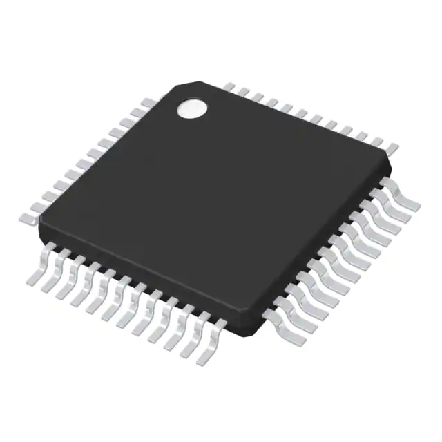


 工商网监
湘ICP备2023018690号
工商网监
湘ICP备2023018690号
