STM32F423xH
Arm®-Cortex®-M4 32b MCU+FPU, 125 DMIPS, 1.5MB Flash,
320KB RAM, USB OTG FS, 1 ADC, 2 DACs, 2 DFSDMs, AES
Datasheet - production data
Features
)%*$
• Dynamic Efficiency Line with eBAM (enhanced
Batch Acquisition Mode)
– 1.7 V to 3.6 V power supply
– -40 °C to 85/105/125 °C temperature range
• Core: Arm® 32-bit Cortex®-M4 CPU with FPU,
Adaptive real-time accelerator (ART
Accelerator™) allowing 0-wait state execution
from Flash memory, frequency up to 100 MHz,
memory protection unit, 125 DMIPS/
1.25 DMIPS/MHz (Dhrystone 2.1), and DSP
instructions
• Memories
– 1.5 Mbytes of Flash memory
– 320 Kbytes of SRAM
– Flexible external static memory controller
with up to 16-bit data bus: SRAM, PSRAM,
NOR Flash memory
– Dual mode Quad-SPI interface
• LCD parallel interface, 8080/6800 modes
• Clock, reset and supply management
– 1.7 to 3.6 V application supply and I/Os
– POR, PDR, PVD and BOR
– 4-to-26 MHz crystal oscillator
– Internal 16 MHz factory-trimmed RC
– 32 kHz oscillator for RTC with calibration
– Internal 32 kHz RC with calibration
• Power consumption
– Run: 112 µA/MHz (peripheral off)
– Stop (Flash in Stop mode, fast wakeup
time): 42 µA Typ.; 80 µA max @25 °C
– Stop (Flash in Deep power down mode,
slow wakeup time): 15 µA Typ.;
46 µA max @25 °C
– Standby without RTC: 1.1 µA Typ.;
14.7 µA max at @85 °C
– VBAT supply for RTC: 1 µA @25 °C
• 2x12-bit D/A converters
• 1×12-bit, 2.4 MSPS ADC: up to 16 channels
• 6x digital filters for sigma delta modulator,
12x PDM interfaces, with stereo microphone
and sound source localization support
• General-purpose DMA: 16-stream DMA
September 2017
This is information on a product in full production.
LQFP64 (10x10mm)
WLCSP81
UFQFPN48
(4.039x3.951 mm) LQFP100 (14x14mm) (7x7 mm)
LQFP144 (20x20mm)
UFBGA100
(7x7mm)
UFBGA144
(10x10mm)
• Up to 18 timers: up to twelve 16-bit timers, two
32-bit timers up to 100 MHz each with up to
four IC/OC/PWM or pulse counter and
quadrature (incremental) encoder input, two
watchdog timers (independent and window),
one SysTick timer, and a low-power timer
• Debug mode
– Serial wire debug (SWD) & JTAG
– Cortex®-M4 Embedded Trace Macrocell™
• Up to 114 I/O ports with interrupt capability
– Up to 109 fast I/Os up to 100 MHz
– Up to 114 five V-tolerant I/Os
• Up to 24 communication interfaces
– Up to 4x I2C interfaces (SMBus/PMBus)
– Up to 10 UARTS: 4 USARTs / 6 UARTs
(2 x 12.5 Mbit/s, 2 x 6.25 Mbit/s), ISO 7816
interface, LIN, IrDA, modem control)
– Up to 5 SPI/I2Ss (up to 50 Mbit/s, SPI or
I2S audio protocol), out of which 2 muxed
full-duplex I2S interfaces
– SDIO interface (SD/MMC/eMMC)
– Advanced connectivity: USB 2.0 full-speed
device/host/OTG controller with PHY
– 3x CAN (2.0B Active)
– 1xSAI
• True random number generator
• CRC calculation unit
• 96-bit unique ID
• RTC: subsecond accuracy, hardware calendar
• 128/256-bit hardware encryption accelerator
(AES)
• All packages are ECOPACK®2
Table 1. Device summary
Reference
STM32F423xH
DocID029161 Rev 7
Part number
STM32F423CH STM32F423MH STM32F423RH
STM32F423VH STM32F423ZH
1/209
www.st.com
�Contents
STM32F423xH
Contents
1
Introduction . . . . . . . . . . . . . . . . . . . . . . . . . . . . . . . . . . . . . . . . . . . . . . . 12
2
Description . . . . . . . . . . . . . . . . . . . . . . . . . . . . . . . . . . . . . . . . . . . . . . . . 13
2.1
3
Functional overview . . . . . . . . . . . . . . . . . . . . . . . . . . . . . . . . . . . . . . . . 19
3.1
Arm® Cortex®-M4 with FPU core with embedded Flash and SRAM . . . . 19
3.2
Adaptive real-time memory accelerator (ART Accelerator™) . . . . . . . . . 19
3.3
Enhanced Batch Acquisition mode (eBAM) . . . . . . . . . . . . . . . . . . . . . . . 19
3.4
Memory protection unit . . . . . . . . . . . . . . . . . . . . . . . . . . . . . . . . . . . . . . . 20
3.5
Embedded Flash memory . . . . . . . . . . . . . . . . . . . . . . . . . . . . . . . . . . . . 20
3.6
CRC (cyclic redundancy check) calculation unit . . . . . . . . . . . . . . . . . . . 20
3.7
Embedded SRAM . . . . . . . . . . . . . . . . . . . . . . . . . . . . . . . . . . . . . . . . . . . 21
3.8
Multi-AHB bus matrix . . . . . . . . . . . . . . . . . . . . . . . . . . . . . . . . . . . . . . . . 21
3.9
DMA controller (DMA) . . . . . . . . . . . . . . . . . . . . . . . . . . . . . . . . . . . . . . . 22
3.10
Flexible static memory controller (FSMC) . . . . . . . . . . . . . . . . . . . . . . . . 22
3.11
Quad-SPI memory interface (QUAD-SPI) . . . . . . . . . . . . . . . . . . . . . . . . 23
3.12
Nested vectored interrupt controller (NVIC) . . . . . . . . . . . . . . . . . . . . . . . 23
3.13
External interrupt/event controller (EXTI) . . . . . . . . . . . . . . . . . . . . . . . . . 23
3.14
Clocks and startup . . . . . . . . . . . . . . . . . . . . . . . . . . . . . . . . . . . . . . . . . . 23
3.15
Boot modes . . . . . . . . . . . . . . . . . . . . . . . . . . . . . . . . . . . . . . . . . . . . . . . 24
3.16
Power supply schemes . . . . . . . . . . . . . . . . . . . . . . . . . . . . . . . . . . . . . . 25
3.17
Power supply supervisor . . . . . . . . . . . . . . . . . . . . . . . . . . . . . . . . . . . . . 26
3.18
2/209
Compatibility with STM32F4 series . . . . . . . . . . . . . . . . . . . . . . . . . . . . . 16
3.17.1
Internal reset ON . . . . . . . . . . . . . . . . . . . . . . . . . . . . . . . . . . . . . . . . . . 26
3.17.2
Internal reset OFF . . . . . . . . . . . . . . . . . . . . . . . . . . . . . . . . . . . . . . . . . 27
Voltage regulator . . . . . . . . . . . . . . . . . . . . . . . . . . . . . . . . . . . . . . . . . . . 27
3.18.1
Regulator ON . . . . . . . . . . . . . . . . . . . . . . . . . . . . . . . . . . . . . . . . . . . . . 28
3.18.2
Regulator OFF . . . . . . . . . . . . . . . . . . . . . . . . . . . . . . . . . . . . . . . . . . . . 28
3.18.3
Regulator ON/OFF and internal reset ON/OFF availability . . . . . . . . . . 31
3.19
Real-time clock (RTC) and backup registers . . . . . . . . . . . . . . . . . . . . . . 31
3.20
Low-power modes . . . . . . . . . . . . . . . . . . . . . . . . . . . . . . . . . . . . . . . . . . 32
3.21
VBAT operation . . . . . . . . . . . . . . . . . . . . . . . . . . . . . . . . . . . . . . . . . . . . 32
DocID029161 Rev 7
�STM32F423xH
3.22
4
Contents
Timers and watchdogs . . . . . . . . . . . . . . . . . . . . . . . . . . . . . . . . . . . . . . . 33
3.22.1
Advanced-control timers (TIM1, TIM8) . . . . . . . . . . . . . . . . . . . . . . . . . 34
3.22.2
General-purpose timers (TIMx) . . . . . . . . . . . . . . . . . . . . . . . . . . . . . . . 34
3.22.3
Basic timer (TIM6, TIM7) . . . . . . . . . . . . . . . . . . . . . . . . . . . . . . . . . . . . 35
3.22.4
Low-power timer (LPTIM1) . . . . . . . . . . . . . . . . . . . . . . . . . . . . . . . . . . 35
3.22.5
Independent watchdog . . . . . . . . . . . . . . . . . . . . . . . . . . . . . . . . . . . . . 35
3.22.6
Window watchdog . . . . . . . . . . . . . . . . . . . . . . . . . . . . . . . . . . . . . . . . . 36
3.22.7
SysTick timer . . . . . . . . . . . . . . . . . . . . . . . . . . . . . . . . . . . . . . . . . . . . . 36
3.23
Inter-integrated circuit interface (I2C) . . . . . . . . . . . . . . . . . . . . . . . . . . . . 36
3.24
Universal synchronous/asynchronous receiver transmitters (USART) . . 36
3.25
Serial peripheral interface (SPI) . . . . . . . . . . . . . . . . . . . . . . . . . . . . . . . . 38
3.26
Inter-integrated sound (I2S) . . . . . . . . . . . . . . . . . . . . . . . . . . . . . . . . . . . 38
3.27
Serial Audio interface (SAI1) . . . . . . . . . . . . . . . . . . . . . . . . . . . . . . . . . . 38
3.28
Audio PLL (PLLI2S) . . . . . . . . . . . . . . . . . . . . . . . . . . . . . . . . . . . . . . . . . 38
3.29
Digital filter for sigma-delta modulators (DFSDM) . . . . . . . . . . . . . . . . . . 39
3.30
Dynamic tuning of PDM delays for sound source localization . . . . . . . . . 39
3.31
Secure digital input/output interface (SDIO) . . . . . . . . . . . . . . . . . . . . . . . 40
3.32
Controller area network (bxCAN) . . . . . . . . . . . . . . . . . . . . . . . . . . . . . . . 40
3.33
Universal serial bus on-the-go full-speed (USB_OTG_FS) . . . . . . . . . . . 40
3.34
Random number generator (RNG) . . . . . . . . . . . . . . . . . . . . . . . . . . . . . . 41
3.35
Advanced encryption standard hardware accelerator (AES) . . . . . . . . . . 41
3.36
General-purpose input/outputs (GPIOs) . . . . . . . . . . . . . . . . . . . . . . . . . . 42
3.37
Analog-to-digital converter (ADC) . . . . . . . . . . . . . . . . . . . . . . . . . . . . . . 42
3.38
Digital to analog converter (DAC) . . . . . . . . . . . . . . . . . . . . . . . . . . . . . . . 42
3.39
Temperature sensor . . . . . . . . . . . . . . . . . . . . . . . . . . . . . . . . . . . . . . . . . 43
3.40
Serial wire JTAG debug port (SWJ-DP) . . . . . . . . . . . . . . . . . . . . . . . . . . 43
3.41
Embedded Trace Macrocell™ . . . . . . . . . . . . . . . . . . . . . . . . . . . . . . . . . 43
Pinouts and pin description . . . . . . . . . . . . . . . . . . . . . . . . . . . . . . . . . . 44
4.1
WLCSP81 pinout description . . . . . . . . . . . . . . . . . . . . . . . . . . . . . . . . . . 44
4.2
UFQFPN48 pinout description . . . . . . . . . . . . . . . . . . . . . . . . . . . . . . . . . 45
4.3
LQFP64 pinout description . . . . . . . . . . . . . . . . . . . . . . . . . . . . . . . . . . . . 46
4.4
LQFP100 pinout description . . . . . . . . . . . . . . . . . . . . . . . . . . . . . . . . . . . 47
4.5
LQFP144 pinout description . . . . . . . . . . . . . . . . . . . . . . . . . . . . . . . . . . . 48
DocID029161 Rev 7
3/209
5
�Contents
STM32F423xH
4.6
UFBGA100 pinout description . . . . . . . . . . . . . . . . . . . . . . . . . . . . . . . . . 49
4.7
UFBGA144 pinout description . . . . . . . . . . . . . . . . . . . . . . . . . . . . . . . . . 50
4.8
Pins definition . . . . . . . . . . . . . . . . . . . . . . . . . . . . . . . . . . . . . . . . . . . . . . 50
4.9
Alternate functions . . . . . . . . . . . . . . . . . . . . . . . . . . . . . . . . . . . . . . . . . . 68
5
Memory mapping . . . . . . . . . . . . . . . . . . . . . . . . . . . . . . . . . . . . . . . . . . . 75
6
Electrical characteristics . . . . . . . . . . . . . . . . . . . . . . . . . . . . . . . . . . . . 79
6.1
4/209
Parameter conditions . . . . . . . . . . . . . . . . . . . . . . . . . . . . . . . . . . . . . . . . 79
6.1.1
Minimum and maximum values . . . . . . . . . . . . . . . . . . . . . . . . . . . . . . . 79
6.1.2
Typical values . . . . . . . . . . . . . . . . . . . . . . . . . . . . . . . . . . . . . . . . . . . . 79
6.1.3
Typical curves . . . . . . . . . . . . . . . . . . . . . . . . . . . . . . . . . . . . . . . . . . . . 79
6.1.4
Loading capacitor . . . . . . . . . . . . . . . . . . . . . . . . . . . . . . . . . . . . . . . . . 79
6.1.5
Pin input voltage . . . . . . . . . . . . . . . . . . . . . . . . . . . . . . . . . . . . . . . . . . 79
6.1.6
Power supply scheme . . . . . . . . . . . . . . . . . . . . . . . . . . . . . . . . . . . . . . 80
6.1.7
Current consumption measurement . . . . . . . . . . . . . . . . . . . . . . . . . . . 81
6.2
Absolute maximum ratings . . . . . . . . . . . . . . . . . . . . . . . . . . . . . . . . . . . . 81
6.3
Operating conditions . . . . . . . . . . . . . . . . . . . . . . . . . . . . . . . . . . . . . . . . 83
6.3.1
General operating conditions . . . . . . . . . . . . . . . . . . . . . . . . . . . . . . . . . 83
6.3.2
VCAP_1/VCAP_2 external capacitors . . . . . . . . . . . . . . . . . . . . . . . . . . 86
6.3.3
Operating conditions at power-up/power-down (regulator ON) . . . . . . . 86
6.3.4
Operating conditions at power-up / power-down (regulator OFF) . . . . . 87
6.3.5
Embedded reset and power control block characteristics . . . . . . . . . . . 87
6.3.6
Supply current characteristics . . . . . . . . . . . . . . . . . . . . . . . . . . . . . . . . 88
6.3.7
Wakeup time from low-power modes . . . . . . . . . . . . . . . . . . . . . . . . . . 106
6.3.8
External clock source characteristics . . . . . . . . . . . . . . . . . . . . . . . . . . 108
6.3.9
Internal clock source characteristics . . . . . . . . . . . . . . . . . . . . . . . . . . 113
6.3.10
PLL characteristics . . . . . . . . . . . . . . . . . . . . . . . . . . . . . . . . . . . . . . . 115
6.3.11
PLL spread spectrum clock generation (SSCG) characteristics . . . . . 117
6.3.12
Memory characteristics . . . . . . . . . . . . . . . . . . . . . . . . . . . . . . . . . . . . 118
6.3.13
EMC characteristics . . . . . . . . . . . . . . . . . . . . . . . . . . . . . . . . . . . . . . . 121
6.3.14
Absolute maximum ratings (electrical sensitivity) . . . . . . . . . . . . . . . . 122
6.3.15
I/O current injection characteristics . . . . . . . . . . . . . . . . . . . . . . . . . . . 123
6.3.16
I/O port characteristics . . . . . . . . . . . . . . . . . . . . . . . . . . . . . . . . . . . . . 124
6.3.17
NRST pin characteristics . . . . . . . . . . . . . . . . . . . . . . . . . . . . . . . . . . . 129
6.3.18
TIM timer characteristics . . . . . . . . . . . . . . . . . . . . . . . . . . . . . . . . . . . 130
DocID029161 Rev 7
�STM32F423xH
7
Contents
6.3.19
Communications interfaces . . . . . . . . . . . . . . . . . . . . . . . . . . . . . . . . . 131
6.3.20
12-bit ADC characteristics . . . . . . . . . . . . . . . . . . . . . . . . . . . . . . . . . . 145
6.3.21
Temperature sensor characteristics . . . . . . . . . . . . . . . . . . . . . . . . . . . 151
6.3.22
VBAT monitoring characteristics . . . . . . . . . . . . . . . . . . . . . . . . . . . . . . 152
6.3.23
Embedded reference voltage . . . . . . . . . . . . . . . . . . . . . . . . . . . . . . . . 152
6.3.24
DAC electrical characteristics . . . . . . . . . . . . . . . . . . . . . . . . . . . . . . . 153
6.3.25
DFSDM characteristics . . . . . . . . . . . . . . . . . . . . . . . . . . . . . . . . . . . . 156
6.3.26
FSMC characteristics . . . . . . . . . . . . . . . . . . . . . . . . . . . . . . . . . . . . . . 159
6.3.27
SD/SDIO MMC/eMMC card host interface (SDIO) characteristics . . . 173
6.3.28
RTC characteristics . . . . . . . . . . . . . . . . . . . . . . . . . . . . . . . . . . . . . . . 175
Package information . . . . . . . . . . . . . . . . . . . . . . . . . . . . . . . . . . . . . . . 176
7.1
WLCSP81 package information . . . . . . . . . . . . . . . . . . . . . . . . . . . . . . . 176
7.2
UFQFPN48 package information . . . . . . . . . . . . . . . . . . . . . . . . . . . . . . 180
7.3
LQFP64 package information . . . . . . . . . . . . . . . . . . . . . . . . . . . . . . . . . 183
7.4
LQFP100 package information . . . . . . . . . . . . . . . . . . . . . . . . . . . . . . . . 187
7.5
LQFP144 package information . . . . . . . . . . . . . . . . . . . . . . . . . . . . . . . . 190
7.6
UFBGA100 package information . . . . . . . . . . . . . . . . . . . . . . . . . . . . . . 194
7.7
UFBGA144 package information . . . . . . . . . . . . . . . . . . . . . . . . . . . . . . 197
7.8
Thermal characteristics . . . . . . . . . . . . . . . . . . . . . . . . . . . . . . . . . . . . . 200
7.8.1
8
Reference document . . . . . . . . . . . . . . . . . . . . . . . . . . . . . . . . . . . . . . 200
Ordering information . . . . . . . . . . . . . . . . . . . . . . . . . . . . . . . . . . . . . . 201
Appendix A Recommendations when using the internal reset OFF . . . . . . . . 202
Appendix B Application block diagrams . . . . . . . . . . . . . . . . . . . . . . . . . . . . . . 203
B.1
Sensor Hub application example. . . . . . . . . . . . . . . . . . . . . . . . . . . . . . . 203
B.2
Display application example . . . . . . . . . . . . . . . . . . . . . . . . . . . . . . . . . . 204
B.3
USB OTG full speed (FS) interface solutions . . . . . . . . . . . . . . . . . . . . . 205
Revision history . . . . . . . . . . . . . . . . . . . . . . . . . . . . . . . . . . . . . . . . . . . . . . . . . . . 207
DocID029161 Rev 7
5/209
5
�List of tables
STM32F423xH
List of tables
Table 1.
Table 2.
Table 3.
Table 4.
Table 5.
Table 6.
Table 7.
Table 8.
Table 9.
Table 10.
Table 11.
Table 12.
Table 13.
Table 14.
Table 15.
Table 16.
Table 17.
Table 18.
Table 19.
Table 20.
Table 21.
Table 22.
Table 23.
Table 24.
Table 25.
Table 26.
Table 27.
Table 28.
Table 29.
Table 30.
Table 31.
Table 32.
Table 33.
Table 34.
Table 35.
Table 36.
Table 37.
Table 38.
Table 39.
Table 40.
6/209
Device summary . . . . . . . . . . . . . . . . . . . . . . . . . . . . . . . . . . . . . . . . . . . . . . . . . . . . . . . . . . 1
STM32F423xH features and peripheral counts . . . . . . . . . . . . . . . . . . . . . . . . . . . . . . . . . 15
Embedded bootloader interfaces . . . . . . . . . . . . . . . . . . . . . . . . . . . . . . . . . . . . . . . . . . . . 24
Regulator ON/OFF and internal power supply supervisor availability. . . . . . . . . . . . . . . . . 31
Timer feature comparison . . . . . . . . . . . . . . . . . . . . . . . . . . . . . . . . . . . . . . . . . . . . . . . . . . 33
Comparison of I2C analog and digital filters . . . . . . . . . . . . . . . . . . . . . . . . . . . . . . . . . . . . 36
USART feature comparison . . . . . . . . . . . . . . . . . . . . . . . . . . . . . . . . . . . . . . . . . . . . . . . . 37
DFSDM feature comparison . . . . . . . . . . . . . . . . . . . . . . . . . . . . . . . . . . . . . . . . . . . . . . . . 39
Legend/abbreviations used in the pinout table . . . . . . . . . . . . . . . . . . . . . . . . . . . . . . . . . . 50
STM32F423xH pin definition . . . . . . . . . . . . . . . . . . . . . . . . . . . . . . . . . . . . . . . . . . . . . . . 51
FSMC pin definition . . . . . . . . . . . . . . . . . . . . . . . . . . . . . . . . . . . . . . . . . . . . . . . . . . . . . . 65
STM32F423xH alternate functions . . . . . . . . . . . . . . . . . . . . . . . . . . . . . . . . . . . . . . . . . . . 68
STM32F423xH register boundary addresses . . . . . . . . . . . . . . . . . . . . . . . . . . . . . . . . . . . 76
Voltage characteristics . . . . . . . . . . . . . . . . . . . . . . . . . . . . . . . . . . . . . . . . . . . . . . . . . . . . 81
Current characteristics . . . . . . . . . . . . . . . . . . . . . . . . . . . . . . . . . . . . . . . . . . . . . . . . . . . . 82
Thermal characteristics. . . . . . . . . . . . . . . . . . . . . . . . . . . . . . . . . . . . . . . . . . . . . . . . . . . . 82
General operating conditions . . . . . . . . . . . . . . . . . . . . . . . . . . . . . . . . . . . . . . . . . . . . . . . 83
Features depending on the operating power supply range . . . . . . . . . . . . . . . . . . . . . . . . 85
VCAP_1/VCAP_2 operating conditions . . . . . . . . . . . . . . . . . . . . . . . . . . . . . . . . . . . . . . . 86
Operating conditions at power-up / power-down (regulator ON) . . . . . . . . . . . . . . . . . . . . 86
Operating conditions at power-up / power-down (regulator OFF). . . . . . . . . . . . . . . . . . . . 87
Embedded reset and power control block characteristics. . . . . . . . . . . . . . . . . . . . . . . . . . 87
Typical and maximum current consumption, code with data processing (ART
accelerator disabled) running from SRAM - VDD = 1.7 V . . . . . . . . . . . . . . . . . . . . . . . . . . 89
Typical and maximum current consumption, code with data processing (ART
accelerator disabled) running from SRAM - VDD = 3.6 V . . . . . . . . . . . . . . . . . . . . . . . . . . 90
Typical and maximum current consumption in run mode, code with data processing
(ART accelerator enabled except prefetch) running from Flash memory- VDD = 1.7 V . . . 91
Typical and maximum current consumption in run mode, code with data processing
(ART accelerator enabled except prefetch) running from Flash memory - VDD = 3.6 V . . 92
Typical and maximum current consumption in run mode, code with data processing
(ART accelerator disabled) running from Flash memory - VDD = 3.6 V. . . . . . . . . . . . . . . 93
Typical and maximum current consumption in run mode, code with data processing
(ART accelerator disabled) running from Flash memory - VDD = 1.7 V. . . . . . . . . . . . . . . 94
Typical and maximum current consumption in run mode, code with data processing
(ART accelerator enabled with prefetch) running from Flash memory - VDD = 3.6 V . . . . . 95
Typical and maximum current consumption in run mode, code with data processing
(ART accelerator enabled with prefetch) running from Flash memory - VDD = 1.7 V . . . . . 96
Typical and maximum current consumption in Sleep mode - VDD = 3.6 V . . . . . . . . . . . . . 97
Typical and maximum current consumption in Sleep mode - VDD = 1.7 V . . . . . . . . . . . . . 98
Typical and maximum current consumptions in Stop mode - VDD = 1.7 V . . . . . . . . . . . . . 99
Typical and maximum current consumption in Stop mode - VDD=3.6 V. . . . . . . . . . . . . . . 99
Typical and maximum current consumption in Standby mode - VDD= 1.7 V . . . . . . . . . . . 99
Typical and maximum current consumption in Standby mode - VDD= 3.6 V . . . . . . . . . . 100
Typical and maximum current consumptions in VBAT mode. . . . . . . . . . . . . . . . . . . . . . . 100
Switching output I/O current consumption . . . . . . . . . . . . . . . . . . . . . . . . . . . . . . . . . . . . 103
Peripheral current consumption . . . . . . . . . . . . . . . . . . . . . . . . . . . . . . . . . . . . . . . . . . . . 104
Low-power mode wakeup timings . . . . . . . . . . . . . . . . . . . . . . . . . . . . . . . . . . . . . . . . . . 108
DocID029161 Rev 7
�STM32F423xH
Table 41.
Table 42.
Table 43.
Table 44.
Table 45.
Table 46.
Table 47.
Table 48.
Table 49.
Table 50.
Table 51.
Table 52.
Table 53.
Table 54.
Table 55.
Table 56.
Table 57.
Table 58.
Table 59.
Table 60.
Table 61.
Table 62.
Table 63.
Table 64.
Table 65.
Table 66.
Table 67.
Table 68.
Table 69.
Table 70.
Table 71.
Table 72.
Table 73.
Table 74.
Table 75.
Table 76.
Table 77.
Table 78.
Table 79.
Table 80.
Table 81.
Table 82.
Table 83.
Table 84.
Table 85.
Table 86.
Table 87.
Table 88.
Table 89.
Table 90.
List of tables
High-speed external user clock characteristics. . . . . . . . . . . . . . . . . . . . . . . . . . . . . . . . . 109
Low-speed external user clock characteristics . . . . . . . . . . . . . . . . . . . . . . . . . . . . . . . . . 109
HSE 4-26 MHz oscillator characteristics. . . . . . . . . . . . . . . . . . . . . . . . . . . . . . . . . . . . . . 111
LSE oscillator characteristics (fLSE = 32.768 kHz) . . . . . . . . . . . . . . . . . . . . . . . . . . . . . . 112
HSI oscillator characteristics . . . . . . . . . . . . . . . . . . . . . . . . . . . . . . . . . . . . . . . . . . . . . . 113
LSI oscillator characteristics . . . . . . . . . . . . . . . . . . . . . . . . . . . . . . . . . . . . . . . . . . . . . . 114
Main PLL characteristics. . . . . . . . . . . . . . . . . . . . . . . . . . . . . . . . . . . . . . . . . . . . . . . . . . 115
PLLI2S (audio PLL) characteristics . . . . . . . . . . . . . . . . . . . . . . . . . . . . . . . . . . . . . . . . . 116
SSCG parameter constraints . . . . . . . . . . . . . . . . . . . . . . . . . . . . . . . . . . . . . . . . . . . . . . 117
Flash memory characteristics . . . . . . . . . . . . . . . . . . . . . . . . . . . . . . . . . . . . . . . . . . . . . . 118
Flash memory programming . . . . . . . . . . . . . . . . . . . . . . . . . . . . . . . . . . . . . . . . . . . . . . . 119
Flash memory programming with VPP voltage . . . . . . . . . . . . . . . . . . . . . . . . . . . . . . . . . 120
Flash memory endurance and data retention . . . . . . . . . . . . . . . . . . . . . . . . . . . . . . . . . . 120
EMS characteristics for LQFP144 package . . . . . . . . . . . . . . . . . . . . . . . . . . . . . . . . . . . 121
EMI characteristics for LQFP144 . . . . . . . . . . . . . . . . . . . . . . . . . . . . . . . . . . . . . . . . . . . 122
ESD absolute maximum ratings . . . . . . . . . . . . . . . . . . . . . . . . . . . . . . . . . . . . . . . . . . . . 123
Electrical sensitivities . . . . . . . . . . . . . . . . . . . . . . . . . . . . . . . . . . . . . . . . . . . . . . . . . . . . 123
I/O current injection susceptibility . . . . . . . . . . . . . . . . . . . . . . . . . . . . . . . . . . . . . . . . . . . 124
I/O static characteristics . . . . . . . . . . . . . . . . . . . . . . . . . . . . . . . . . . . . . . . . . . . . . . . . . . 124
Output voltage characteristics . . . . . . . . . . . . . . . . . . . . . . . . . . . . . . . . . . . . . . . . . . . . . 127
I/O AC characteristics . . . . . . . . . . . . . . . . . . . . . . . . . . . . . . . . . . . . . . . . . . . . . . . . . . . . 128
NRST pin characteristics . . . . . . . . . . . . . . . . . . . . . . . . . . . . . . . . . . . . . . . . . . . . . . . . . 129
TIMx characteristics . . . . . . . . . . . . . . . . . . . . . . . . . . . . . . . . . . . . . . . . . . . . . . . . . . . . . 130
I2C characteristics. . . . . . . . . . . . . . . . . . . . . . . . . . . . . . . . . . . . . . . . . . . . . . . . . . . . . . . 131
SCL frequency (fPCLK1= 50 MHz, VDD = VDD_I2C = 3.3 V) . . . . . . . . . . . . . . . . . . . . . . . . 132
FMPI2C characteristics . . . . . . . . . . . . . . . . . . . . . . . . . . . . . . . . . . . . . . . . . . . . . . . . . . . 133
SPI dynamic characteristics . . . . . . . . . . . . . . . . . . . . . . . . . . . . . . . . . . . . . . . . . . . . . . . 135
I2S dynamic characteristics . . . . . . . . . . . . . . . . . . . . . . . . . . . . . . . . . . . . . . . . . . . . . . . 138
SAI characteristics . . . . . . . . . . . . . . . . . . . . . . . . . . . . . . . . . . . . . . . . . . . . . . . . . . . . . . 140
QSPI dynamic characteristics in SDR mode. . . . . . . . . . . . . . . . . . . . . . . . . . . . . . . . . . . 142
QSPI dynamic characteristics in DDR mode . . . . . . . . . . . . . . . . . . . . . . . . . . . . . . . . . . 142
USB OTG FS startup time . . . . . . . . . . . . . . . . . . . . . . . . . . . . . . . . . . . . . . . . . . . . . . . . 143
USB OTG FS DC electrical characteristics. . . . . . . . . . . . . . . . . . . . . . . . . . . . . . . . . . . . 143
USB OTG FS electrical characteristics . . . . . . . . . . . . . . . . . . . . . . . . . . . . . . . . . . . . . . . 144
ADC characteristics . . . . . . . . . . . . . . . . . . . . . . . . . . . . . . . . . . . . . . . . . . . . . . . . . . . . . 145
ADC accuracy at fADC = 18 MHz . . . . . . . . . . . . . . . . . . . . . . . . . . . . . . . . . . . . . . . . . . . 146
ADC accuracy at fADC = 30 MHz . . . . . . . . . . . . . . . . . . . . . . . . . . . . . . . . . . . . . . . . . . . 147
ADC accuracy at fADC = 36 MHz . . . . . . . . . . . . . . . . . . . . . . . . . . . . . . . . . . . . . . . . . . . 147
ADC dynamic accuracy at fADC = 18 MHz - limited test conditions . . . . . . . . . . . . . . . . . 147
ADC dynamic accuracy at fADC = 36 MHz - limited test conditions . . . . . . . . . . . . . . . . . 147
Temperature sensor characteristics . . . . . . . . . . . . . . . . . . . . . . . . . . . . . . . . . . . . . . . . . 151
Temperature sensor calibration values. . . . . . . . . . . . . . . . . . . . . . . . . . . . . . . . . . . . . . . 151
VBAT monitoring characteristics . . . . . . . . . . . . . . . . . . . . . . . . . . . . . . . . . . . . . . . . . . . . 152
Embedded internal reference voltage . . . . . . . . . . . . . . . . . . . . . . . . . . . . . . . . . . . . . . . . 152
Internal reference voltage calibration values . . . . . . . . . . . . . . . . . . . . . . . . . . . . . . . . . . 152
DAC characteristics . . . . . . . . . . . . . . . . . . . . . . . . . . . . . . . . . . . . . . . . . . . . . . . . . . . . . 153
DFSDM characteristics . . . . . . . . . . . . . . . . . . . . . . . . . . . . . . . . . . . . . . . . . . . . . . . . . . . 156
Asynchronous non-multiplexed SRAM/PSRAM/NOR read timings . . . . . . . . . . . . . . . . . . . . . . . . . . . . . . . . . . . . . . . . . . . . . . . . . . . . . . . . . . . 161
Asynchronous non-multiplexed SRAM/PSRAM/NOR read NWAIT timings . . . . . . . . . . . . . . . . . . . . . . . . . . . . . . . . . . . . . . . . . . . . . . . . . . . . . . . . . 161
Asynchronous non-multiplexed SRAM/PSRAM/NOR write timings . . . . . . . . . . . . . . . . . 162
DocID029161 Rev 7
7/209
8
�List of tables
Table 91.
Table 92.
Table 93.
Table 94.
Table 95.
Table 96.
Table 97.
Table 98.
Table 99.
Table 100.
Table 101.
Table 102.
Table 103.
Table 104.
Table 105.
Table 106.
Table 107.
Table 108.
Table 109.
Table 110.
Table 111.
Table 112.
Table 113.
Table 114.
Table 115.
8/209
STM32F423xH
Asynchronous non-multiplexed SRAM/PSRAM/NOR write NWAIT timings . . . . . . . . . . . . . . . . . . . . . . . . . . . . . . . . . . . . . . . . . . . . . . . . . . . . . . . . . 163
Asynchronous multiplexed PSRAM/NOR read timings. . . . . . . . . . . . . . . . . . . . . . . . . . . 164
Asynchronous multiplexed PSRAM/NOR read-NWAIT timings . . . . . . . . . . . . . . . . . . . . 164
Asynchronous multiplexed PSRAM/NOR write timings . . . . . . . . . . . . . . . . . . . . . . . . . . 166
Asynchronous multiplexed PSRAM/NOR write-NWAIT timings . . . . . . . . . . . . . . . . . . . . 166
Synchronous multiplexed NOR/PSRAM read timings . . . . . . . . . . . . . . . . . . . . . . . . . . . 168
Synchronous multiplexed PSRAM write timings . . . . . . . . . . . . . . . . . . . . . . . . . . . . . . . . 170
Synchronous non-multiplexed NOR/PSRAM read timings . . . . . . . . . . . . . . . . . . . . . . . . 171
Synchronous non-multiplexed PSRAM write timings . . . . . . . . . . . . . . . . . . . . . . . . . . . . 172
SD / MMC characteristics . . . . . . . . . . . . . . . . . . . . . . . . . . . . . . . . . . . . . . . . . . . . . . . . . 174
eMMC characteristics VDD = 1.7 V to 1.9 V. . . . . . . . . . . . . . . . . . . . . . . . . . . . . . . . . . . 174
RTC characteristics . . . . . . . . . . . . . . . . . . . . . . . . . . . . . . . . . . . . . . . . . . . . . . . . . . . . . 175
WLCSP81 - 81-ball, 4.039 x 3.951 mm, 0.4 mm pitch wafer level chip scale
package mechanical data . . . . . . . . . . . . . . . . . . . . . . . . . . . . . . . . . . . . . . . . . . . . . . . . . 177
WLCSP81 recommended PCB design rules (0.4 mm pitch) . . . . . . . . . . . . . . . . . . . . . . 178
UFQFPN48 - 48-lead, 7x7 mm, 0.5 mm pitch, ultra thin fine pitch quad flat
package mechanical data . . . . . . . . . . . . . . . . . . . . . . . . . . . . . . . . . . . . . . . . . . . . . . . . . 181
LQFP64 - 64-pin, 10 x 10 mm low-profile quad flat
package mechanical data . . . . . . . . . . . . . . . . . . . . . . . . . . . . . . . . . . . . . . . . . . . . . . . . . 184
LQPF100 - 100-pin, 14 x 14 mm low-profile quad flat package
mechanical data . . . . . . . . . . . . . . . . . . . . . . . . . . . . . . . . . . . . . . . . . . . . . . . . . . . . . . . . 187
LQFP144 - 144-pin, 20 x 20 mm low-profile quad flat package
mechanical data . . . . . . . . . . . . . . . . . . . . . . . . . . . . . . . . . . . . . . . . . . . . . . . . . . . . . . . . 191
UFBGA100 - 100-ball, 7 x 7 mm, 0.50 mm pitch, ultra fine pitch ball
grid array package mechanical data . . . . . . . . . . . . . . . . . . . . . . . . . . . . . . . . . . . . . . . . . 194
UFBGA100 recommended PCB design rules (0.5 mm pitch BGA) . . . . . . . . . . . . . . . . . 195
UFBGA144 - 144-ball, 10 x 10 mm, 0.80 mm pitch, ultra fine pitch ball grid
array package mechanical data . . . . . . . . . . . . . . . . . . . . . . . . . . . . . . . . . . . . . . . . . . . . 197
UFBGA144 recommended PCB design rules (0.80 mm pitch BGA) . . . . . . . . . . . . . . . . 198
Package thermal characteristics . . . . . . . . . . . . . . . . . . . . . . . . . . . . . . . . . . . . . . . . . . . . 200
Ordering information scheme . . . . . . . . . . . . . . . . . . . . . . . . . . . . . . . . . . . . . . . . . . . . . . 201
Document revision history . . . . . . . . . . . . . . . . . . . . . . . . . . . . . . . . . . . . . . . . . . . . . . . . 207
DocID029161 Rev 7
�STM32F423xH
List of figures
List of figures
Figure 1.
Figure 2.
Figure 3.
Figure 4.
Figure 5.
Figure 6.
Figure 7.
Figure 8.
Figure 9.
Figure 10.
Figure 11.
Figure 12.
Figure 13.
Figure 14.
Figure 15.
Figure 16.
Figure 17.
Figure 18.
Figure 19.
Figure 20.
Figure 21.
Figure 22.
Figure 23.
Figure 24.
Figure 25.
Figure 26.
Figure 27.
Figure 28.
Figure 29.
Figure 30.
Figure 31.
Figure 32.
Figure 33.
Figure 34.
Figure 35.
Figure 36.
Figure 37.
Figure 38.
Figure 39.
Figure 40.
Figure 41.
Figure 42.
Figure 43.
Figure 44.
Compatible board design for LQFP100 package . . . . . . . . . . . . . . . . . . . . . . . . . . . . . . . . 16
Compatible board design for LQFP64 package . . . . . . . . . . . . . . . . . . . . . . . . . . . . . . . . . 17
Compatible board design for LQFP144 package . . . . . . . . . . . . . . . . . . . . . . . . . . . . . . . . 17
STM32F423xH block diagram . . . . . . . . . . . . . . . . . . . . . . . . . . . . . . . . . . . . . . . . . . . . . . 18
Multi-AHB matrix . . . . . . . . . . . . . . . . . . . . . . . . . . . . . . . . . . . . . . . . . . . . . . . . . . . . . . . . . 21
VDDUSB connected to an external independent power supply . . . . . . . . . . . . . . . . . . . . . 26
Power supply supervisor interconnection with internal reset OFF . . . . . . . . . . . . . . . . . . . 27
Regulator OFF . . . . . . . . . . . . . . . . . . . . . . . . . . . . . . . . . . . . . . . . . . . . . . . . . . . . . . . . . . 29
Startup in regulator OFF: slow VDD slope
power-down reset risen after VCAP_1/VCAP_2 stabilization . . . . . . . . . . . . . . . . . . . . . . . . . 30
Startup in regulator OFF mode: fast VDD slope
power-down reset risen before VCAP_1/VCAP_2 stabilization. . . . . . . . . . . . . . . . . . . . . . . . 30
STM32F423xH WLCSP81 pinout . . . . . . . . . . . . . . . . . . . . . . . . . . . . . . . . . . . . . . . . . . . . 44
STM32F423xH UFQFPN48 pinout . . . . . . . . . . . . . . . . . . . . . . . . . . . . . . . . . . . . . . . . . . . 45
STM32F423xH LQFP64 pinout . . . . . . . . . . . . . . . . . . . . . . . . . . . . . . . . . . . . . . . . . . . . . 46
STM32F423xH LQFP100 pinout . . . . . . . . . . . . . . . . . . . . . . . . . . . . . . . . . . . . . . . . . . . . 47
STM32F423xH LQFP144 pinout . . . . . . . . . . . . . . . . . . . . . . . . . . . . . . . . . . . . . . . . . . . . 48
STM32F423xH UFBGA100 pinout . . . . . . . . . . . . . . . . . . . . . . . . . . . . . . . . . . . . . . . . . . . 49
STM32F423xH UFBGA144 pinout . . . . . . . . . . . . . . . . . . . . . . . . . . . . . . . . . . . . . . . . . . . 50
Memory map . . . . . . . . . . . . . . . . . . . . . . . . . . . . . . . . . . . . . . . . . . . . . . . . . . . . . . . . . . . . 75
Pin loading conditions . . . . . . . . . . . . . . . . . . . . . . . . . . . . . . . . . . . . . . . . . . . . . . . . . . . . . 79
Input voltage measurement . . . . . . . . . . . . . . . . . . . . . . . . . . . . . . . . . . . . . . . . . . . . . . . . 79
Power supply scheme. . . . . . . . . . . . . . . . . . . . . . . . . . . . . . . . . . . . . . . . . . . . . . . . . . . . . 80
Current consumption measurement scheme . . . . . . . . . . . . . . . . . . . . . . . . . . . . . . . . . . . 81
External capacitor CEXT . . . . . . . . . . . . . . . . . . . . . . . . . . . . . . . . . . . . . . . . . . . . . . . . . . . 86
Typical VBAT current consumption (LSE and RTC ON/LSE oscillator
“low power” mode selection) . . . . . . . . . . . . . . . . . . . . . . . . . . . . . . . . . . . . . . . . . . . . . . 101
Typical VBAT current consumption (LSE and RTC ON/LSE oscillator
“high drive” mode selection) . . . . . . . . . . . . . . . . . . . . . . . . . . . . . . . . . . . . . . . . . . . . . . 101
Low-power mode wakeup . . . . . . . . . . . . . . . . . . . . . . . . . . . . . . . . . . . . . . . . . . . . . . . . . 107
High-speed external clock source AC timing diagram . . . . . . . . . . . . . . . . . . . . . . . . . . . 110
Low-speed external clock source AC timing diagram . . . . . . . . . . . . . . . . . . . . . . . . . . . . 110
Typical application with an 8 MHz crystal . . . . . . . . . . . . . . . . . . . . . . . . . . . . . . . . . . . . . 111
Typical application with a 32.768 kHz crystal . . . . . . . . . . . . . . . . . . . . . . . . . . . . . . . . . . 112
ACCHSI versus temperature . . . . . . . . . . . . . . . . . . . . . . . . . . . . . . . . . . . . . . . . . . . . . . . 113
ACCLSI versus temperature . . . . . . . . . . . . . . . . . . . . . . . . . . . . . . . . . . . . . . . . . . . . . . . 114
PLL output clock waveforms in center spread mode . . . . . . . . . . . . . . . . . . . . . . . . . . . . 118
PLL output clock waveforms in down spread mode . . . . . . . . . . . . . . . . . . . . . . . . . . . . . 118
FT/TC I/O input characteristics . . . . . . . . . . . . . . . . . . . . . . . . . . . . . . . . . . . . . . . . . . . . . 126
I/O AC characteristics definition . . . . . . . . . . . . . . . . . . . . . . . . . . . . . . . . . . . . . . . . . . . . 129
Recommended NRST pin protection . . . . . . . . . . . . . . . . . . . . . . . . . . . . . . . . . . . . . . . . 130
I2C bus AC waveforms and measurement circuit . . . . . . . . . . . . . . . . . . . . . . . . . . . . . . . 132
FMPI2C timing diagram and measurement circuit . . . . . . . . . . . . . . . . . . . . . . . . . . . . . . 134
SPI timing diagram - slave mode and CPHA = 0 . . . . . . . . . . . . . . . . . . . . . . . . . . . . . . . 136
SPI timing diagram - slave mode and CPHA = 1 . . . . . . . . . . . . . . . . . . . . . . . . . . . . . . . 137
SPI timing diagram - master mode . . . . . . . . . . . . . . . . . . . . . . . . . . . . . . . . . . . . . . . . . . 137
I2S slave timing diagram (Philips protocol) . . . . . . . . . . . . . . . . . . . . . . . . . . . . . . . . . . . 139
I2S master timing diagram (Philips protocol). . . . . . . . . . . . . . . . . . . . . . . . . . . . . . . . . . . 139
DocID029161 Rev 7
9/209
11
�List of figures
Figure 45.
Figure 46.
Figure 47.
Figure 48.
Figure 49.
Figure 50.
Figure 51.
Figure 52.
Figure 53.
Figure 54.
Figure 55.
Figure 56.
Figure 57.
Figure 58.
Figure 59.
Figure 60.
Figure 61.
Figure 62.
Figure 63.
Figure 64.
Figure 65.
Figure 66.
Figure 67.
Figure 68.
Figure 69.
Figure 70.
Figure 71.
Figure 72.
Figure 73.
Figure 74.
Figure 75.
Figure 76.
Figure 77.
Figure 78.
Figure 79.
Figure 80.
Figure 81.
Figure 82.
Figure 83.
Figure 84.
Figure 85.
Figure 86.
Figure 87.
10/209
STM32F423xH
SAI master timing waveforms . . . . . . . . . . . . . . . . . . . . . . . . . . . . . . . . . . . . . . . . . . . . . . 141
SAI slave timing waveforms . . . . . . . . . . . . . . . . . . . . . . . . . . . . . . . . . . . . . . . . . . . . . . . 141
USB OTG FS timings: definition of data signal rise and fall time . . . . . . . . . . . . . . . . . . . 144
ADC accuracy characteristics . . . . . . . . . . . . . . . . . . . . . . . . . . . . . . . . . . . . . . . . . . . . . . 148
Typical connection diagram using the ADC . . . . . . . . . . . . . . . . . . . . . . . . . . . . . . . . . . . 149
Power supply and reference decoupling (VREF+ not connected to VDDA). . . . . . . . . . . . . 150
Power supply and reference decoupling (VREF+ connected to VDDA). . . . . . . . . . . . . . . . 151
12-bit buffered /non-buffered DAC . . . . . . . . . . . . . . . . . . . . . . . . . . . . . . . . . . . . . . . . . . 155
Asynchronous non-multiplexed SRAM/PSRAM/NOR read waveforms . . . . . . . . . . . . . . 160
Asynchronous non-multiplexed SRAM/PSRAM/NOR write waveforms . . . . . . . . . . . . . . 162
Asynchronous multiplexed PSRAM/NOR read waveforms. . . . . . . . . . . . . . . . . . . . . . . . 163
Asynchronous multiplexed PSRAM/NOR write waveforms . . . . . . . . . . . . . . . . . . . . . . . 165
Synchronous multiplexed NOR/PSRAM read timings . . . . . . . . . . . . . . . . . . . . . . . . . . . 167
Synchronous multiplexed PSRAM write timings . . . . . . . . . . . . . . . . . . . . . . . . . . . . . . . . 169
Synchronous non-multiplexed NOR/PSRAM read timings . . . . . . . . . . . . . . . . . . . . . . . . 171
Synchronous non-multiplexed PSRAM write timings . . . . . . . . . . . . . . . . . . . . . . . . . . . . 172
SDIO high-speed mode . . . . . . . . . . . . . . . . . . . . . . . . . . . . . . . . . . . . . . . . . . . . . . . . . . 173
SD default mode . . . . . . . . . . . . . . . . . . . . . . . . . . . . . . . . . . . . . . . . . . . . . . . . . . . . . . . . 173
WLCSP81 - 81-ball, 4.039 x 3.951 mm, 0.4 mm pitch wafer level chip scale
package outline. . . . . . . . . . . . . . . . . . . . . . . . . . . . . . . . . . . . . . . . . . . . . . . . . . . . . . . . . 176
WLCSP81- 81-ball, 4.039 x 3.951 mm, 0.4 mm pitch wafer level chip scale
package recommended footprint . . . . . . . . . . . . . . . . . . . . . . . . . . . . . . . . . . . . . . . . . . . 178
WLCSP81 marking example (package top view) . . . . . . . . . . . . . . . . . . . . . . . . . . . . . . . 179
UFQFPN48 - 48-lead, 7x7 mm, 0.5 mm pitch, ultra thin fine pitch quad flat
package outline. . . . . . . . . . . . . . . . . . . . . . . . . . . . . . . . . . . . . . . . . . . . . . . . . . . . . . . . . 180
UFQFPN48 recommended footprint . . . . . . . . . . . . . . . . . . . . . . . . . . . . . . . . . . . . . . . . . 181
UFQFPN48 marking example (package top view) . . . . . . . . . . . . . . . . . . . . . . . . . . . . . . 182
LQFP64 - 64-pin, 10 x 10 mm low-profile quad flat package outline . . . . . . . . . . . . . . . . 183
LQFP64 recommended footprint . . . . . . . . . . . . . . . . . . . . . . . . . . . . . . . . . . . . . . . . . . . 185
LQFP64 marking example (package top view) . . . . . . . . . . . . . . . . . . . . . . . . . . . . . . . . 186
LQFP100 - 100-pin, 14 x 14 mm low-profile quad flat package outline . . . . . . . . . . . . . . 187
LQFP100 - 100-pin, 14 x 14 mm low-profile quad flat
recommended footprint . . . . . . . . . . . . . . . . . . . . . . . . . . . . . . . . . . . . . . . . . . . . . . . . . . . 188
LQFP100 marking example (package top view) . . . . . . . . . . . . . . . . . . . . . . . . . . . . . . . 189
LQFP144 - 144-pin, 20 x 20 mm low-profile quad flat package outline . . . . . . . . . . . . . . 190
LQFP144 - 144-pin,20 x 20 mm low-profile quad flat package
recommended footprint . . . . . . . . . . . . . . . . . . . . . . . . . . . . . . . . . . . . . . . . . . . . . . . . . . . 192
LQFP144 marking example (package top view) . . . . . . . . . . . . . . . . . . . . . . . . . . . . . . . 193
UFBGA100 - 100-pin, 7 x 7 mm, 0.50 mm pitch, ultra fine pitch ball
grid array package outline . . . . . . . . . . . . . . . . . . . . . . . . . . . . . . . . . . . . . . . . . . . . . . . . 194
UFBGA100 - 100-pin, 7 x 7 mm, 0.50 mm pitch, ultra fine pitch ball
grid array package recommended footprint . . . . . . . . . . . . . . . . . . . . . . . . . . . . . . . . . . . 195
UFBGA100 marking example (package top view) . . . . . . . . . . . . . . . . . . . . . . . . . . . . . . 196
UFBGA144 - 144-pin, 10 x 10 mm, 0.80 mm pitch, ultra fine pitch ball
grid array package outline . . . . . . . . . . . . . . . . . . . . . . . . . . . . . . . . . . . . . . . . . . . . . . . . 197
UFBGA144 - 144-pin, 10 x 10 mm, 0.80 mm pitch, ultra fine pitch ball
grid array recommended footprint. . . . . . . . . . . . . . . . . . . . . . . . . . . . . . . . . . . . . . . . . . . 198
UFBGA144 marking example (package top view) . . . . . . . . . . . . . . . . . . . . . . . . . . . . . . 199
Sensor Hub application example . . . . . . . . . . . . . . . . . . . . . . . . . . . . . . . . . . . . . . . . . . . 203
Display application example . . . . . . . . . . . . . . . . . . . . . . . . . . . . . . . . . . . . . . . . . . . . . . . 204
USB controller configured as peripheral-only and used in Full speed mode . . . . . . . . . . 205
USB peripheral-only Full speed mode with direct connection
DocID029161 Rev 7
�STM32F423xH
Figure 88.
Figure 89.
List of figures
for VBUS sense . . . . . . . . . . . . . . . . . . . . . . . . . . . . . . . . . . . . . . . . . . . . . . . . . . . . . . . . 205
USB peripheral-only Full speed mode, VBUS detection using GPIO . . . . . . . . . . . . . . . . 206
USB controller configured as host-only and used in full speed mode. . . . . . . . . . . . . . . . 206
DocID029161 Rev 7
11/209
11
�Introduction
1
STM32F423xH
Introduction
This datasheet provides the description of the STM32F423xH microcontrollers.
For information on the Cortex®-M4 core, please refer to the Cortex®-M4 programming
manual (PM0214) available from www.st.com.
12/209
DocID029161 Rev 7
�STM32F423xH
2
Description
Description
The STM32F423XH devices are based on the high-performance Arm® Cortex®-M4 32-bit
RISC core operating at a frequency of up to 100 MHz. Their Cortex®-M4 core features a
Floating point unit (FPU) single precision which supports all Arm single-precision dataprocessing instructions and data types. It also implements a full set of DSP instructions and
a memory protection unit (MPU) which enhances application security.
The STM32F423XH devices belong to the STM32F423xH access product lines (with
products combining power efficiency, performance and integration) while adding a new
innovative feature called Batch Acquisition Mode (BAM) allowing to save even more power
consumption during data batching.
The STM32F423XH devices incorporate high-speed embedded memories (1.5 Mbytes of
Flash memory, 320 Kbytes of SRAM), and an extensive range of enhanced I/Os and
peripherals connected to two APB buses, three AHB buses and a 32-bit multi-AHB bus
matrix.
All devices offer a 12-bit ADC, two 12-bit DACs, a low-power RTC, twelve general-purpose
16-bit timers including two PWM timer for motor control, two general-purpose 32-bit timers
and a low power timer.
They also feature standard and advanced communication interfaces.
•
Up to four I2Cs, including one I2C supporting Fast-Mode Plus
•
Five SPIs
•
Five I2Ss out of which two are full duplex. To achieve audio class accuracy, the I2S
peripherals can be clocked via a dedicate internal audio PLL or via an external clock to
allow synchronization.
•
Four USARTs and six UARTs
•
An SDIO/MMC interface
•
An USB 2.0 OTG full-speed interface
•
Three CANs
•
An SAI.
In addition, the STM32F423xH devices embed advanced peripherals:
•
A flexible static memory control interface (FSMC)
•
A Quad-SPI memory interface
•
Two digital filter for sigma modulator (DFSDM) supporting microphone MEMs and
sound source localization, one with two filters and up to four inputs, and the second
one with four filters and up to eight inputs
The STM32F423xH devices embed an AES hardware accelerator.
They are offered in 7 packages ranging from 48 to 144 pins. The set of available peripherals
depends on the selected package. The STM32F423xH operate in the – 40 to + 125 °C
temperature range from a 1.7 (PDR OFF) to 3.6 V power supply. A comprehensive set of
power-saving mode allows the design of low-power applications.
DocID029161 Rev 7
13/209
43
�Description
STM32F423xH
These features make the STM32F423xH microcontrollers suitable for a wide range of
applications:
14/209
•
Motor drive and application control
•
Medical equipment
•
Industrial applications: PLC, inverters, circuit breakers
•
Printers, and scanners
•
Alarm systems, video intercom, and HVAC
•
Home audio appliances
•
Mobile phone sensor hub
•
Wearable devices
•
Connected objects
•
Wifi modules
DocID029161 Rev 7
�STM32F423xH
Description
Table 2. STM32F423xH features and peripheral counts
Peripherals
STM32F423xH
Flash memory (Kbyte)
SRAM (Kbyte)
1536
System
320 (256 + 64)
FSMC memory controller
-
1(1)
FSMC LCD parallel interface
Data bus size
-
8
Quad-SPI memory interface
-
Timers
General-purpose
10(2)
Advanced-control
2(4)
1(1)
1
10
10
(3)
Low-power timer
1
Random number generator
1
AES
1
Comm. interfaces
I2S
5/5 (2 full duplex)
I2C
3
I2CFMP
1
3/3
4/3
SDIO/MMC
1
No
Dual power rail
1
Yes
CAN
3
SAI
1
Number of digital Filtersfor Sigmadelta modulator
7
11
GPIOs
36
50
1
Yes
12
60
81
114
1
12-bit ADC
10
16
Yes
12-bit DAC
Number of channels
2
Maximum CPU frequency
100 MHz
Operating voltage
Operating temperatures
1
No
6
Number of channels
Package
4/6
1
USB/OTG FS
Number of channels
10
2
2
USART/UART
1
16
Basic
SPI/
1(1)
1.7 to 3.6 V
Ambient temperatures: – 40 to + 85 °C/– 40 to + 105 °C / – 40 to + 125 °C
Junction temperature: – 40 to + 130 °C
UFQFPN48
LQFP64
WLCSP81
UFBGA100
LQFP100
UFBGA144
LQFP144
1. 64 pins packages support only 8 bits multiplexed mode interface
81 pins packages support 1 external memory of up to 64KB in multiplexed mode
100 pins packages support 2 external memories of up to 64MB in multiplexed mode
Refer to Table 11: FSMC pin definition for more detailed information.
2. 48 pins packages: TIM3 and TIM4: ETR pin not available.
DocID029161 Rev 7
15/209
43
�Description
STM32F423xH
3. 81 pins packages: TIM4: ETR pin not available.
4. 48 pins packages: TIM8:CH1, CH2, CH3 and CH4 pins not available.
2.1
Compatibility with STM32F4 series
The STM32F423xH are fully software and feature compatible with the STM32F4 series
(STM32F42x, STM32F401, STM32F43x, STM32F41x, STM32F405 and STM32F407)
The STM32F423xH can be used as drop-in replacement of the other STM32F4 products but
some slight changes have to be done on the PCB board.
Figure 1. Compatible board design for LQFP100 package
670��)���[[
670��)���[[
670��)���[[
670��)���[[
670��)���[[
670��)���[[
670��)���[[
670��)����670��)����OLQH
670��)����670��)����OLQH
670��)����670��)����OLQH
670��)����670��)����OLQH
��
��
��
��
��
��
��
��
��
��
3(��
3(��
3(��
3(��
3(��
3(��
3%��
9&$3B�
966
9''
3%�� QRW DYDLODEOH�DQ\PRUH
5HSODFHG E\ 9 &$3B�
��
��
��
��
��
��
��
��
��
��
��
��
��
��
��
��
��
��
3'������
3'������
3'�
3'�
3%��
3%��
3%��
3%��
3(��
3(��
3(��
3(��
3(��
3(��
3%��
3%��
9&$3B�
9''
��
��
��
��
��
��
��
��
966 9''
3'������
3'������
3'�
3'�
3%��
3%��
3%��
3%��
966 9''
06Y�����9�
16/209
DocID029161 Rev 7
�STM32F423xH
Description
Figure 2. Compatible board design for LQFP64 package
670��)���[[
670��)���[[
670��)���[[
670��)���[[
670��)���[[
670��)���[[
670��)���[[
9''
9&$3B�
3$��
3$��
3$��
3$��
3$�
3$�
3&�
3&�
3&�
3&�
3%��
3%��
3%��
3%��
9''
966
�� ������ ��
��
��
��
��
��
��
��
��
��
��
��
��
3%���QRW�DYDLODEOH�DQ\PRUH��
��
5HSODFHG�E\�9&$3B�
��
��
��
�� ���� ����
9''
966
3$��
3$��
3$��
3$��
3$�
966
3$�
3&�
3&�
3&�
3&�
3%��
3%��
3%��
3%��
9''
3%�
3%��
9&$3B�
966
9''
3%�
3%��
3%��
9&$3B�
9''
�� ������ ��
��
��
��
��
��
��
��
��
��
��
��
��
��
��
��
��
�� ���� ����
3&��
3&��
3&��
3$��
3$��
3&��
3&��
3&��
3$��
3$��
670��)����670��)����OLQH
9&$3B��LQFUHDVHG�WR�����I
(65����RU�EHORZ����
966
9 6 6 9 ''
9''
06Y�����9�
Figure 3. Compatible board design for LQFP144 package
670��)���[
670��)���[
670��)���[
670��)���[[
3'�
3'�
3&��
3&��
3&��
3$��
3$��
���
���
���
���
���
���
���
���
���
���
���
���
���
���
3'�
3'�
3&��
3&��
3&��
3$��
3$��
670��)����670��)����OLQH
670��)����670��)����OLQH
670��)����670��)����OLQH
670��)����670��)����OLQH
���
���
���
���
���
���
���
���
���
��
��
��
��
��
��
��
9''
966
9&$3B�
3$��
3$��
3$��
3$��
3$�
3$�
3&�
3&�
3&�
3&�
9''
966
3*�
6HSDUDWH�86%�SRZHU�UDLO�
&RQQHFWHG�WR�9''�LI�D�GLIIHUHQW�
SRZHU�VXSSO\�IRU�WKH�86%�LV�QRW�
UHTXLUHG�
���
���
���
���
���
���
���
���
���
��
��
��
��
��
��
��
9''
966
9&$3B�
3$��
3$��
3$��
3$��
3$�
3$�
3&�
3&�
3&�
3&�
9''86%
966
3*�
06Y�����9�
DocID029161 Rev 7
17/209
43
�Description
STM32F423xH
Figure 4. STM32F423xH block diagram
038�)38
(70
)60&
125�)ODVK��
65$0��365$0
$+%�
-7$*� �6:
����.%�65$0�
,�%86
���.%�65$0�
6�%86
����0%
)ODVK�PHPRU\
),)2
'�%86
$&&(/�
&$&+(
$50�&RUWH[�0�
&RUWH[�0�
����0+]
&/.��1(>���@��$>����@�
'>����@��12(1��1:(1�
1%/>���@��1:$,7
&/.��&6$��&6%��'>���@
4XDG�63,
19,&
$+%�EXV�PDWUL[��6�0
-7567��-7',�
-7&.�6:&/.
-7'2�6:'��-7'2
75$&(&/.
75$&('>���@
7LQ\�$(6
51*
),)2
*3,2�3257�$
3%>����@
*3,2�3257�%
$+%������0+]
��6WUHDPV
'0$�
3$>����@
),)2
��6WUHDPV
'0$�
9''
),)2
#9''$
325��
UHVHW
*3,2�3257�&
,QW
3//��3//�
3'>����@
*3,2�3257�'
3(>����@
*3,2�3257�(
86%
27*�)6
3RZHU�PDQDJPW
9ROWDJH�
UHJXODWRU
����WR�����9
9''$��966$
1567
39'
#9''
;7$/�26&
�����0+]
*3,2�3257�+
5HVHW�
FORFN
0 $1
$*7
FRQWURO
3:5
LQWHUIDFH
/6
/6
��3:0����3:0�
(75��%.,1�DV�$)
7,0����3:0
��E
��3:0����3:0�
(75��%.,1�DV�$)
7,0����3:0
��E
7,0�
��E
��FKDQQHO�DV�$)
7,0��
��E
��FKDQQHO�DV�$)
7,0��
��E
VPFDUG
5;��7;��6&.�
&76��576�DV�$)
VPFDUG
86$57�
LU'$
LU'$
86$57�
5;��7;�DV�$)�
8$57�
5;��7;�DV�$)�
8$57��
026,��0,62��
6&.���166�:6�DV�$)
63,��,�6�
7,0(5�
��E
��FKDQQHOV�DV�$)
��FKDQQHOV�DV�$)
7,0�
��E
��FKDQQHOV�DV�$)
7,0�
��E
��FKDQQHOV�DV�$)
7,0��
��E
��FKDQQHOV�DV�$)
7,0��
��E
��FKDQQHOV�DV�$)
7,0��
��E
VPFDUG
LU'$
VPFDUG
LU'$
��FKDQQHOV�DV�$)
5;��7;��6&.�
&76��576�DV�$)�
5;��7;��6&.�
&76��576�DV�$)�
5;��7;�DV�$)�
8$57�
5;��7;�DV�$)�
8$57�
5;��7;�DV�$)�
8$57�
5;��7;�DV�$)�
026,��0,62��6&.��
166�:6��0&.�DV�$)����
026,��0,62��6&.��
166�:6��0&.�DV�$)����
,�&��60%86
6&/��6'$��60%$�DV�$)
,�&��60%86
6&/��6'$��60%$�DV�$)
�
')6'0�
')6'0�
'$&�
'$&�
,)
,7)
#9''$
'$&��
DV�$)
,�&��60%86
6&/��6'$��60%$�DV�$)
,�&)03��60%86
6&/��6'$��60%$�DV�$)
/37,0
#9''$
'$&��
DV�$)
),)2
6$,�
87HPSHUDWXUH�VHQVRU
6 $5 7 � 0 % S V
$'&�
��E
8$57�
��E
$/$50B287
67$03���
��E
63,��,�6�
63,��,�6�
6'��6&.��)6�
0&/.�DV�$)
���DQDORJ�LQSXWV��
7,0(5�
26&��B287
7,0�
86$57�
63,��,�6�
&.,1>���@��'$7,1>���@�
&.287
&.,1>���@��'$7,1>���@�
&.287
9''5()B$'&
::'*
26&��B,1
7,0�
63,��,�6�
),)2
026,��0,62��
6&.���166�:6�DV�$)
026,��0,62��
6&.���166�:6�DV�$)
57&
$:8
%DFNXS�UHJLVWHU
86$57�
$3%������0+]
��FKDQQHOV�DV�$)
$+%��
$3%�
$3%������0+]��PD[�
6',2�00&
5;��7;��6&.�
&76��576�DV�$)
$+%��
$3%�
),)2
'>���@
&0'�&.�DV�$)
%$7
;7$/����N+]
'0$�
'0$�
(;7�,7��:.83
9%$7� �����WR�����9
#9
&5&
����$)
26&B,1
26&B287
:'*���.
3&/.
+&/.
$3%�&/.
$3%�&/.
$+%�3&/.
$+%�3&/.
*3,2�3257�*
3+>���@
9'' �����WR�����9
966
9&$3B���9&$3B�
6XSSO\
VXSHUYLVLRQ
325�3'5
%25
#9''$
3*>����@
'�
'�
6&/��6'$��,17��,'��9%86
#9''
5& +6
5& / 6
3&>����@
#9''86%
#9''
3+<
$+%�����0+]
��E
��,1V����287��,��,75�DV�$)
&$1�
7;��5;
&$1�
7;��5;
&$1�
7;��5;
06Y�����9�
1. The timers connected to APB2 are clocked from TIMxCLK up to 100 MHz, while the timers connected to APB1 are clocked
from TIMxCLK up to 50 MHz.
18/209
DocID029161 Rev 7
�STM32F423xH
Functional overview
3
Functional overview
3.1
Arm® Cortex®-M4 with FPU core with embedded Flash and
SRAM
The Arm® Cortex®-M4 with FPU processor is the latest generation of Arm processors for
embedded systems. It was developed to provide a low-cost platform that meets the needs of
MCU implementation, with a reduced pin count and low-power consumption, while
delivering outstanding computational performance and an advanced response to interrupts.
The Arm® Cortex®-M4 with FPU 32-bit RISC processor features exceptional codeefficiency, delivering the high-performance expected from an Arm core in the memory size
usually associated with 8- and 16-bit devices.
The processor supports a set of DSP instructions which allow efficient signal processing and
complex algorithm execution.
Its single precision FPU (floating point unit) speeds up software development by using
metalanguage development tools, while avoiding saturation.
The STM32F423xH devices are compatible with all Arm tools and software.
Figure 4 shows the general block diagram of the STM32F423xH.
Note:
Cortex®-M4 with FPU is binary compatible with Cortex®-M3.
3.2
Adaptive real-time memory accelerator (ART Accelerator™)
The ART Accelerator™ is a memory accelerator which is optimized for STM32 industrystandard Arm® Cortex®-M4 with FPU processors. It balances the inherent performance
advantage of the Arm® Cortex®-M4 with FPU over Flash memory technologies, which
normally requires the processor to wait for the Flash memory at higher frequencies.
To release the processor full 125 DMIPS performance at this frequency, the accelerator
implements an instruction prefetch queue and branch cache, which increases program
execution speed from the 128-bit Flash memory. Based on CoreMark benchmark, the
performance achieved thanks to the ART Accelerator is equivalent to 0 wait state program
execution from Flash memory at a CPU frequency up to 100 MHz.
3.3
Enhanced Batch Acquisition mode (eBAM)
The Batch acquisition mode allows enhanced power efficiency during data batching. It
enables data acquisition through any communication peripherals directly to memory using
the DMA in reduced power consumption as well as data processing while the rest of the
system is in low-power mode (including the Flash and ART). For example in an audio
system, a smart combination of PDM audio sample acquisition and processing from the
DFSDM directly to RAM (Flash and ART™ stopped) with the DMA using BAM followed by
some very short processing from Flash allows to drastically reduce the power consumption
of the application.
The BAM has been enhanced by adding SRAM2 that allows SRAM code to be executed
through the Ibus and Dbus, thus improving code execution performance.
DocID029161 Rev 7
19/209
43
�Functional overview
STM32F423xH
A dedicated application note (AN4515) describes how to implement the STM32F423xH
BAM to allow the best power efficiency.
3.4
Memory protection unit
The memory protection unit (MPU) is used to manage the CPU accesses to memory to
prevent one task to accidentally corrupt the memory or resources used by any other active
task. This memory area is organized into up to 8 protected areas that can in turn be divided
up into 8 subareas. The protection area sizes are between 32 byte and the whole 4 Gbyte of
addressable memory.
The MPU is especially helpful for applications where some critical or certified code has to be
protected against the misbehavior of other tasks. It is usually managed by an RTOS (realtime operating system). If a program accesses a memory location that is prohibited by the
MPU, the RTOS can detect it and take action. In an RTOS environment, the kernel can
dynamically update the MPU area setting, based on the process to be executed.
The MPU is optional and can be bypassed for applications that do not need it.
3.5
Embedded Flash memory
The devices embed 1.5 Mbytes of Flash memory available for storing programs and data,
plus 512 bytes of one-time programmable (OTP) memory organized in 16 blocks of
32 bytes, each which can be independently locked.
The user Flash memory area can be protected against read operations by an entrusted
code (read protection or RDP). Different protection levels are available. The user Flash
memory is divided into sectors, which can be individually protected against write operation.
Flash sectors can also be protected individually against D-bus read accesses by using the
proprietary readout protection (PCROP).
Refer to the product line reference manual for additional information on OTP area and
protection features.
To optimize the power consumption the Flash memory can also be switched off in Run or in
Sleep mode (see Section 3.20: Low-power modes).
Two modes are available: Flash in Stop mode or in DeepSleep mode (trade off between
power saving and startup time.
Before disabling the Flash, the code must be executed from the internal RAM.
3.6
CRC (cyclic redundancy check) calculation unit
The CRC (cyclic redundancy check) calculation unit is used to get a CRC code from a 32-bit
data word and a fixed generator polynomial.
Among other applications, CRC-based techniques are used to verify data transmission or
storage integrity. In the scope of the EN/IEC 60335-1 standard, they offer a means of
verifying the Flash memory integrity. The CRC calculation unit helps compute a software
signature during runtime, to be compared with a reference signature generated at link-time
and stored at a given memory location.
20/209
DocID029161 Rev 7
�STM32F423xH
3.7
Functional overview
Embedded SRAM
All devices embed 320 Kbytes of system SRAM which can be accessed (read/write) at CPU
clock speed with 0 wait states.
Multi-AHB bus matrix
The 32-bit multi-AHB bus matrix interconnects all the masters (CPU, DMAs) and the slaves
(Flash memory, RAM, AHB and APB peripherals) and ensures a seamless and efficient
operation even when several high-speed peripherals work simultaneously.
Figure 5. Multi-AHB matrix
6�
6�
6�
$FFHVV�WKURXJK�UHPDS
$FFHVV�E\�DOLDVLQJ
'0$B3�
'0$B0(0�
'0$B0(0�
'0$B3,
6�EXV
6�
*3
'0$�
*3
'0$�
6�
0� ,&2'(
0� '&2'(
%XV�PDWUL[�6
$&&(/
6�
'�EXV
$50
&RUWH[�0�
,�EXV
3.8
)ODVK
����0%
0�
65$0�
����.%
0�
$+%
SHULSK���
$3%�
0�
$+%
SHULSK���
$3%�
0�
)60&�H[WHUQDO�
0HP&WUO�
4XDG63,
0�
65$0�
���.%
06Y�����9�
CPU can access SRAM1 memory via S-bus, when SRAM1 is mapped at the address range:
0x2000 0000 to 0x2003 FFFF.
CPU can access SRAM2 memory via S-bus, when SRAM2 is mapped at the address range:
0x2004 0000 to 0x2004 FFFF.
CPU can access SRAM1 memory via I-bus and D-bus, when SRAM1 is remapped at
address 0x0000 0000 either by booting from RAM memory or by the remap mode.
CPU can access SRAM2 memory via I-bus and D-bus, when SRAM2 is mapped at the
address range: 0x1000 0000 to 0x1000 FFFF.
Performance boosts up, when the CPU access SRAM memory via the I-bus.
DocID029161 Rev 7
21/209
43
�Functional overview
3.9
STM32F423xH
DMA controller (DMA)
The devices feature two general-purpose dual-port DMAs (DMA1 and DMA2) with 8
streams each. They are able to manage memory-to-memory, peripheral-to-memory and
memory-to-peripheral transfers. They feature dedicated FIFOs for APB/AHB peripherals,
support burst transfer and are designed to provide the maximum peripheral bandwidth
(AHB/APB).
The two DMA controllers support circular buffer management, so that no specific code is
needed when the controller reaches the end of the buffer. The two DMA controllers also
have a double buffering feature, which automates the use and switching of two memory
buffers without requiring any special code.
Each stream is connected to dedicated hardware DMA requests, with support for software
trigger on each stream. Configuration is made by software and transfer sizes between
source and destination are independent.
The DMA can be used with the main peripherals:
3.10
•
SPI and I2S
•
I2C and I2CFMP
•
USART
•
General-purpose, basic and advanced-control timers TIMx
•
SD/SDIO/MMC/eMMC host interface
•
Quad-SPI
•
ADC
•
DAC
•
Digital Filter for sigma-delta modulator (DFSDM) with a separate stream for each filter
•
SAI.
Flexible static memory controller (FSMC)
The Flexible static memory controller (FSMC) includes a NOR/PSRAM memory controller. It
features four Chip Select outputs supporting the following modes: SRAM, PSRAM and NOR
Flash memory.
The main functions are:
•
8-,16-bit data bus width
•
Write FIFO
•
Maximum FSMC_CLK frequency for synchronous accesses is 90 MHz.
LCD parallel interface
The FSMC can be configured to interface seamlessly with most graphic LCD controllers. It
supports the Intel 8080 and Motorola 6800 modes, and is flexible enough to adapt to
specific LCD interfaces. This LCD parallel interface capability makes it easy to build costeffective graphic applications using LCD modules with embedded controllers or high
performance solutions using external controllers with dedicated acceleration.
22/209
DocID029161 Rev 7
�STM32F423xH
3.11
Functional overview
Quad-SPI memory interface (QUAD-SPI)
All devices embed a Quad-SPI memory interface, which is a specialized communication
interface targeting single, dual or quad-SPI Flash memories. It can work in direct mode
through registers, external Flash status register polling mode and memory mapped mode.
Up to 256 Mbyte of external Flash memory are mapped. They can be accessed in 8, 16 or
32-bit mode. Code execution is also supported. The opcode and the frame format are fully
programmable. Communication can be performed either in single data rate or dual data
rate.
3.12
Nested vectored interrupt controller (NVIC)
The devices embed a nested vectored interrupt controller able to manage 16 priority levels,
and handle up to 102 maskable interrupt channels plus the 16 interrupt lines of the
Cortex®-M4 with FPU.
•
Closely coupled NVIC gives low-latency interrupt processing
•
Interrupt entry vector table address passed directly to the core
•
Allows early processing of interrupts
•
Processing of late arriving, higher-priority interrupts
•
Support tail chaining
•
Processor state automatically saved
•
Interrupt entry restored on interrupt exit with no instruction overhead
This hardware block provides flexible interrupt management features with minimum interrupt
latency.
3.13
External interrupt/event controller (EXTI)
The external interrupt/event controller consists of 24 edge-detector lines used to generate
interrupt/event requests. Each line can be independently configured to select the trigger
event (rising edge, falling edge, both) and can be masked independently. A pending register
maintains the status of the interrupt requests. The EXTI can detect an external line with a
pulse width shorter than the Internal APB2 clock period. Up to 114 GPIOs can be connected
to the 16 external interrupt lines.
3.14
Clocks and startup
On reset the 16 MHz internal RC oscillator is selected as the default CPU clock. The
16 MHz internal RC oscillator is factory-trimmed to offer 1% accuracy at 25 °C. The
application can then select as system clock either the RC oscillator or an external 4-26 MHz
clock source. This clock can be monitored for failure. If a failure is detected, the system
automatically switches back to the internal RC oscillator and a software interrupt is
generated (if enabled). This clock source is input to a PLL thus allowing to increase the
frequency up to 100 MHz. Similarly, full interrupt management of the PLL clock entry is
available when necessary (for example if an indirectly used external oscillator fails).
Several prescalers allow the configuration of the three AHB buses, the high-speed APB
(APB2) and the low-speed APB (APB1) domains. The maximum frequency of the three AHB
DocID029161 Rev 7
23/209
43
�Functional overview
STM32F423xH
buses and high-speed APB domains is 100 MHz. The maximum allowed frequency of the
low-speed APB domain is 50 MHz.
The devices embed a dedicated PLL (PLLI2S) which allows to achieve audio class
performance. In this case, the I2S master clock can generate all standard sampling
frequencies from 8 kHz to 192 kHz.
3.15
Boot modes
At startup, boot pins are used to select one out of three boot options:
•
Boot from user Flash memory
•
Boot from system memory
•
Boot from embedded SRAM
The boot loader is located in system memory. It is used to reprogram the Flash memory by
using one of the interface listed in the Table 3 or the USB OTG FS in device mode through
DFU (device firmware upgrade).
Table 3. Embedded bootloader interfaces
Package
USART1 USART2 USART3 I2C1
PA9/
PD6/
PB11/
PB6/
PA10
PD5
PB10
PB7
SPI3
I2C2
PF0/
PF1
I2C3
PA8/
PB4
I2C
FMP1
PB14/
PB15
SPI1
PA4/
PA5/
PA6/
PA7
PA15/
PC10/
PC11/
PC12
SPI4
PE11/ CAN2 USB
PE12/ PB5/ PA11
PE13/ PB13 /P12
PE14
UFQFPN48
Y
-
-
Y
-
Y
Y
Y
-
-
Y
Y
LQFP64
Y
-
-
Y
-
Y
Y
Y
Y
-
Y
Y
WLCSP81
Y
-
-
Y
-
Y
Y
Y
Y
Y
Y
Y
LQFP100
Y
Y
-
Y
-
Y
Y
Y
Y
Y
Y
Y
LQFP144
Y
Y
Y
Y
Y
Y
Y
Y
Y
Y
Y
Y
UFBGA100
Y
Y
Y
Y
-
Y
Y
Y
Y
Y
Y
Y
UFBGA144
Y
Y
Y
Y
Y
Y
Y
Y
Y
Y
Y
Y
For more detailed information on the bootloader, refer to Application Note: AN2606,
STM32™ microcontroller system memory boot mode.
24/209
DocID029161 Rev 7
�STM32F423xH
3.16
Note:
Functional overview
Power supply schemes
•
VDD = 1.7 to 3.6 V: external power supply for I/Os with the internal supervisor
(POR/PDR) disabled, provided externally through VDD pins. Requires the use of an
external power supply supervisor connected to the VDD and NRST pins.
•
VSSA, VDDA = 1.7 to 3.6 V: external analog power supplies for ADC, Reset blocks, RCs
and PLL. VDDA and VSSA must be connected to VDD and VSS, respectively, with
decoupling technique.
The VDD/VDDA minimum value of 1.7 V is obtained with the use of an external power supply
supervisor (refer to Section 3.17.2: Internal reset OFF). Refer to Table 4: Regulator ON/OFF
and internal power supply supervisor availability to identify the packages supporting this
option.
•
VBAT = 1.65 to 3.6 V: power supply for RTC, external clock 32 kHz oscillator and
backup registers (through power switch) when VDD is not present.
•
VDDUSB can be connected either to VDD or an external independent power supply (3.0
to 3.6 V) for USB transceivers.
For example, when device is powered at 1.8 V, an independent power supply 3.3V can
be connected to VDDUSB. When the VDDUSB is connected to a separated power supply,
it is independent from VDD or VDDA but it must be the last supply to be provided and the
first to disappear.
The following conditions VDDUSB must be respected:
–
During power-on phase (VDD < VDD_MIN), VDDUSB should be always lower than
VDD
–
During power-down phase (VDD < VDD_MIN), VDDUSB should be always lower than
VDD
–
VDDUSB rising and falling time rate specifications must be respected.
–
In operating mode phase, VDDUSB could be lower or higher than VDD:
– If USB is used, the associated GPIOs powered by VDDUSB are operating
between VDDUSB_MIN and VDDUSB_MAX.
– If USB is not used, the associated GPIOs powered by VDDUSB are operating
between VDD_MIN and VDD_MAX.
DocID029161 Rev 7
25/209
43
�Functional overview
STM32F423xH
Figure 6. VDDUSB connected to an external independent power supply
9''86%B0$;
86% IXQFWLRQDO�DUHD
9''86%
9''86%B0,1
86%�QRQ
IXQFWLRQDO
DUHD
9''
9''$
86% QRQ
IXQFWLRQDO
DUHD
9''B0,1
2SHUDWLQJ�PRGH
3RZHU�RQ
3RZHU�GRZQ
WLPH
06�����9�
3.17
Power supply supervisor
3.17.1
Internal reset ON
This feature is available for VDD operating voltage range 1.8 V to 3.6 V.
On packages embedding the PDR_ON pin, the power supply supervisor is enabled by
holding PDR_ON high. On the other package, the power supply supervisor is always
enabled.
The device has an integrated power-on reset (POR) / power-down reset (PDR) circuitry
coupled with a Brownout reset (BOR) circuitry. At power-on, POR is always active, and
ensures proper operation starting from 1.8 V. After the 1.8 V POR threshold level is
reached, the option byte loading process starts, either to confirm or modify default
thresholds, or to disable BOR permanently. Three BOR thresholds are available through
option bytes.
The device remains in reset mode when VDD is below a specified threshold, VPOR/PDR or
VBOR, without the need for an external reset circuit.
The device also features an embedded programmable voltage detector (PVD) that monitors
the VDD/VDDA power supply and compares it to the VPVD threshold. An interrupt can be
generated when VDD/VDDA drops below the VPVD threshold and/or when VDD/VDDA is
higher than the VPVD threshold. The interrupt service routine can then generate a warning
message and/or put the MCU into a safe state. The PVD is enabled by software.
26/209
DocID029161 Rev 7
�STM32F423xH
3.17.2
Functional overview
Internal reset OFF
This feature is available only on packages featuring the PDR_ON pin. The internal power-on
reset (POR) / power-down reset (PDR) circuitry is disabled by setting the PDR_ON pin to
low.
An external power supply supervisor should monitor VDD and should set the device in reset
mode when VDD is below 1.7 V. NRST should be connected to this external power supply
supervisor. Refer to Figure 7: Power supply supervisor interconnection with internal reset
OFF.
Figure 7. Power supply supervisor interconnection with internal reset OFF(1)
9''
([WHUQDO�9''�SRZHU�VXSSO\�VXSHUYLVRU
([W��UHVHW�FRQWUROOHU�DFWLYH�ZKHQ
9''�������9��
1567
3'5B21
9''
06Y�����9�
1. The PRD_ON pin is available only on WLCSP81, UFBGA100, UFBGA144 and LQFP144 packages.
A comprehensive set of power-saving mode allows to design low-power applications.
When the internal reset is OFF, the following integrated features are no longer supported:
3.18
•
The integrated power-on reset (POR) / power-down reset (PDR) circuitry is disabled.
•
The brownout reset (BOR) circuitry must be disabled.
•
The embedded programmable voltage detector (PVD) is disabled.
•
VBAT functionality is no more available and VBAT pin should be connected to VDD.
Voltage regulator
The regulator has three operating modes:
–
Main regulator mode (MR)
–
Low power regulator (LPR)
–
Power-down
DocID029161 Rev 7
27/209
43
�Functional overview
3.18.1
STM32F423xH
Regulator ON
On packages embedding the BYPASS_REG pin, the regulator is enabled by holding
BYPASS_REG low. On all other packages, the regulator is always enabled.
There are three power modes configured by software when the regulator is ON:
•
MR is used in the nominal regulation mode (With different voltage scaling in Run mode)
In Main regulator mode (MR mode), different voltage scaling are provided to reach the
best compromise between maximum frequency and dynamic power consumption.
•
LPR is used in the Stop mode
The LP regulator mode is configured by software when entering Stop mode.
•
Power-down is used in Standby mode.
The Power-down mode is activated only when entering in Standby mode. The regulator
output is in high impedance and the kernel circuitry is powered down, inducing zero
consumption. The contents of the registers and SRAM are lost.
Depending on the package, one or two external ceramic capacitors should be connected on
the VCAP_1 and VCAP_2 pins. The VCAP_2 pin is only available on 100- and 144-pin
packages.
All packages have the regulator ON feature.
3.18.2
Regulator OFF
This feature is available only on UFBGA100 and UFBGA144 packages, which feature the
BYPASS_REG pin. The regulator is disabled by holding BYPASS_REG high. The regulator
OFF mode allows to supply externally a V12 voltage source through VCAP_1 and VCAP_2
pins.
Since the internal voltage scaling is not managed internally, the external voltage value must
be aligned with the targeted maximum frequency.
The two 2.2 µF ceramic capacitors should be replaced by two 100 nF decoupling
capacitors.
When the regulator is OFF, there is no more internal monitoring on V12. An external power
supply supervisor should be used to monitor the V12 of the logic power domain. PA0 pin
should be used for this purpose, and act as power-on reset on V12 power domain.
In regulator OFF mode, the following features are no more supported:
28/209
•
PA0 cannot be used as a GPIO pin since it allows to reset a part of the V12 logic power
domain which is not reset by the NRST pin.
•
As long as PA0 is kept low, the debug mode cannot be used under power-on reset. As
a consequence, PA0 and NRST pins must be managed separately if the debug
connection under reset or pre-reset is required.
DocID029161 Rev 7
�STM32F423xH
Functional overview
Figure 8. Regulator OFF
9��
([WHUQDO�9&$3B����SRZHU�
$SSOLFDWLRQ�UHVHW�
VXSSO\�VXSHUYLVRU
([W��UHVHW�FRQWUROOHU�DFWLYH� VLJQDO��RSWLRQDO���
ZKHQ�9&$3B�������0LQ�9����
9''
3$�
9''
1567��
%����@
$GGUHVV
TV�",?.%
WK�%/B12(�
)60&B1%/>���@
WK�'DWDB1(�
WVX�'DWDB12(�
WK�'DWDB12(�
WVX�'DWDB1(�
'DWD
)60&B'>����@
WY�1$'9B1(�
WZ�1$'9�
)60&B1$'9�
���
)60&B1:$,7
WK�1(B1:$,7�
WVX�1:$,7B1(�
06Y�����9�
1. Mode 2/B, C and D only. In Mode 1, FSMC_NADV is not used.
160/209
DocID029161 Rev 7
�STM32F423xH
Electrical characteristics
Table 88. Asynchronous non-multiplexed SRAM/PSRAM/NOR read timings(1)(2)
Symbol
Min
Max
2 * tHCLK - 1
2 * tHCLK + 1
0
0.5
2 * tHCLK - 1
2 * tHCLK + 1
FSMC_NOE high to FSMC_NE high hold
time
0
-
FSMC_NEx low to FSMC_A valid
-
0.5
th(A_NOE)
Address hold time after FSMC_NOE high
0
-
tv(BL_NE)
FSMC_NEx low to FSMC_BL valid
-
0.5
th(BL_NOE)
FSMC_BL hold time after FSMC_NOE high
0
-
tsu(Data_NE)
Data to FSMC_NEx high setup time
tHCLK - 2
-
tsu(Data_NOE)
Data to FSMC_NOEx high setup time
tHCLK - 2
-
th(Data_NOE)
Data hold time after FSMC_NOE high
0
-
th(Data_NE)
Data hold time after FSMC_NEx high
0
-
tv(NADV_NE)
FSMC_NEx low to FSMC_NADV low
-
0
FSMC_NADV low time
-
tHCLK + 1
tw(NE)
tv(NOE_NE)
tw(NOE)
th(NE_NOE)
tv(A_NE)
tw(NADV)
Parameter
FSMC_NE low time
FSMC_NEx low to FSMC_NOE low
FSMC_NOE low time
Unit
ns
1. CL = 30 pF.
2. Based on characterization.
Table 89. Asynchronous non-multiplexed SRAM/PSRAM/NOR read NWAIT timings(1)(2)
Symbol
tw(NE)
tw(NOE)
tw(NWAIT)
Parameter
Min
Max
FSMC_NE low time
7 * tHCLK + 1
7 * tHCLK + 1
FSMC_NWE low time
5 * tHCLK - 1
5 * tHCLK + 1
tHCLK - 0.5
-
5 * tHCLK + 1.5
-
4 * tHCLK + 1
-
FSMC_NWAIT low time
tsu(NWAIT_NE)
FSMC_NWAIT valid before FSMC_NEx
high
th(NE_NWAIT)
FSMC_NEx hold time after
FSMC_NWAIT invalid
Unit
ns
1. CL = 30 pF.
2. Based on characterization.
DocID029161 Rev 7
161/209
175
�Electrical characteristics
STM32F423xH
Figure 54. Asynchronous non-multiplexed SRAM/PSRAM/NOR write waveforms
WZ�1(�
)60&B1([
)60&B12(
WY�1:(B1(�
WK�1(B1:(�
WZ�1:(�
)60&B1:(
WK�$B1:(�
TV�!?.%
)60&B$>����@
$GGUHVV
TV�",?.%
)60&B1%/>���@
WK�%/B1:(�
1%/
WY�'DWDB1(�
WK�'DWDB1:(�
'DWD
)60&B'>����@
WY�1$'9B1(�
)60&B1$'9����
WZ�1$'9�
)60&B1:$,7
WK�1(B1:$,7�
WVX�1:$,7B1(�
06Y�����9�
1. Mode 2/B, C and D only. In Mode 1, FSMC_NADV is not used.
Table 90. Asynchronous non-multiplexed SRAM/PSRAM/NOR write timings(1)(2)
Symbol
tw(NE)
tv(NWE_NE)
tw(NWE)
th(NE_NWE)
tv(A_NE)
FSMC_NE low time
FSMC_NEx low to FSMC_NWE low
FSMC_NWE low time
FSMC_NWE high to FSMC_NE high hold time
FSMC_NEx low to FSMC_A valid
th(A_NWE)
Address hold time after FSMC_NWE high
tv(BL_NE)
FSMC_NEx low to FSMC_BL valid
Min
Max
3 * tHclk - 1
3 * tHclk - 1
tHCLK - 1
tHCLK + 0.5
tHCLK - 1.5
tHCLK + 0.5
tHCLK
-
-
0
tHCLK - 0.5
-
-
0.5
tHCLK - 0.5
-
th(BL_NWE)
FSMC_BL hold time after FSMC_NWE high
tv(Data_NE)
Data to FSMC_NEx low to Data valid
-
tHCLK + 2.5
th(Data_NWE)
Data hold time after FSMC_NWE high
tHCLK
-
tv(NADV_NE)
FSMC_NEx low to FSMC_NADV low
-
0
FSMC_NADV low time
-
tHCLK + 1
tw(NADV)
162/209
Parameter
DocID029161 Rev 7
Unit
ns
�STM32F423xH
Electrical characteristics
1. CL = 30 pF.
2. Based on characterization.
Table 91. Asynchronous non-multiplexed SRAM/PSRAM/NOR write NWAIT timings(1)(2)
Symbol
Parameter
FSMC_NE low time
tw(NE)
tw(NWE)
FSMC_NWE low time
Min
Max
Unit
8 * tHCLK - 1
8 * tHCLK + 1
6 * tHCLK - 1.5 6 * tHCLK + 0.5
tsu(NWAIT_NE)
FSMC_NWAIT valid before FSMC_NEx high
6 * tHCLK - 1
-
th(NE_NWAIT)
FSMC_NEx hold time after FSMC_NWAIT
invalid
4 * tHCLK + 2
-
ns
1. CL = 30 pF.
2. Based on characterization.
Figure 55. Asynchronous multiplexed PSRAM/NOR read waveforms
WZ�1(�
)60&B1(
WK�1(B12(�
WY�12(B1(�
)60&B12(
WZ�12(�
)60&B1:(
WK�$B12(�
TV�!?.%
)60&B$>�����@
$GGUHVV
WK�%/B12(�
TV�",?.%
)60&B1%/>���@
1%/
WK�'DWDB1(�
WVX�'DWDB1(�
WVX�'DWDB12(�
WY�$B1(�
)60&B$'>����@
WY�1$'9B1(�
WK�'DWDB12(�
'DWD
$GGUHVV
TH�!$?.!$6
WZ�1$'9�
)60&B1$'9
)60&B1:$,7
WK�1(B1:$,7�
WVX�1:$,7B1(�
06Y�����9�
DocID029161 Rev 7
163/209
175
�Electrical characteristics
STM32F423xH
Table 92. Asynchronous multiplexed PSRAM/NOR read timings(1)(2)
Symbol
Min
Max
3 * tHCLK - 1
3 * tHCLK + 1
FSMC_NEx low to FSMC_NOE low
2 * tHCLK
2 * tHCLK + 0.5
FSMC_NOE low time
tHCLK - 1
tHCLK + 1
FSMC_NOE high to FSMC_NE high hold
time
0
-
FSMC_NEx low to FSMC_A valid
-
0.5
FSMC_NEx low to FSMC_NADV low
0
0.5
FSMC_NADV low time
tHCLK - 0.5
tHCLK + 1
th(AD_NADV)
FSMC_AD(address) valid hold time after
FSMC_NADV high)
tHCLK + 0.5
-
th(A_NOE)
Address hold time after FSMC_NOE high
tHCLK - 0.5
-
th(BL_NOE)
FSMC_BL time after FSMC_NOE high
0
-
tv(BL_NE)
FSMC_NEx low to FSMC_BL valid
-
0.5
tsu(Data_NE)
Data to FSMC_NEx high setup time
tHCLK - 2
-
tsu(Data_NOE)
Data to FSMC_NOE high setup time
tHCLK - 2
-
th(Data_NE)
Data hold time after FSMC_NEx high
0
-
th(Data_NOE)
Data hold time after FSMC_NOE high
0
-
tw(NE)
tv(NOE_NE)
tw(NOE)
th(NE_NOE)
tv(A_NE)
tv(NADV_NE)
tw(NADV)
Parameter
FSMC_NE low time
Unit
ns
1. CL = 30 pF.
2. Based on characterization.
Table 93. Asynchronous multiplexed PSRAM/NOR read-NWAIT timings(1)(2)
Symbol
tw(NE)
tw(NOE)
Parameter
FSMC_NE low time
8 * tHCLK - 1
Max
5 * tHCLK - 1.5 5 * tHCLK + 0.5
tsu(NWAIT_NE)
FSMC_NWAIT valid before FSMC_NEx
high
5 * tHCLK + 1.5
-
th(NE_NWAIT)
FSMC_NEx hold time after
FSMC_NWAIT invalid
4 * tHCLK + 1
-
2. Based on characterization.
DocID029161 Rev 7
Unit
8 * tHCLK + 1
FSMC_NWE low time
1. CL = 30 pF.
164/209
Min
ns
�STM32F423xH
Electrical characteristics
Figure 56. Asynchronous multiplexed PSRAM/NOR write waveforms
WZ�1(�
)60&B1([
)60&B12(
WK�1(B1:(�
WZ�1:(�
WY�1:(B1(�
)60&B1:(
WK�$B1:(�
TV�!?.%
)60&B$>�����@
$GGUHVV
WK�%/B1:(�
TV�",?.%
)60&B1%/>���@
1%/
WY�$B1(�
)60&B$'>����@
WY�'DWDB1$'9�
$GGUHVV
W Y�1$'9B1(�
WK�'DWDB1:(�
'DWD
TH�!$?.!$6
WZ�1$'9�
)60&B1$'9
)60&B1:$,7
WK�1(B1:$,7�
WVX�1:$,7B1(�
DocID029161 Rev 7
06Y�����9�
165/209
175
�Electrical characteristics
STM32F423xH
Table 94. Asynchronous multiplexed PSRAM/NOR write timings(1)(2)
Symbol
Parameter
tw(NE)
FSMC_NE low time
FSMC_NEx low to FSMC_NWE low
tv(NWE_NE)
tw(NWE)
FSMC_NWE low time
th(NE_NWE)
Min
Max
4 * THCLK - 1
4 * THCLK + 1
THCLK - 1
THCLK + 0.5
2 * THCLK - 0.5 2 * THCLK - 0.5
FSMC_NWE high to FSMC_NE high hold time
THCLK - 0.5
-
FSMC_NEx low to FSMC_A valid
-
0
FSMC_NEx low to FSMC_NADV low
0
0.5
THCLK
THCLK + 1
FSMC_AD (address) valid hold time after FSMC_NADV
high)
THCLK + 0.5
-
th(A_NWE)
Address hold time after FSMC_NWE high
THCLK + 0.5
-
th(BL_NWE)
FSMC_BL hold time after FSMC_NWE high
THCLK - 0.5
-
-
0.5
-
THCLK + 2.5
THCLK
-
tv(A_NE)
tv(NADV_NE)
tw(NADV)
FSMC_NADV low time
th(AD_NADV)
FSMC_NEx low to FSMC_BL valid
tv(BL_NE)
tv(Data_NADV) FSMC_NADV high to Data valid
Data hold time after FSMC_NWE high
th(Data_NWE)
Unit
ns
1. CL = 30 pF.
2. Guaranteed by characterization results.
Table 95. Asynchronous multiplexed PSRAM/NOR write-NWAIT timings(1)(2)
Symbol
tw(NE)
Parameter
FSMC_NE low time
tw(NWE)
Min
Max
9 * THCLK - 1
9 * THCLK + 1
FSMC_NWE low time
7 * THCLK - 0.5 7 * THCLK + 0.5
tsu(NWAIT_NE)
FSMC_NWAIT valid before FSMC_NEx high
6 * THCLK + 2
-
th(NE_NWAIT)
FSMC_NEx hold time after FSMC_NWAIT invalid
4 * THCLK - 1
-
Unit
ns
1. CL = 30 pF.
2. Guaranteed by characterization results.
Synchronous waveforms and timings
Figure 57 through Figure 60 represent synchronous waveforms and Table 96 through
Table 99 provide the corresponding timings. The results shown in these tables are obtained
with the following FSMC configuration:
166/209
•
BurstAccessMode = FSMC_BurstAccessMode_Enable;
•
MemoryType = FSMC_MemoryType_CRAM;
•
WriteBurst = FSMC_WriteBurst_Enable;
•
CLKDivision = 1; (0 is not supported, see the STM32F446 reference manual: RM0390)
•
DataLatency = 1 for NOR Flash; DataLatency = 0 for PSRAM
DocID029161 Rev 7
�STM32F423xH
Electrical characteristics
In all timing tables, the THCLK is the HCLK clock period (with maximum
FSMC_CLK = 90 MHz).
Figure 57. Synchronous multiplexed NOR/PSRAM read timings
WZ�&/.�
%867851� ��
WZ�&/.�
)60&B&/.
'DWD�ODWHQF\� ��
WG�&/./�1([/�
)60&B1([
WG�&/./�1$'9/�
WG�&/.+�1([+�
WG�&/./�1$'9+�
)60&B1$'9
WG�&/.+�$,9�
WG�&/./�$9�
)60&B$>�����@
WG�&/./�12(/�
WG�&/.+�12(+�
)60&B12(
WG�&/./�$',9�
WG�&/./�$'9�
)60&B$'>����@
WK�&/.+�$'9�
WVX�$'9�&/.+�
WVX�$'9�&/.+�
$'>����@
'�
WVX�1:$,79�&/.+�
WK�&/.+�$'9�
'�
WK�&/.+�1:$,79�
)60&B1:$,7
�:$,7&)*� ��E��:$,732/����E�
WVX�1:$,79�&/.+�
WK�&/.+�1:$,79�
)60&B1:$,7
�:$,7&)*� ��E��:$,732/����E�
WVX�1:$,79�&/.+�
WK�&/.+�1:$,79�
06Y�����9�
DocID029161 Rev 7
167/209
175
�Electrical characteristics
STM32F423xH
Table 96. Synchronous multiplexed NOR/PSRAM read timings(1)(2)
Symbol
tw(CLK)
Parameter
FSMC_CLK period
Min
Max
2 * THCLK - 0.5
-
-
2
THCLK + 0.5
-
td(CLKL-NExL)
FSMC_CLK low to FSMC_NEx low (x=0..2)
td(CLKH_NExH)
FSMC_CLK high to FSMC_NEx high (x= 0…2)
td(CLKL-NADVL)
FSMC_CLK low to FSMC_NADV low
-
1
td(CLKL-NADVH)
FSMC_CLK low to FSMC_NADV high
0
-
td(CLKL-AV)
FSMC_CLK low to FSMC_Ax valid (x=16…25)
-
2.5
td(CLKH-AIV)
FSMC_CLK high to FSMC_Ax invalid (x=16…25)
THCLK
-
-
1.5
THCLK - 0.5
-
td(CLKL-NOEL)
FSMC_CLK low to FSMC_NOE low
td(CLKH-NOEH)
FSMC_CLK high to FSMC_NOE high
td(CLKL-ADV)
FSMC_CLK low to FSMC_AD[15:0] valid
-
3
td(CLKL-ADIV)
FSMC_CLK low to FSMC_AD[15:0] invalid
0
-
tsu(ADV-CLKH)
FSMC_A/D[15:0] valid data before FSMC_CLK high
1.5
-
th(CLKH-ADV)
FSMC_A/D[15:0] valid data after FSMC_CLK high
3.5
-
tsu(NWAIT-CLKH)
FSMC_NWAIT valid before FSMC_CLK high
2.5
-
th(CLKH-NWAIT)
FSMC_NWAIT valid after FSMC_CLK high
3.5
-
1. CL = 30 pF.
2. Guaranteed by characterization results.
168/209
DocID029161 Rev 7
Unit
ns
�STM32F423xH
Electrical characteristics
Figure 58. Synchronous multiplexed PSRAM write timings
WZ�&/.�
%867851� ��
WZ�&/.�
)60&B&/.
'DWD�ODWHQF\� ��
WG�&/./�1([/�
WG�&/.+�1([+�
)60&B1([
WG�&/./�1$'9/�
WG�&/./�1$'9+�
)60&B1$'9
WG�&/.+�$,9�
WG�&/./�$9�
)60&B$>�����@
WG�&/.+�1:(+�
WG�&/./�1:(/�
)60&B1:(
WG�&/./�$',9�
WG�&/./�$'9�
)60&B$'>����@
WG�&/./�'DWD�
WG�&/./�'DWD�
$'>����@
'�
'�
)60&B1:$,7
�:$,7&)*� ��E��:$,732/����E�
WVX�1:$,79�&/.+�
WK�&/.+�1:$,79�
WG�&/.+�1%/+�
)60&B1%/
06Y�����9�
DocID029161 Rev 7
169/209
175
�Electrical characteristics
STM32F423xH
Table 97. Synchronous multiplexed PSRAM write timings(1)(2)
Symbol
Parameter
Min
Max
tw(CLK)
FSMC_CLK period, VDD range= 2.7 to 3.6 V
2 * THCLK - 0.5
-
td(CLKL-NExL)
FSMC_CLK low to FSMC_NEx low (x= 0...2)
-
2
td(CLKH-NExH)
FSMC_CLK high to FSMC_NEx high (x= 0…2)
THCLK + 0.5
-
td(CLKL-NADVL)
FSMC_CLK low to FSMC_NADV low
-
1
td(CLKL-NADVH)
FSMC_CLK low to FSMC_NADV high
0
-
td(CLKL-AV)
FSMC_CLK low to FSMC_Ax valid (x=16…25)
-
2.5
td(CLKH-AIV)
FSMC_CLK high to FSMC_Ax invalid (x=16…25)
THCLK
-
-
1.5
THCLK + 0.5
-
td(CLKL-NWEL)
FSMC_CLK low to FSMC_NWE low
t(CLKH-NWEH)
FSMC_CLK high to FSMC_NWE high
td(CLKL-ADV)
FSMC_CLK low to FSMC_AD[15:0] valid
-
3
td(CLKL-ADIV)
FSMC_CLK low to FSMC_AD[15:0] invalid
0
-
td(CLKL-DATA)
FSMC_A/D[15:0] valid data after FSMC_CLK low
-
4
td(CLKL-NBLL)
FSMC_CLK low to FSMC_NBL low
0
2
td(CLKH-NBLH)
FSMC_CLK high to FSMC_NBL high
THCLK + 0.5
-
2
-
3.5
-
tsu(NWAIT-CLKH)
FSMC_NWAIT valid before FSMC_CLK high
th(CLKH-NWAIT)
FSMC_NWAIT valid after FSMC_CLK high
1. CL = 30 pF.
2. Guaranteed by characterization results.
170/209
DocID029161 Rev 7
Unit
ns
�STM32F423xH
Electrical characteristics
Figure 59. Synchronous non-multiplexed NOR/PSRAM read timings
WZ�&/.�
WZ�&/.�
)60&B&/.
WG�&/./�1([/�
WG�&/.+�1([+�
'DWD�ODWHQF\� ��
)60&B1([
WG�&/./�1$'9/�
WG�&/./�1$'9+�
)60&B1$'9
WG�&/./�$9�
WG�&/.+�$,9�
)60&B$>����@
WG�&/.+�12(+�
WG�&/./�12(/�
)60&B12(
WVX�'9�&/.+�
WK�&/.+�'9�
WVX�'9�&/.+�
'�
)60&B'>����@
WVX�1:$,79�&/.+�
)60&B1:$,7
�:$,7&)*� ��E���
:$,732/����E�
'�
WK�&/.+�1:$,79�
WVX�1:$,79�&/.+�
)60&B1:$,7
�:$,7&)*� ��E���
:$,732/����E�
WVX�1:$,79�&/.+�
WK�&/.+�'9�
WK�&/.+�1:$,79�
WK�&/.+�1:$,79�
06Y�����9�
Table 98. Synchronous non-multiplexed NOR/PSRAM read timings(1)(2)
Symbol
tw(CLK)
t(CLKL-NExL)
Parameter
FSMC_CLK period
FSMC_CLK low to FSMC_NEx low (x=0..2)
Min
Max
2THCLK – 0.5
-
-
2
THCLK +0.5
-
td(CLKH-NExH)
FSMC_CLK high to FSMC_NEx high (x= 0…2)
td(CLKL-NADVL)
FSMC_CLK low to FSMC_NADV low
-
0.5
td(CLKL-NADVH)
FSMC_CLK low to FSMC_NADV high
0
-
td(CLKL-AV)
FSMC_CLK low to FSMC_Ax valid (x=16…25)
-
2.5
td(CLKH-AIV)
FSMC_CLK high to FSMC_Ax invalid (x=16…25)
THCLK
-
-
1.5
THCLK - 0.5
-
td(CLKL-NOEL)
FSMC_CLK low to FSMC_NOE low
td(CLKH-NOEH)
FSMC_CLK high to FSMC_NOE high
tsu(DV-CLKH)
FSMC_D[15:0] valid data before FSMC_CLK high
1.5
-
th(CLKH-DV)
FSMC_D[15:0] valid data after FSMC_CLK high
3.5
-
tsu(NWAIT-CLKH)
FSMC_NWAIT valid before FSMC_CLK high
2.5
-
th(CLKH-NWAIT)
FSMC_NWAIT valid after FSMC_CLK high
3.5
-
Unit
ns
1. CL = 30 pF.
2. Guaranteed by characterization results.
DocID029161 Rev 7
171/209
175
�Electrical characteristics
STM32F423xH
Figure 60. Synchronous non-multiplexed PSRAM write timings
WZ�&/.�
WZ�&/.�
)60&B&/.
WG�&/./�1([/�
WG�&/.+�1([+�
'DWD�ODWHQF\� ��
)60&B1([
WG�&/./�1$'9/�
WG�&/./�1$'9+�
)60&B1$'9
WG�&/./�$9�
WG�&/.+�$,9�
)60&B$>����@
WG�&/./�1:(/�
WG�&/.+�1:(+�
)60&B1:(
WG�&/./�'DWD�
'�
)60&B'>����@
)60&B1:$,7
�:$,7&)*� ��E�
�:$,732/����E�
WG�&/./�'DWD�
WVX�1:$,79�&/.+�
'�
WG�&/.+�1%/+�
WK�&/.+�1:$,79�
)60&B1%/
06Y�����9�
Table 99. Synchronous non-multiplexed PSRAM write timings(1)(2)
Symbol
tw(CLK)
Parameter
FSMC_CLK period
Min
Max
2 * THCLK - 0.5
-
-
2
THCLK + 0.5
-
td(CLKL-NExL)
FSMC_CLK low to FSMC_NEx low (x=0..2)
td(CLKH-NExH)
FSMC_CLK high to FSMC_NEx high (x= 0…2)
td(CLKL-NADVL)
FSMC_CLK low to FSMC_NADV low
-
0.5
td(CLKL-NADVH)
FSMC_CLK low to FSMC_NADV high
0
-
td(CLKL-AV)
FSMC_CLK low to FSMC_Ax valid (x=16…25)
-
2.5
td(CLKH-AIV)
FSMC_CLK high to FSMC_Ax invalid (x=16…25)
THCLK
-
-
1.5
THCLK + 1
-
td(CLKL-NWEL)
FSMC_CLK low to FSMC_NWE low
td(CLKH-NWEH)
FSMC_CLK high to FSMC_NWE high
td(CLKL-Data)
FSMC_D[15:0] valid data after FSMC_CLK low
-
4
td(CLKL-NBLL)
FSMC_CLK low to FSMC_NBL low
-
2
td(CLKH-NBLH)
FSMC_CLK high to FSMC_NBL high
THCLK + 1
-
2
-
3.5
-
tsu(NWAIT-CLKH)
FSMC_NWAIT valid before FSMC_CLK high
th(CLKH-NWAIT)
FSMC_NWAIT valid after FSMC_CLK high
1. CL = 30 pF.
2. Guaranteed by characterization results.
172/209
DocID029161 Rev 7
Unit
ns
�STM32F423xH
6.3.27
Electrical characteristics
SD/SDIO MMC/eMMC card host interface (SDIO) characteristics
Unless otherwise specified, the parameters given in Table 100 for the SDIO are derived
from tests performed under the ambient temperature, fPCLK2 frequency and VDD supply
voltage conditions summarized in Table 17, with the following configuration:
•
Output speed is set to OSPEEDRy[1:0] = 10
•
Capacitive load C = 30 pF
•
Measurement points are done at CMOS levels: 0.5VDD
Refer to Section 6.3.16: I/O port characteristics for more details on the input/output
characteristics.
Figure 61. SDIO high-speed mode
WU
WI
W&
W:�&./�
W:�&.+�
&.
W2+
W29
'��&0'��RXWSXW�
W,68
W,+
'��&0'��LQSXW�
DL�����
Figure 62. SD default mode
DocID029161 Rev 7
173/209
175
�Electrical characteristics
STM32F423xH
Table 100. SD / MMC characteristics(1)(2)
Symbol
Parameter
Conditions
Min
Typ
Max
Unit
fPP
Clock frequency in data transfer mode
-
0
-
50
MHz
-
SDIO_CK/fPCLK2 frequency ratio
-
-
-
8/3
-
tW(CKL)
Clock low time
fpp =50MHz
9.5
10.5
-
tW(CKH)
Clock high time
fpp =50MHz
8.5
9.5
-
ns
CMD, D inputs (referenced to CK) in MMC and SD HS mode
tISU
Input setup time HS
fpp =50MHz
5
-
-
tIH
Input hold time HS
fpp =50MHz
1
-
-
ns
CMD, D outputs (referenced to CK) in MMC and SD HS mode
tOV
Output valid time HS
fpp =50MHz
-
12
13.5
tOH
Output hold time HS
fpp =50MHz
10.5
-
-
ns
CMD, D inputs (referenced to CK) in SD default mode
tISUD
Input setup time SD
fpp =25MHz
5
-
-
tIHD
Input hold time SD
fpp =25MHz
1
-
-
ns
CMD, D outputs (referenced to CK) in SD default mode
tOVD
Output valid default time SD
fpp =25 MHz
-
2
3
tOHD
Output hold default time SD
fpp =25 MHz
1
-
-
ns
1. Guaranteed by characterization results.
2. VDD = 2.7 to 3.6 V.
Table 101. eMMC characteristics VDD = 1.7 V to 1.9 V(1)(2)
Symbol
Parameter
Conditions
Min
Typ
Max
Unit
fPP
Clock frequency in data transfer mode
-
0
-
50
MHz
SDIO_CK/fPCLK2 frequency ratio
-
-
-
8/3
-
tW(CKL)
Clock low time
fpp =50MHz
9.5
10.5
-
tW(CKH)
Clock high time
fpp =50MHz
8.5
9.5
-
ns
CMD, D inputs (referenced to CK) in eMMC mode
tISU
Input setup time HS
fpp =50MHz
3
-
-
tIH
Input hold time HS
fpp =50MHz
2.5
-
-
ns
CMD, D outputs (referenced to CK) in eMMC mode
tOV
Output valid time HS
fpp =50MHz
-
15
15.5
tOH
Output hold time HS
fpp =50MHz
13
-
-
1. Guaranteed by characterization results.
2. CLOAD = 20 pF.
174/209
DocID029161 Rev 7
ns
�STM32F423xH
6.3.28
Electrical characteristics
RTC characteristics
Table 102. RTC characteristics
Symbol
Parameter
-
fPCLK1/RTCCLK frequency ratio
Conditions
Any read/write operation
from/to an RTC register
DocID029161 Rev 7
Min
Max
4
-
175/209
175
�Package information
7
STM32F423xH
Package information
In order to meet environmental requirements, ST offers these devices in different grades of
ECOPACK® packages, depending on their level of environmental compliance. ECOPACK®
specifications, grade definitions and product status are available at: www.st.com.
ECOPACK® is an ST trademark.
7.1
WLCSP81 package information
Figure 63. WLCSP81 - 81-ball, 4.039 x 3.951 mm, 0.4 mm pitch wafer level chip scale
package outline
$��EDOO
ORFDWLRQ����
H�
$��2ULHQWDWLRQ�
UHIHUHQFH
'
H
$
H
H�
-
(
*
�
�
%RWWRP�YLHZ
%XPS�VLGH
DDD
7RS�YLHZ�
:DIHU�EDFN�VLGH
)
%803
�� EEE =
HHH =
$�
$�
$
$�
�FFF�0
�GGG 0
'(7$,/�$
6,'(�9,(:
=
E���[�
=;<
=
6HDWLQJ�SODQH
'(7$,/�$
:/&63��B$��%B0(B9�
1. Drawing is not to scale.
176/209
DocID029161 Rev 7
�STM32F423xH
Package information
Table 103. WLCSP81 - 81-ball, 4.039 x 3.951 mm, 0.4 mm pitch wafer level chip scale
package mechanical data
inches(1)
millimeters
Symbol
Min
Typ
Max
Min
Typ
Max
A
0.525
0.555
0.585
0.0207
0.0219
0.0230
A1
-
0.175
-
-
0.0069
-
A2
-
0.380
-
-
0.0150
-
-
0.025
-
-
0.0010
-
Ø b(3)
0.220
0.250
0.280
0.0087
0.0098
0.0110
D
4.004
4.039
4.074
0.1576
0.1590
0.1604
E
3.916
3.951
3.986
0.1542
0.1556
0.1569
e
-
0.400
-
-
0.0157
-
e1
-
3.200
-
-
0.1260
-
e2
-
3.200
-
-
0.1260
-
F
-
0.4195
-
-
0.0165
-
G
-
0.3755
-
-
0.0148
-
aaa
-
-
0.100
-
-
0.0039
bbb
-
-
0.100
-
-
0.0039
ccc
-
-
0.100
-
-
0.0039
ddd
-
-
0.050
-
-
0.0020
eee
-
-
0.050
-
-
0.0020
A3
(2)
1. Values in inches are converted from mm and rounded to 4 decimal digits.
2. Back side coating
3. Dimension is measured at the maximum bump diameter parallel to primary datum Z.
DocID029161 Rev 7
177/209
206
�Package information
STM32F423xH
Figure 64. WLCSP81- 81-ball, 4.039 x 3.951 mm, 0.4 mm pitch wafer level chip scale
package recommended footprint
'SDG
'VP
:/&63��B$��%B)3B9�
Table 104. WLCSP81 recommended PCB design rules (0.4 mm pitch)
Dimension
178/209
Recommended values
Pitch
0.4 mm
Dpad
0.225 mm
Dsm
0.290 mm typ. (depends on the soldermask
registration tolerance)
Stencil opening
0.250 mm
Stencil thickness
0.100 mm
DocID029161 Rev 7
�STM32F423xH
Package information
Device marking for WLCSP81
The following figure gives an example of topside marking orientation versus pin 1 identifier
location.
Other optional marking or inset/upset marks, which identify the parts throughout supply
chain operations, are not indicated below.
Figure 65. WLCSP81 marking example (package top view)
3LQ���LGHQWLILHU
3URGXFW�
LGHQWLILFDWLRQ���
��)���+�
'DWH�FRGH
<
::
$
$GGLWLRQDO�
LQIRUPDWLRQ
06Y�����9�
1. Parts marked as ES or E or accompanied by an Engineering Sample notification letter are not yet qualified
and therefore not approved for use in production. ST is not responsible for any consequences resulting
from such use. In no event will ST be liable for the customer using any of these engineering samples in
production. ST’s Quality department must be contacted prior to any decision to use these engineering
samples to run a qualification activity.
DocID029161 Rev 7
179/209
206
�Package information
7.2
STM32F423xH
UFQFPN48 package information
Figure 66. UFQFPN48 - 48-lead, 7x7 mm, 0.5 mm pitch, ultra thin fine pitch quad flat
package outline
3LQ���LGHQWLILHU
ODVHU�PDUNLQJ�DUHD
'
$
(
(
7
GGG
$�
6HDWLQJ�
SODQH
E
H
'HWDLO�<
'
([SRVHG�SDG�
DUHD
<
'�
�
/
��
&������[��
SLQ��FRUQHU
(�
5�������W\S�
'HWDLO�=
�
=
��
$�%�B0(B9�
1. Drawing is not to scale.
2. All leads/pads should also be soldered to the PCB to improve the lead/pad solder joint life.
3. There is an exposed die pad on the underside of the UFQFPN package. It is recommended to connect and
solder this back-side pad to PCB ground.
180/209
DocID029161 Rev 7
�STM32F423xH
Package information
Table 105. UFQFPN48 - 48-lead, 7x7 mm, 0.5 mm pitch, ultra thin fine pitch quad flat
package mechanical data
inches(1)
millimeters
Symbol
Min.
Typ.
Max.
Min.
Typ.
Max.
A
0.500
0.550
0.600
0.0197
0.0217
0.0236
A1
0.000
0.020
0.050
0.0000
0.0008
0.0020
D
6.900
7.000
7.100
0.2717
0.2756
0.2795
E
6.900
7.000
7.100
0.2717
0.2756
0.2795
D2
5.500
5.600
5.700
0.2165
0.2205
0.2244
E2
5.500
5.600
5.700
0.2165
0.2205
0.2244
L
0.300
0.400
0.500
0.0118
0.0157
0.0197
T
-
0.152
-
-
0.0060
-
b
0.200
0.250
0.300
0.0079
0.0098
0.0118
e
-
0.500
-
-
0.0197
-
ddd
-
-
0.080
-
-
0.0031
1. Values in inches are converted from mm and rounded to 4 decimal digits.
Figure 67. UFQFPN48 recommended footprint
����
����
��
��
�
��
����
����
����
����
����
����
����
��
��
��
����
��
����
����
����
!�"�?&0?6�
1. Dimensions are in millimeters.
DocID029161 Rev 7
181/209
206
�Package information
STM32F423xH
Device marking for UFQFPN48
The following figure gives an example of topside marking orientation versus pin 1 identifier
location.
Other optional marking or inset/upset marks, which identify the parts throughout supply
chain operations, are not indicated below.
Figure 68. UFQFPN48 marking example (package top view)
3URGXFW�LGHQWLILFDWLRQ���
670��)
���&+8��
'DWH�FRGH
< ::
3LQ���
LQGHQWLILHU
5HYLVLRQ�FRGH
$
06Y�����9�
1. Parts marked as ES or E or accompanied by an Engineering Sample notification letter are not yet qualified
and therefore not approved for use in production. ST is not responsible for any consequences resulting
from such use. In no event will ST be liable for the customer using any of these engineering samples in
production. ST’s Quality department must be contacted prior to any decision to use these engineering
samples to run a qualification activity.
182/209
DocID029161 Rev 7
�STM32F423xH
LQFP64 package information
Figure 69. LQFP64 - 64-pin, 10 x 10 mm low-profile quad flat package outline
�����PP
*$8*(�3/$1(
F
$�
$
6($7,1*�3/$1(
&
$�
$�
FFF &
'
'�
'�
.
/
/�
��
��
��
��
��
3,1��
,'(17,),&$7,21
(
(�
E
(�
7.3
Package information
��
��
�
H
�:B0(B9�
1. Drawing is not to scale.
DocID029161 Rev 7
183/209
206
�Package information
STM32F423xH
Table 106. LQFP64 - 64-pin, 10 x 10 mm low-profile quad flat
package mechanical data
inches(1)
millimeters
Symbol
Min.
Typ.
Max.
Min.
Typ.
Max.
A
-
-
1.600
-
-
0.0630
A1
0.050
-
0.150
0.0020
-
0.0059
A2
1.350
1.400
1.450
0.0531
0.0551
0.0571
b
0.170
0.220
0.270
0.0067
0.0087
0.0106
c
0.090
-
0.200
0.0035
-
0.0079
D
-
12.000
-
-
0.4724
-
D1
-
10.000
-
-
0.3937
-
D3
-
7.500
-
-
0.2953
-
E
-
12.000
-
-
0.4724
-
E1
-
10.000
-
-
0.3937
-
E3
-
7.500
-
-
0.2953
-
e
-
0.500
-
-
0.0197
-
Κ
0°
3.5°
7°
0°
3.5°
7°
L
0.450
0.600
0.750
0.0177
0.0236
0.0295
L1
-
1.000
-
-
0.0394
-
ccc
-
-
0.080
-
-
0.0031
1. Values in inches are converted from mm and rounded to 4 decimal digits.
184/209
DocID029161 Rev 7
�STM32F423xH
Package information
Figure 70. LQFP64 recommended footprint
��
��
���
���
��
��
����
����
����
��
��
���
��
�
���
����
AI�����C
1. Dimensions are in millimeters.
DocID029161 Rev 7
185/209
206
�Package information
STM32F423xH
Device marking for LQFP64
The following figure gives an example of topside marking orientation versus pin 1 identifier
location.
Other optional marking or inset/upset marks, which identify the parts throughout supply
chain operations, are not indicated below.
Figure 71. LQFP64 marking example (package top view)
5HYLVLRQ�FRGH
3URGXFW�LGHQWLILFDWLRQ���
$
670��)���
5+7�
'DWH�FRGH
< ::
3LQ���
LQGHQWLILHU
06Y�����9�
1. Parts marked as ES or E or accompanied by an Engineering Sample notification letter are not yet qualified
and therefore not approved for use in production. ST is not responsible for any consequences resulting
from such use. In no event will ST be liable for the customer using any of these engineering samples in
production. ST’s Quality department must be contacted prior to any decision to use these engineering
samples to run a qualification activity.
186/209
DocID029161 Rev 7
�STM32F423xH
LQFP100 package information
Figure 72. LQFP100 - 100-pin, 14 x 14 mm low-profile quad flat package outline
����MM
C
!�
!
3%!4).'0,!.%
#
!�
'!5'%0,!.%
$
!�
+
CCC #
,
$�
,�
$�
��
��
��
��
���
��
0).�
�
)$%.4)&)#!4)/.
%
%�
%�
B
7.4
Package information
��
E
�,?-%?6�
1. Drawing is not to scale. Dimensions are in millimeters.
Table 107. LQPF100 - 100-pin, 14 x 14 mm low-profile quad flat package
mechanical data
inches(1)
millimeters
Symbol
Min
Typ
Max
Min
Typ
Max
A
-
-
1.600
-
-
0.0630
A1
0.050
-
0.150
0.0020
-
0.0059
A2
1.350
1.400
1.450
0.0531
0.0551
0.0571
b
0.170
0.220
0.270
0.0067
0.0087
0.0106
c
0.090
-
0.200
0.0035
-
0.0079
D
15.800
16.000
16.200
0.6220
0.6299
0.6378
D1
13.800
14.000
14.200
0.5433
0.5512
0.5591
D3
-
12.000
-
-
0.4724
-
E
15.800
16.000
16.200
0.6220
0.6299
0.6378
DocID029161 Rev 7
187/209
206
�Package information
STM32F423xH
Table 107. LQPF100 - 100-pin, 14 x 14 mm low-profile quad flat package
mechanical data (continued)
inches(1)
millimeters
Symbol
Min
Typ
Max
Min
Typ
Max
E1
13.800
14.000
14.200
0.5433
0.5512
0.5591
E3
-
12.000
-
-
0.4724
-
e
-
0.500
-
-
0.0197
-
L
0.450
0.600
0.750
0.0177
0.0236
0.0295
L1
-
1.000
-
-
0.0394
-
k
0.0°
3.5°
7.0°
0.0°
3.5°
7.0°
ccc
-
-
0.080
-
-
0.0031
1. Values in inches are converted from mm and rounded to 4 decimal digits.
Figure 73. LQFP100 - 100-pin, 14 x 14 mm low-profile quad flat
recommended footprint
��
��
��
��
���
���
����
����
���
��
���
�
��
����
����
AI�����C
1. Dimensions are in millimeters.
188/209
DocID029161 Rev 7
�STM32F423xH
Package information
Device marking for LQFP100
The following figure gives an example of topside marking orientation versus pin 1 identifier
location.
Other optional marking or inset/upset marks, which identify the parts throughout supply
chain operations, are not indicated below.
Figure 74. LQFP100 marking example (package top view)
3URGXFW�LGHQWLILFDWLRQ���
670��)���
9+7���$
5HYLVLRQ�FRGH
'DWH�FRGH
< ::
3LQ���
LQGHQWLILHU
06Y�����9�
1. Parts marked as ES or E or accompanied by an Engineering Sample notification letter are not yet qualified
and therefore not approved for use in production. ST is not responsible for any consequences resulting
from such use. In no event will ST be liable for the customer using any of these engineering samples in
production. ST’s Quality department must be contacted prior to any decision to use these engineering
samples to run a qualification activity.
DocID029161 Rev 7
189/209
206
�Package information
7.5
STM32F423xH
LQFP144 package information
Figure 75. LQFP144 - 144-pin, 20 x 20 mm low-profile quad flat package outline
C
!�
!�
!
3%!4).'
0,!.%
#
����MM
CCC #
$
,
$�
+
!�
'!5'%0,!.%
,�
$�
���
��
���
%
%�
%�
B
��
��
���
�
0).�
)$%.4)&)#!4)/.
��
E
�!?-%?6�
1. Drawing is not to scale.
190/209
DocID029161 Rev 7
�STM32F423xH
Package information
Table 108. LQFP144 - 144-pin, 20 x 20 mm low-profile quad flat package
mechanical data
inches(1)
millimeters
Symbol
Min
Typ
Max
Min
Typ
Max
A
-
-
1.600
-
-
0.0630
A1
0.050
-
0.150
0.0020
-
0.0059
A2
1.350
1.400
1.450
0.0531
0.0551
0.0571
b
0.170
0.220
0.270
0.0067
0.0087
0.0106
c
0.090
-
0.200
0.0035
-
0.0079
D
21.800
22.000
22.200
0.8583
0.8661
0.8740
D1
19.800
20.000
20.200
0.7795
0.7874
0.7953
D3
-
17.500
-
-
0.6890
-
E
21.800
22.000
22.200
0.8583
0.8661
0.8740
E1
19.800
20.000
20.200
0.7795
0.7874
0.7953
E3
-
17.500
-
-
0.6890
-
e
-
0.500
-
-
0.0197
-
L
0.450
0.600
0.750
0.0177
0.0236
0.0295
L1
-
1.000
-
-
0.0394
-
k
0°
3.5°
7°
0°
3.5°
7°
ccc
-
-
0.080
-
-
0.0031
1. Values in inches are converted from mm and rounded to 4 decimal digits.
DocID029161 Rev 7
191/209
206
�Package information
STM32F423xH
Figure 76. LQFP144 - 144-pin,20 x 20 mm low-profile quad flat package
recommended footprint
���
���
��
����
��
����
���
����
�����
����
���
��
�
��
����
����
DL�����H
1. Dimensions are expressed in millimeters.
192/209
DocID029161 Rev 7
�STM32F423xH
Package information
Device marking for LQFP144
The following figure gives an example of topside marking orientation versus pin 1 identifier
location.
Other optional marking or inset/upset marks, which identify the parts throughout supply
chain operations, are not indicated below.
Figure 77. LQFP144 marking example (package top view)
5HYLVLRQ�FRGH
3URGXFW�LGHQWLILFDWLRQ���
$
670��)���=+7�
'DWH�FRGH
< ::
3LQ���
LGHQWLILHU
06Y�����9�
1. Parts marked as ES or E or accompanied by an Engineering Sample notification letter are not yet qualified
and therefore not approved for use in production. ST is not responsible for any consequences resulting
from such use. In no event will ST be liable for the customer using any of these engineering samples in
production. ST’s Quality department must be contacted prior to any decision to use these engineering
samples to run a qualification activity.
DocID029161 Rev 7
193/209
206
�Package information
7.6
STM32F423xH
UFBGA100 package information
Figure 78. UFBGA100 - 100-pin, 7 x 7 mm, 0.50 mm pitch, ultra fine pitch ball
grid array package outline
= 6HDWLQJ�SODQH
GGG =
$� $� $�
$� $
(�
$��EDOO���� $��EDOO����
LGHQWLILHU LQGH[�DUHD
=
H
;
(
$
=
'�
'
H
<
0
��
�
%27720�9,(:
E������EDOOV�
HHH 0 = < ;
III 0 =
723�9,(:
$�&�B0(B9�
1. Drawing is not to scale.
Table 109. UFBGA100 - 100-ball, 7 x 7 mm, 0.50 mm pitch, ultra fine pitch ball
grid array package mechanical data
inches(1)
millimeters
Symbol
194/209
Min.
Typ.
Max.
Min.
Typ.
Max.
A
-
-
0.600
-
-
0.0236
A1
-
-
0.110
-
-
0.0043
A2
-
0.450
-
-
0.0177
-
A3
-
0.130
-
-
0.0051
0.0094
A4
-
0.320
-
-
0.0126
-
b
0.240
0.290
0.340
0.0094
0.0114
0.0134
D
6.850
7.000
7.150
0.2697
0.2756
0.2815
D1
-
5.500
-
-
0.2165
-
E
6.850
7.000
7.150
0.2697
0.2756
0.2815
E1
-
5.500
-
-
0.2165
-
e
-
0.500
-
-
0.0197
-
Z
-
0.750
-
-
0.0295
-
DocID029161 Rev 7
�STM32F423xH
Package information
Table 109. UFBGA100 - 100-ball, 7 x 7 mm, 0.50 mm pitch, ultra fine pitch ball
grid array package mechanical data (continued)
inches(1)
millimeters
Symbol
Min.
Typ.
Max.
Min.
Typ.
Max.
ddd
-
-
0.080
-
-
0.0031
eee
-
-
0.150
-
-
0.0059
fff
-
-
0.050
-
-
0.0020
1. Values in inches are converted from mm and rounded to 4 decimal digits.
Figure 79. UFBGA100 - 100-pin, 7 x 7 mm, 0.50 mm pitch, ultra fine pitch ball
grid array package recommended footprint
'SDG
'VP
$�&�B)3B9�
Table 110. UFBGA100 recommended PCB design rules (0.5 mm pitch BGA)
Dimension
Recommended values
Pitch
0.5
Dpad
0.280 mm
Dsm
0.370 mm typ. (depends on the soldermask
registration tolerance)
Stencil opening
0.280 mm
Stencil thickness
Between 0.100 mm and 0.125 mm
DocID029161 Rev 7
195/209
206
�Package information
STM32F423xH
Device marking for UFBGA100
The following figure gives an example of topside marking orientation versus ball A1 identifier
location.
Other optional marking or inset/upset marks, which identify the parts throughout supply
chain operations, are not indicated below.
Figure 80. UFBGA100 marking example (package top view)
WƌŽĚƵĐƚ�ŝĚĞŶƚŝĨŝĐĂƚŝŽŶ;ϭͿ
670��)
���9++�
�ĂƚĞ�ĐŽĚĞ�с�LJĞĂƌ�н�ǁĞĞŬ
< ::
�Ăůů�ϭ�ŝĚĞŶƚŝĨŝĐĂƚŝŽŶ
�ĚĚŝƚŝŽŶĂů�ŝŶĨŽƌŵĂƚŝŽŶ
$
06Y�����9�
1. Parts marked as ES or E or accompanied by an Engineering Sample notification letter are not yet qualified
and therefore not approved for use in production. ST is not responsible for any consequences resulting
from such use. In no event will ST be liable for the customer using any of these engineering samples in
production. ST’s Quality department must be contacted prior to any decision to use these engineering
samples to run a qualification activity.
196/209
DocID029161 Rev 7
�STM32F423xH
7.7
Package information
UFBGA144 package information
Figure 81. UFBGA144 - 144-pin, 10 x 10 mm, 0.80 mm pitch, ultra fine pitch ball
grid array package outline
& 6HDWLQJ�SODQH
GGG =
$� $� $�
$� $
(�
H
$��EDOO�
$��EDOO�
LGHQWLILHU LQGH[�DUHD
)
$
(
$
)
'�
'
H
%
0
��
�
%27720�9,(:
E������EDOOV�
HHH 0 & $ %
III 0 &
723�9,(:
$��'��'�@
�
*3,2
,QWHUUXSW
3%�
3%�
6&/
,�&
6'$
7RXFK�6FUHHQ�
&RQWUROOHU
06Y�����9�
Note:
16 bit displays interfaces can be addressed with 100 and 144 pins packages.
MSv40843
204/209
DocID029161 Rev 7
�STM32F423xH
USB OTG full speed (FS) interface solutions
Figure 86. USB controller configured as peripheral-only and used in Full speed mode
9''86%
9''
��9�WR�9''86%
9ROWDJH�UHJXODWRU���
9%86
'0
3$��
26&B,1
'3
3$��
26&B287
966
86%�6WG�%�FRQQHFWRU
670��)�������[[
670��)���[[
����SLQV�SDFNDJHV
����SLQV�SDFNDJHV
06Y�����9�
06Y�����9�
1. External voltage regulator only needed when building a VBUS powered device.
Figure 87. USB peripheral-only Full speed mode with direct connection
for VBUS sense
9''�!�����9
9''86%
670��)�������[[
670��)���[[
����SLQV�SDFNDJHV
����SLQV�SDFNDJHV
3$�
9%86
'0
3$��
26&B,1
'3
3$��
26&B287
966
86%�6WG�%�FRQQHFWRU
B.3
Application block diagrams
06Y�����9�
06Y�����9�
1. External voltage regulator only needed when building a VBUS powered device.
DocID029161 Rev 7
205/209
206
�Application block diagrams
STM32F423xH
Figure 88. USB peripheral-only Full speed mode, VBUS detection using GPIO
����9���9''��������9
9''86%
*3,2
9%86
'0
3$��
26&B,1
'3
3$��
26&B287
966
86%�6WG�%�FRQQHFWRU
670��)�������[[
����SLQV�SDFNDJHV
06Y�����9�
1. External voltage regulator only needed when building a VBUS powered device.
Figure 89. USB controller configured as host-only and used in full speed mode
9''
670��)�������[[
*3,2�,54
(1
2YHUFXUUHQW
&XUUHQW�OLPLWHU��
SRZHU�VZLWFK ���
��9
9%86
26&B,1
3$��
3$��
26&B287
'0
'3
966
86%�6WG�$�FRQQHFWRU
*3,2
06Y�����9�
2. The current limiter is required only if the application has to support a VBUS powered device. A basic power
switch can be used if 5 V are available on the application board.
206/209
DocID029161 Rev 7
�STM32F423xH
Revision history
Revision history
Table 115. Document revision history
Date
Revision
02-Sep-2016
1
Initial release.
24-Oct-2016
2
Updated Figure 65: WLCSP81 marking example
(package top view)
13-Dec-2016
3
Updated:
– Table 55: EMI characteristics for LQFP144
– Table 56: ESD absolute maximum ratings
– Table 70: QSPI dynamic characteristics in SDR mode
– Table 111: UFBGA144 - 144-ball, 10 x 10 mm,
0.80 mm pitch, ultra fine pitch ball grid array package
mechanical data
– Figure 81: UFBGA144 - 144-pin, 10 x 10 mm,
0.80 mm pitch, ultra fine pitch ball grid array package
outline
12-Jan-2017
4
Added:
– Table 1: Device summary
5
Updated:
– Table 2: STM32F423xH features and peripheral
counts
– Table 12: STM32F423xH alternate functions
Added:
– Table 11: FSMC pin definition
07-Mar-2017
Changes
DocID029161 Rev 7
207/209
208
�Revision history
STM32F423xH
Table 115. Document revision history
Date
19-Jun-2017
15-Sep-2017
208/209
Revision
Changes
6
Added:
– Section 4.1: WLCSP81 pinout description
– Section 4.2: UFQFPN48 pinout description
– Section 4.3: LQFP64 pinout description
– Section 4.4: LQFP100 pinout description
– Section 4.5: LQFP144 pinout description
– Section 4.6: UFBGA100 pinout description
– Section 4.7: UFBGA144 pinout description
– Section 4.8: Pins definition
– Section 4.9: Alternate functions
Updated:
– Table 10: STM32F423xH pin definition
– Table 11: FSMC pin definition
– Figure 38: I2C bus AC waveforms and measurement
circuit
– Figure 39: FMPI2C timing diagram and measurement
circuit
7
Updated:
– Section 3.29: Digital filter for sigma-delta modulators
(DFSDM)
– Table 53: Flash memory endurance and data retention
– Table 59: I/O static characteristics
– Table 75: ADC characteristics
DocID029161 Rev 7
�STM32F423xH
IMPORTANT NOTICE – PLEASE READ CAREFULLY
STMicroelectronics NV and its subsidiaries (“ST”) reserve the right to make changes, corrections, enhancements, modifications, and
improvements to ST products and/or to this document at any time without notice. Purchasers should obtain the latest relevant information on
ST products before placing orders. ST products are sold pursuant to ST’s terms and conditions of sale in place at the time of order
acknowledgement.
Purchasers are solely responsible for the choice, selection, and use of ST products and ST assumes no liability for application assistance or
the design of Purchasers’ products.
No license, express or implied, to any intellectual property right is granted by ST herein.
Resale of ST products with provisions different from the information set forth herein shall void any warranty granted by ST for such product.
ST and the ST logo are trademarks of ST. All other product or service names are the property of their respective owners.
Information in this document supersedes and replaces information previously supplied in any prior versions of this document.
© 2017 STMicroelectronics – All rights reserved
DocID029161 Rev 7
209/209
209
�
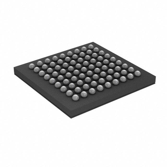


 工商网监
湘ICP备2023018690号
工商网监
湘ICP备2023018690号
