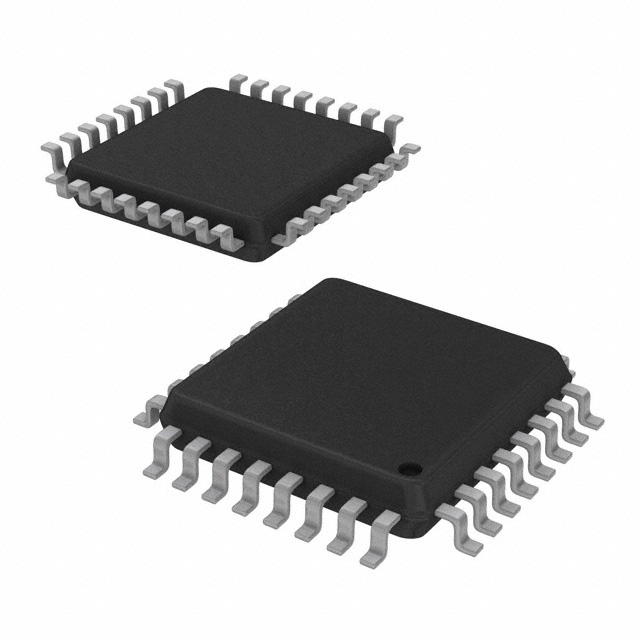
STM32L021D4 STM32L021F4
STM32L021G4 STM32L021K4
Access line ultra-low-power 32-bit MCU Arm®-based
Cortex®-M0+, 16KB Flash, 2KB SRAM, 512B EEPROM, ADC, AES
Datasheet - production data
Features
•
•
•
•
•
•
•
•
Ultra-low-power platform
– 1.65 V to 3.6 V power supply
– -40 to 125 °C temperature range
– 0.23 µA Standby mode (2 wakeup pins)
– 0.29 µA Stop mode (16 wakeup lines)
– 0.54 µA Stop mode + RTC + 2 KB RAM
retention
– Down to 76 µA/MHz in Run mode
– 5 µs wakeup time (from Flash memory)
– 41 µA 12-bit ADC conversion at 10 ksps
Core: Arm® 32-bit Cortex®-M0+
– From 32 kHz to 32 MHz max.
– 0.95 DMIPS/MHz
Reset and supply management
– Ultra-safe, low-power BOR (brownout reset)
with 5 selectable thresholds
– Ultralow power POR/PDR
– Programmable voltage detector (PVD)
Clock sources
– 0 to 32 MHz external clock
– 32 kHz oscillator for RTC with calibration
– High speed internal 16 MHz factory-trimmed RC
(+/- 1%)
– Internal low-power 37 kHz RC
– Internal multispeed low-power 65 kHz to
4.2 MHz RC
– PLL for CPU clock
Pre-programmed bootloader
– USART, SPI supported
Development support
– Serial wire debug supported
Up to 28 fast I/Os (23 I/Os 5V tolerant)
TSSOP14/20
169 mils
•
•
UFQFPN20 3x3 mm
UFQFPN28 4x4 mm
UFQFPN32 5x5 mm
LQFP32
7x7 mm
Rich Analog peripherals
– 12-bit ADC 1.14 Msps up to 10 channels (down
to 1.65 V)
– 2x ultra-low-power comparators (window mode
and wake up capability, down to 1.65 V)
5-channel DMA controller, supporting ADC, SPI,
I2C, USART, Timers, AES
•
4x peripherals communication interface
•
1x USART (ISO 7816, IrDA), 1x UART (low power)
•
1x SPI 16 Mbits/s
•
1x I2C (SMBus/PMBus)
•
7x timers: 1x 16-bit with up to 4 channels, 1x 16-bit
with up to 2 channels, 1x 16-bit ultra-low-power
timer, 1x SysTick, 1x RTC and 2x watchdogs
(independent/window)
•
CRC calculation unit, 96-bit unique ID
• Hardware Encryption Engine AES 128-bit
•
All packages are ECOPACK®2
Memories
– 16 KB Flash memory with ECC
– 2 KB RAM
– 512 B of data EEPROM with ECC
– 20-byte backup register
– Sector protection against R/W operation
–
September 2017
This is information on a product in full production.
DocID027982 Rev 5
1/114
www.st.com
�Contents
STM32L021x4
Contents
1
Introduction . . . . . . . . . . . . . . . . . . . . . . . . . . . . . . . . . . . . . . . . . . . . . . . . 9
2
Description . . . . . . . . . . . . . . . . . . . . . . . . . . . . . . . . . . . . . . . . . . . . . . . . 10
3
2.1
Device overview . . . . . . . . . . . . . . . . . . . . . . . . . . . . . . . . . . . . . . . . . . . . .11
2.2
Ultra-low-power device continuum . . . . . . . . . . . . . . . . . . . . . . . . . . . . . . 13
Functional overview . . . . . . . . . . . . . . . . . . . . . . . . . . . . . . . . . . . . . . . . 14
3.1
Low-power modes . . . . . . . . . . . . . . . . . . . . . . . . . . . . . . . . . . . . . . . . . . 14
3.2
Interconnect matrix . . . . . . . . . . . . . . . . . . . . . . . . . . . . . . . . . . . . . . . . . . 18
3.3
Arm® Cortex®-M0+ core . . . . . . . . . . . . . . . . . . . . . . . . . . . . . . . . . . . . . 19
3.4
Reset and supply management . . . . . . . . . . . . . . . . . . . . . . . . . . . . . . . . 20
3.4.1
Power supply schemes . . . . . . . . . . . . . . . . . . . . . . . . . . . . . . . . . . . . . 20
3.4.2
Power supply supervisor . . . . . . . . . . . . . . . . . . . . . . . . . . . . . . . . . . . . 20
3.4.3
Voltage regulator . . . . . . . . . . . . . . . . . . . . . . . . . . . . . . . . . . . . . . . . . . 21
3.4.4
Boot modes . . . . . . . . . . . . . . . . . . . . . . . . . . . . . . . . . . . . . . . . . . . . . . 21
3.5
Clock management . . . . . . . . . . . . . . . . . . . . . . . . . . . . . . . . . . . . . . . . . 22
3.6
Low-power real-time clock and backup registers . . . . . . . . . . . . . . . . . . . 24
3.7
General-purpose inputs/outputs (GPIOs) . . . . . . . . . . . . . . . . . . . . . . . . . 24
3.8
Memories . . . . . . . . . . . . . . . . . . . . . . . . . . . . . . . . . . . . . . . . . . . . . . . . . 25
3.9
Direct memory access (DMA) . . . . . . . . . . . . . . . . . . . . . . . . . . . . . . . . . 25
3.10
Analog-to-digital converter (ADC) . . . . . . . . . . . . . . . . . . . . . . . . . . . . . . 26
3.11
Temperature sensor . . . . . . . . . . . . . . . . . . . . . . . . . . . . . . . . . . . . . . . . . 26
3.11.1
2/114
Internal voltage reference (VREFINT) . . . . . . . . . . . . . . . . . . . . . . . . . . . 26
3.12
Ultra-low-power comparators and reference voltage . . . . . . . . . . . . . . . . 27
3.13
System configuration controller . . . . . . . . . . . . . . . . . . . . . . . . . . . . . . . . 27
3.14
AES . . . . . . . . . . . . . . . . . . . . . . . . . . . . . . . . . . . . . . . . . . . . . . . . . . . . . 27
3.15
Timers and watchdogs . . . . . . . . . . . . . . . . . . . . . . . . . . . . . . . . . . . . . . . 28
3.15.1
General-purpose timers (TIM2, TIM21) . . . . . . . . . . . . . . . . . . . . . . . . . 28
3.15.2
Low-power Timer (LPTIM) . . . . . . . . . . . . . . . . . . . . . . . . . . . . . . . . . . . 29
3.15.3
SysTick timer . . . . . . . . . . . . . . . . . . . . . . . . . . . . . . . . . . . . . . . . . . . . . 29
3.15.4
Independent watchdog (IWDG) . . . . . . . . . . . . . . . . . . . . . . . . . . . . . . . 29
3.15.5
Window watchdog (WWDG) . . . . . . . . . . . . . . . . . . . . . . . . . . . . . . . . . 29
DocID027982 Rev 5
�STM32L021x4
3.16
Contents
Communication interfaces . . . . . . . . . . . . . . . . . . . . . . . . . . . . . . . . . . . . 30
3.16.1
I2C bus . . . . . . . . . . . . . . . . . . . . . . . . . . . . . . . . . . . . . . . . . . . . . . . . . 30
3.16.2
Universal synchronous/asynchronous receiver transmitter (USART) . . 31
3.16.3
Low-power universal asynchronous receiver transmitter (LPUART) . . . 31
3.16.4
Serial peripheral interface (SPI) . . . . . . . . . . . . . . . . . . . . . . . . . . . . . . . 32
3.17
Cyclic redundancy check (CRC) calculation unit . . . . . . . . . . . . . . . . . . . 32
3.18
Serial wire debug port (SW-DP) . . . . . . . . . . . . . . . . . . . . . . . . . . . . . . . . 32
4
Pin descriptions . . . . . . . . . . . . . . . . . . . . . . . . . . . . . . . . . . . . . . . . . . . 33
5
Memory mapping . . . . . . . . . . . . . . . . . . . . . . . . . . . . . . . . . . . . . . . . . . . 43
6
Electrical characteristics . . . . . . . . . . . . . . . . . . . . . . . . . . . . . . . . . . . . 44
6.1
Parameter conditions . . . . . . . . . . . . . . . . . . . . . . . . . . . . . . . . . . . . . . . . 44
6.1.1
Minimum and maximum values . . . . . . . . . . . . . . . . . . . . . . . . . . . . . . . 44
6.1.2
Typical values . . . . . . . . . . . . . . . . . . . . . . . . . . . . . . . . . . . . . . . . . . . . 44
6.1.3
Typical curves . . . . . . . . . . . . . . . . . . . . . . . . . . . . . . . . . . . . . . . . . . . . 44
6.1.4
Loading capacitor . . . . . . . . . . . . . . . . . . . . . . . . . . . . . . . . . . . . . . . . . 44
6.1.5
Pin input voltage . . . . . . . . . . . . . . . . . . . . . . . . . . . . . . . . . . . . . . . . . . 44
6.1.6
Power supply scheme . . . . . . . . . . . . . . . . . . . . . . . . . . . . . . . . . . . . . . 45
6.1.7
Current consumption measurement . . . . . . . . . . . . . . . . . . . . . . . . . . . 45
6.2
Absolute maximum ratings . . . . . . . . . . . . . . . . . . . . . . . . . . . . . . . . . . . . 46
6.3
Operating conditions . . . . . . . . . . . . . . . . . . . . . . . . . . . . . . . . . . . . . . . . 48
6.3.1
General operating conditions . . . . . . . . . . . . . . . . . . . . . . . . . . . . . . . . . 48
6.3.2
Embedded reset and power control block characteristics . . . . . . . . . . . 49
6.3.3
Embedded internal reference voltage . . . . . . . . . . . . . . . . . . . . . . . . . . 51
6.3.4
Supply current characteristics . . . . . . . . . . . . . . . . . . . . . . . . . . . . . . . . 52
6.3.5
Wakeup time from low-power mode . . . . . . . . . . . . . . . . . . . . . . . . . . . 62
6.3.6
External clock source characteristics . . . . . . . . . . . . . . . . . . . . . . . . . . . 64
6.3.7
Internal clock source characteristics . . . . . . . . . . . . . . . . . . . . . . . . . . . 67
6.3.8
PLL characteristics . . . . . . . . . . . . . . . . . . . . . . . . . . . . . . . . . . . . . . . . 69
6.3.9
Memory characteristics . . . . . . . . . . . . . . . . . . . . . . . . . . . . . . . . . . . . . 70
6.3.10
EMC characteristics . . . . . . . . . . . . . . . . . . . . . . . . . . . . . . . . . . . . . . . . 72
6.3.11
Electrical sensitivity characteristics . . . . . . . . . . . . . . . . . . . . . . . . . . . . 73
6.3.12
I/O current injection characteristics . . . . . . . . . . . . . . . . . . . . . . . . . . . . 74
6.3.13
I/O port characteristics . . . . . . . . . . . . . . . . . . . . . . . . . . . . . . . . . . . . . . 75
6.3.14
NRST pin characteristics . . . . . . . . . . . . . . . . . . . . . . . . . . . . . . . . . . . . 79
DocID027982 Rev 5
3/114
4
�Contents
7
STM32L021x4
6.3.15
12-bit ADC characteristics . . . . . . . . . . . . . . . . . . . . . . . . . . . . . . . . . . . 80
6.3.16
Temperature sensor characteristics . . . . . . . . . . . . . . . . . . . . . . . . . . . . 84
6.3.17
Comparators . . . . . . . . . . . . . . . . . . . . . . . . . . . . . . . . . . . . . . . . . . . . . 85
6.3.18
Timer characteristics . . . . . . . . . . . . . . . . . . . . . . . . . . . . . . . . . . . . . . . 86
6.3.19
Communications interfaces . . . . . . . . . . . . . . . . . . . . . . . . . . . . . . . . . . 87
Package information . . . . . . . . . . . . . . . . . . . . . . . . . . . . . . . . . . . . . . . . 94
7.1
LQFP32 package information . . . . . . . . . . . . . . . . . . . . . . . . . . . . . . . . . . 94
7.2
UFQFPN32 package information . . . . . . . . . . . . . . . . . . . . . . . . . . . . . . . 97
7.3
UFQFPN28 4 x 4 mm package information . . . . . . . . . . . . . . . . . . . . . . . 99
7.4
UFQFPN20 package information . . . . . . . . . . . . . . . . . . . . . . . . . . . . . . 102
7.5
TSSOP20 package information . . . . . . . . . . . . . . . . . . . . . . . . . . . . . . . 105
7.6
TSSOP14 package information . . . . . . . . . . . . . . . . . . . . . . . . . . . . . . . 107
7.7
Thermal characteristics . . . . . . . . . . . . . . . . . . . . . . . . . . . . . . . . . . . . . 108
7.7.1
Reference document . . . . . . . . . . . . . . . . . . . . . . . . . . . . . . . . . . . . . . 109
8
Ordering information . . . . . . . . . . . . . . . . . . . . . . . . . . . . . . . . . . . . . . 110
9
Revision history . . . . . . . . . . . . . . . . . . . . . . . . . . . . . . . . . . . . . . . . . . 111
4/114
DocID027982 Rev 5
�STM32L021x4
List of tables
List of tables
Table 1.
Table 2.
Table 3.
Table 4.
Table 5.
Table 6.
Table 7.
Table 8.
Table 9.
Table 10.
Table 11.
Table 12.
Table 13.
Table 14.
Table 15.
Table 16.
Table 17.
Table 18.
Table 19.
Table 20.
Table 21.
Table 22.
Table 23.
Table 24.
Table 25.
Table 26.
Table 27.
Table 28.
Table 29.
Table 30.
Table 31.
Table 32.
Table 33.
Table 34.
Table 35.
Table 36.
Table 37.
Table 38.
Table 39.
Table 40.
Table 41.
Table 42.
Table 43.
Table 44.
Table 45.
Ultra-low-power STM32L021x4 device features and peripheral counts . . . . . . . . . . . . . . . 11
Functionalities depending on the operating power supply range . . . . . . . . . . . . . . . . . . . . 16
CPU frequency range depending on dynamic voltage scaling . . . . . . . . . . . . . . . . . . . . . . 16
Functionalities depending on the working mode
(from Run/active down to standby) . . . . . . . . . . . . . . . . . . . . . . . . . . . . . . . . . . . . . . . . . . 17
STM32L021x4 peripherals interconnect matrix . . . . . . . . . . . . . . . . . . . . . . . . . . . . . . . . . 19
Timer feature comparison . . . . . . . . . . . . . . . . . . . . . . . . . . . . . . . . . . . . . . . . . . . . . . . . . . 28
Comparison of I2C analog and digital filters . . . . . . . . . . . . . . . . . . . . . . . . . . . . . . . . . . . . 30
STM32L021x4 I2C implementation . . . . . . . . . . . . . . . . . . . . . . . . . . . . . . . . . . . . . . . . . . . 30
USART implementation . . . . . . . . . . . . . . . . . . . . . . . . . . . . . . . . . . . . . . . . . . . . . . . . . . . 31
SPI implementation. . . . . . . . . . . . . . . . . . . . . . . . . . . . . . . . . . . . . . . . . . . . . . . . . . . . . . . 32
Legend/abbreviations used in the pinout table . . . . . . . . . . . . . . . . . . . . . . . . . . . . . . . . . . 35
Pin definitions . . . . . . . . . . . . . . . . . . . . . . . . . . . . . . . . . . . . . . . . . . . . . . . . . . . . . . . . . . . 36
Alternate functions . . . . . . . . . . . . . . . . . . . . . . . . . . . . . . . . . . . . . . . . . . . . . . . . . . . . . . . 41
Voltage characteristics . . . . . . . . . . . . . . . . . . . . . . . . . . . . . . . . . . . . . . . . . . . . . . . . . . . . 46
Current characteristics . . . . . . . . . . . . . . . . . . . . . . . . . . . . . . . . . . . . . . . . . . . . . . . . . . . . 47
Thermal characteristics. . . . . . . . . . . . . . . . . . . . . . . . . . . . . . . . . . . . . . . . . . . . . . . . . . . . 47
General operating conditions . . . . . . . . . . . . . . . . . . . . . . . . . . . . . . . . . . . . . . . . . . . . . . . 48
Embedded reset and power control block characteristics. . . . . . . . . . . . . . . . . . . . . . . . . . 49
Embedded internal reference voltage calibration values . . . . . . . . . . . . . . . . . . . . . . . . . . 51
Embedded internal reference voltage . . . . . . . . . . . . . . . . . . . . . . . . . . . . . . . . . . . . . . . . . 51
Current consumption in Run mode, code with data processing running from Flash. . . . . . 53
Current consumption in Run mode vs code type,
code with data processing running from Flash . . . . . . . . . . . . . . . . . . . . . . . . . . . . . . . . . . 53
Current consumption in Run mode, code with data processing running from RAM . . . . . . 55
Current consumption in Run mode vs code type,
code with data processing running from RAM . . . . . . . . . . . . . . . . . . . . . . . . . . . . . . . . . . 55
Current consumption in Sleep mode . . . . . . . . . . . . . . . . . . . . . . . . . . . . . . . . . . . . . . . . . 56
Current consumption in Low-power Run mode . . . . . . . . . . . . . . . . . . . . . . . . . . . . . . . . . 57
Current consumption in Low-power Sleep mode . . . . . . . . . . . . . . . . . . . . . . . . . . . . . . . . 58
Typical and maximum current consumptions in Stop mode . . . . . . . . . . . . . . . . . . . . . . . . 59
Typical and maximum current consumptions in Standby mode . . . . . . . . . . . . . . . . . . . . . 60
Average current consumption during wakeup . . . . . . . . . . . . . . . . . . . . . . . . . . . . . . . . . . 60
Peripheral current consumption in run or Sleep mode . . . . . . . . . . . . . . . . . . . . . . . . . . . . 61
Peripheral current consumption in Stop and Standby mode . . . . . . . . . . . . . . . . . . . . . . . 62
Low-power mode wakeup timings . . . . . . . . . . . . . . . . . . . . . . . . . . . . . . . . . . . . . . . . . . . 62
High-speed external user clock characteristics. . . . . . . . . . . . . . . . . . . . . . . . . . . . . . . . . . 64
Low-speed external user clock characteristics . . . . . . . . . . . . . . . . . . . . . . . . . . . . . . . . . . 65
LSE oscillator characteristics . . . . . . . . . . . . . . . . . . . . . . . . . . . . . . . . . . . . . . . . . . . . . . . 66
16 MHz HSI16 oscillator characteristics . . . . . . . . . . . . . . . . . . . . . . . . . . . . . . . . . . . . . . . 67
LSI oscillator characteristics . . . . . . . . . . . . . . . . . . . . . . . . . . . . . . . . . . . . . . . . . . . . . . . . 68
MSI oscillator characteristics . . . . . . . . . . . . . . . . . . . . . . . . . . . . . . . . . . . . . . . . . . . . . . . 68
PLL characteristics . . . . . . . . . . . . . . . . . . . . . . . . . . . . . . . . . . . . . . . . . . . . . . . . . . . . . . . 69
RAM and hardware registers . . . . . . . . . . . . . . . . . . . . . . . . . . . . . . . . . . . . . . . . . . . . . . . 70
Flash memory and data EEPROM characteristics . . . . . . . . . . . . . . . . . . . . . . . . . . . . . . . 71
Flash memory and data EEPROM endurance and retention . . . . . . . . . . . . . . . . . . . . . . . 71
EMS characteristics . . . . . . . . . . . . . . . . . . . . . . . . . . . . . . . . . . . . . . . . . . . . . . . . . . . . . . 72
EMI characteristics . . . . . . . . . . . . . . . . . . . . . . . . . . . . . . . . . . . . . . . . . . . . . . . . . . . . . . . 73
DocID027982 Rev 5
5/114
6
�List of tables
Table 46.
Table 47.
Table 48.
Table 49.
Table 50.
Table 51.
Table 52.
Table 53.
Table 54.
Table 55.
Table 56.
Table 57.
Table 58.
Table 59.
Table 60.
Table 61.
Table 62.
Table 63.
Table 64.
Table 65.
Table 66.
Table 67.
Table 68.
Table 69.
Table 70.
Table 71.
Table 72.
Table 73.
Table 74.
Table 75.
6/114
STM32L021x4
ESD absolute maximum ratings . . . . . . . . . . . . . . . . . . . . . . . . . . . . . . . . . . . . . . . . . . . . . 73
Electrical sensitivities . . . . . . . . . . . . . . . . . . . . . . . . . . . . . . . . . . . . . . . . . . . . . . . . . . . . . 74
I/O current injection susceptibility . . . . . . . . . . . . . . . . . . . . . . . . . . . . . . . . . . . . . . . . . . . . 74
I/O static characteristics . . . . . . . . . . . . . . . . . . . . . . . . . . . . . . . . . . . . . . . . . . . . . . . . . . . 75
Output voltage characteristics . . . . . . . . . . . . . . . . . . . . . . . . . . . . . . . . . . . . . . . . . . . . . . 77
I/O AC characteristics . . . . . . . . . . . . . . . . . . . . . . . . . . . . . . . . . . . . . . . . . . . . . . . . . . . . . 78
NRST pin characteristics . . . . . . . . . . . . . . . . . . . . . . . . . . . . . . . . . . . . . . . . . . . . . . . . . . 79
ADC characteristics . . . . . . . . . . . . . . . . . . . . . . . . . . . . . . . . . . . . . . . . . . . . . . . . . . . . . . 80
RAIN max for fADC = 16 MHz . . . . . . . . . . . . . . . . . . . . . . . . . . . . . . . . . . . . . . . . . . . . . . . . 82
ADC accuracy . . . . . . . . . . . . . . . . . . . . . . . . . . . . . . . . . . . . . . . . . . . . . . . . . . . . . . . . . . . 82
Temperature sensor calibration values. . . . . . . . . . . . . . . . . . . . . . . . . . . . . . . . . . . . . . . . 84
Temperature sensor characteristics . . . . . . . . . . . . . . . . . . . . . . . . . . . . . . . . . . . . . . . . . . 84
Comparator 1 characteristics . . . . . . . . . . . . . . . . . . . . . . . . . . . . . . . . . . . . . . . . . . . . . . . 85
Comparator 2 characteristics . . . . . . . . . . . . . . . . . . . . . . . . . . . . . . . . . . . . . . . . . . . . . . . 85
TIMx characteristics . . . . . . . . . . . . . . . . . . . . . . . . . . . . . . . . . . . . . . . . . . . . . . . . . . . . . . 86
I2C analog filter characteristics. . . . . . . . . . . . . . . . . . . . . . . . . . . . . . . . . . . . . . . . . . . . . . 87
I2C frequency in all I2C modes. . . . . . . . . . . . . . . . . . . . . . . . . . . . . . . . . . . . . . . . . . . . . . 88
SPI characteristics in voltage Range 1 . . . . . . . . . . . . . . . . . . . . . . . . . . . . . . . . . . . . . . . 89
SPI characteristics in voltage Range 2 . . . . . . . . . . . . . . . . . . . . . . . . . . . . . . . . . . . . . . . 90
SPI characteristics in voltage Range 3 . . . . . . . . . . . . . . . . . . . . . . . . . . . . . . . . . . . . . . . 91
LQFP32 - 32-pin, 7 x 7 mm, 32-pin low-profile quad flat package
mechanical data . . . . . . . . . . . . . . . . . . . . . . . . . . . . . . . . . . . . . . . . . . . . . . . . . . . . . . . . . 95
UFQFPN32 - 32-pin, 5x5 mm, 0.5 mm pitch ultra thin fine pitch quad flat
package mechanical data . . . . . . . . . . . . . . . . . . . . . . . . . . . . . . . . . . . . . . . . . . . . . . . . . . 98
WLCSP25 - 25-ball, 2.133 x 2.070 mm, 0.4 mm pitch wafer level chip scale
package mechanical data . . . . . . . . . . . . . . . . . . . . . . . . . . . . . . . . . . . . . . . . . . . . . . . . . . 99
UFQFPN28 - 28-lead, 4x4 mm, 0.5 mm pitch, ultra thin fine pitch quad flat
package mechanical data . . . . . . . . . . . . . . . . . . . . . . . . . . . . . . . . . . . . . . . . . . . . . . . . . 100
UFQFPN20 - 20-lead, 3x3 mm, 0.5 mm pitch, ultra thin fine pitch quad flat
package mechanical data . . . . . . . . . . . . . . . . . . . . . . . . . . . . . . . . . . . . . . . . . . . . . . . . . 102
TSSOP20 – 20-lead thin shrink small outline, 6.5 x 4.4 mm, 0.65 mm pitch,
package mechanical data . . . . . . . . . . . . . . . . . . . . . . . . . . . . . . . . . . . . . . . . . . . . . . . . . 105
TSSOP14 – 14-lead thin shrink small outline, 5 x 4.4 mm, 0.65 mm pitch,
package mechanical data . . . . . . . . . . . . . . . . . . . . . . . . . . . . . . . . . . . . . . . . . . . . . . . . . 107
Thermal characteristics. . . . . . . . . . . . . . . . . . . . . . . . . . . . . . . . . . . . . . . . . . . . . . . . . . . 109
STM32L021x4 ordering information scheme . . . . . . . . . . . . . . . . . . . . . . . . . . . . . . . . . . 110
Document revision history . . . . . . . . . . . . . . . . . . . . . . . . . . . . . . . . . . . . . . . . . . . . . . . . 111
DocID027982 Rev 5
�STM32L021x4
List of figures
List of figures
Figure 1.
Figure 2.
Figure 3.
Figure 4.
Figure 5.
Figure 6.
Figure 7.
Figure 8.
Figure 9.
Figure 10.
Figure 11.
Figure 12.
Figure 13.
Figure 14.
Figure 15.
Figure 16.
Figure 17.
Figure 18.
Figure 19.
Figure 20.
Figure 21.
Figure 22.
Figure 23.
Figure 24.
Figure 25.
Figure 26.
Figure 27.
Figure 28.
Figure 29.
Figure 30.
Figure 31.
Figure 32.
Figure 33.
Figure 34.
Figure 35.
Figure 36.
Figure 37.
Figure 38.
Figure 39.
Figure 40.
STM32L021x4 block diagram . . . . . . . . . . . . . . . . . . . . . . . . . . . . . . . . . . . . . . . . . . . . . . . 12
Clock tree . . . . . . . . . . . . . . . . . . . . . . . . . . . . . . . . . . . . . . . . . . . . . . . . . . . . . . . . . . . . . 23
STM32L021x4 LQFP32 pinout . . . . . . . . . . . . . . . . . . . . . . . . . . . . . . . . . . . . . . . . . . . . . 33
STM32L021x4 UFQFPN32 pinout . . . . . . . . . . . . . . . . . . . . . . . . . . . . . . . . . . . . . . . . . . . 33
STM32L021x4 UFQFPN28 pinout . . . . . . . . . . . . . . . . . . . . . . . . . . . . . . . . . . . . . . . . . . . 34
STM32L021x4 UFQFPN20 pinout . . . . . . . . . . . . . . . . . . . . . . . . . . . . . . . . . . . . . . . . . . . 34
STM32L021x4 TSSOP20 pinout . . . . . . . . . . . . . . . . . . . . . . . . . . . . . . . . . . . . . . . . . . . . 35
STM32L021x4 TSSOP14 pinout . . . . . . . . . . . . . . . . . . . . . . . . . . . . . . . . . . . . . . . . . . . . 35
Pin loading conditions . . . . . . . . . . . . . . . . . . . . . . . . . . . . . . . . . . . . . . . . . . . . . . . . . . . . . 44
Pin input voltage . . . . . . . . . . . . . . . . . . . . . . . . . . . . . . . . . . . . . . . . . . . . . . . . . . . . . . . . . 44
Power supply scheme. . . . . . . . . . . . . . . . . . . . . . . . . . . . . . . . . . . . . . . . . . . . . . . . . . . . . 45
Current consumption measurement scheme . . . . . . . . . . . . . . . . . . . . . . . . . . . . . . . . . . . 45
IDD vs VDD, at TA= 25 °C, Run mode, code running from
Flash memory, Range 2, 16 MHz HSE, 1WS . . . . . . . . . . . . . . . . . . . . . . . . . . . . . . . . . . . 54
IDD vs VDD, at TA= 25 °C, Run mode, code running from
Flash memory, Range 2, HSI16, 1WS . . . . . . . . . . . . . . . . . . . . . . . . . . . . . . . . . . . . . . . . 54
IDD vs VDD, at TA= -40/25/55/ 85/105/125 °C, Low-power run mode,
code running from RAM, Range 3, MSI (Range 0) at 64 KHz, 0 WS . . . . . . . . . . . . . . . . . 58
IDD vs VDD, at TA= -40/25/55/ 85/105/125 °C, Stop mode with RTC enabled
and running on LSE Low drive . . . . . . . . . . . . . . . . . . . . . . . . . . . . . . . . . . . . . . . . . . . . . . 59
IDD vs VDD, at TA= -40/25/55/85/105/125 °C, Stop mode with RTC disabled,
all clocks OFF . . . . . . . . . . . . . . . . . . . . . . . . . . . . . . . . . . . . . . . . . . . . . . . . . . . . . . . . . . . 59
High-speed external clock source AC timing diagram . . . . . . . . . . . . . . . . . . . . . . . . . . . . 64
Low-speed external clock source AC timing diagram . . . . . . . . . . . . . . . . . . . . . . . . . . . . . 65
Typical application with a 32.768 kHz crystal . . . . . . . . . . . . . . . . . . . . . . . . . . . . . . . . . . . 66
HSI16 minimum and maximum value versus temperature . . . . . . . . . . . . . . . . . . . . . . . . . 67
VIH/VIL versus VDD (CMOS I/Os) . . . . . . . . . . . . . . . . . . . . . . . . . . . . . . . . . . . . . . . . . . . 76
VIH/VIL versus VDD (TTL I/Os) . . . . . . . . . . . . . . . . . . . . . . . . . . . . . . . . . . . . . . . . . . . . . 76
I/O AC characteristics definition . . . . . . . . . . . . . . . . . . . . . . . . . . . . . . . . . . . . . . . . . . . . . 79
Recommended NRST pin protection . . . . . . . . . . . . . . . . . . . . . . . . . . . . . . . . . . . . . . . . . 80
ADC accuracy characteristics . . . . . . . . . . . . . . . . . . . . . . . . . . . . . . . . . . . . . . . . . . . . . . . 83
Typical connection diagram using the ADC . . . . . . . . . . . . . . . . . . . . . . . . . . . . . . . . . . . . 84
SPI timing diagram - slave mode and CPHA = 0 . . . . . . . . . . . . . . . . . . . . . . . . . . . . . . . . 92
SPI timing diagram - slave mode and CPHA = 1(1) . . . . . . . . . . . . . . . . . . . . . . . . . . . . . . 92
SPI timing diagram - master mode(1) . . . . . . . . . . . . . . . . . . . . . . . . . . . . . . . . . . . . . . . . . 93
LQFP32 - 32-pin, 7 x 7 mm, 32-pin low-profile quad flat package outline . . . . . . . . . . . . . 94
LQFP32 recommended footprint . . . . . . . . . . . . . . . . . . . . . . . . . . . . . . . . . . . . . . . . . . . . 95
Example of LQFP32 marking (package top view) . . . . . . . . . . . . . . . . . . . . . . . . . . . . . . . 96
UFQFPN32 - 32-pin, 5x5 mm, 0.5 mm pitch ultra thin fine pitch quad flat
package outline. . . . . . . . . . . . . . . . . . . . . . . . . . . . . . . . . . . . . . . . . . . . . . . . . . . . . . . . . . 97
UFQFPN32 recommended footprint . . . . . . . . . . . . . . . . . . . . . . . . . . . . . . . . . . . . . . . . . . 98
UFQFPN28 - 28-lead, 4x4 mm, 0.5 mm pitch, ultra thin fine pitch quad flat
package outline. . . . . . . . . . . . . . . . . . . . . . . . . . . . . . . . . . . . . . . . . . . . . . . . . . . . . . . . . . 99
UFQFPN28 recommended footprint . . . . . . . . . . . . . . . . . . . . . . . . . . . . . . . . . . . . . . . . . 101
Example of UFQFPN28 marking (package top view) . . . . . . . . . . . . . . . . . . . . . . . . . . . . 101
UFQFPN20 - 20-lead, 3x3 mm, 0.5 mm pitch, ultra thin fine pitch quad flat
package outline. . . . . . . . . . . . . . . . . . . . . . . . . . . . . . . . . . . . . . . . . . . . . . . . . . . . . . . . . 102
UFQFPN20 - 20-lead, 3x3 mm, 0.5 mm pitch, ultra thin fine pitch quad flat
DocID027982 Rev 5
7/114
8
�List of figures
Figure 41.
Figure 42.
Figure 43.
Figure 44.
Figure 45.
Figure 46.
8/114
STM32L021x4
package recommended footprint . . . . . . . . . . . . . . . . . . . . . . . . . . . . . . . . . . . . . . . . . . . 103
Example of UFQFPN20 marking (package top view) . . . . . . . . . . . . . . . . . . . . . . . . . . . . 104
TSSOP20 – 20-lead thin shrink small outline, 6.5 x 4.4 mm, 0.65 mm pitch,
package outline. . . . . . . . . . . . . . . . . . . . . . . . . . . . . . . . . . . . . . . . . . . . . . . . . . . . . . . . . 105
TSSOP20 – 20-lead thin shrink small outline, 6.5 x 4.4 mm, 0.65 mm pitch,
package footprint . . . . . . . . . . . . . . . . . . . . . . . . . . . . . . . . . . . . . . . . . . . . . . . . . . . . . . . 106
TSSOP14 – 14-lead thin shrink small outline, 5.0 x 4.4 mm, 0.65 mm pitch,
package outline. . . . . . . . . . . . . . . . . . . . . . . . . . . . . . . . . . . . . . . . . . . . . . . . . . . . . . . . . 107
Example of TSSOP14 marking (package top view) . . . . . . . . . . . . . . . . . . . . . . . . . . . . . 108
Thermal resistance . . . . . . . . . . . . . . . . . . . . . . . . . . . . . . . . . . . . . . . . . . . . . . . . . . . . . . 109
DocID027982 Rev 5
�STM32L021x4
1
Introduction
Introduction
The ultra-low-power STM32L021x4 family includes devices in 6 different package types
from 14 to 32 pins. The description below gives an overview of the complete range of
peripherals proposed in this family.
These features make the ultra-low-power STM32L021x4 microcontrollers suitable for a wide
range of applications:
•
Gas/water meters and industrial sensors
•
Healthcare and fitness equipment
•
Remote control and user interface
•
PC peripherals, gaming, GPS equipment
•
Alarm system, wired and wireless sensors, video intercom
This STM32L021x4 datasheet should be read in conjunction with the STM32L0x1 reference
manual (RM0377).
For information on the Arm® Cortex®-M0+ core please refer to the Cortex®-M0+ Technical
Reference Manual, available from the www.arm.com website.
Figure 1 shows the general block diagram of the device family.
DocID027982 Rev 5
9/114
32
�Description
2
STM32L021x4
Description
The access line ultra-low-power STM32L021x4 family incorporates the high-performance
Arm® Cortex®-M0+ 32-bit RISC core operating at a 32 MHz frequency, high-speed
embedded memories (16 Kbytes of Flash program memory, 512 bytes of data EEPROM and
2 Kbytes of RAM) plus an extensive range of enhanced I/Os and peripherals.
The STM32L021x4 devices provide high power efficiency for a wide range of performance.
It is achieved with a large choice of internal and external clock sources, an internal voltage
adaptation and several low-power modes.
The STM32L021x4 devices offer several analog features, one 12-bit ADC with hardware
oversampling, two ultra-low-power comparators, AES, several timers, one low-power timer
(LPTIM), three general-purpose 16-bit timers, one RTC and one SysTick which can be used
as timebases. They also feature two watchdogs, one watchdog with independent clock and
window capability and one window watchdog based on bus clock.
Moreover, the STM32L021x4 devices embed standard and advanced communication
interfaces: one I2C, one SPI, one USART, and a low-power UART (LPUART).
The STM32L021x4 also include a real-time clock and a set of backup registers that remain
powered in Standby mode.
The ultra-low-power STM32L021x4 devices operate from a 1.8 to 3.6 V power supply (down
to 1.65 V at power down) with BOR and from a 1.65 to 3.6 V power supply without BOR
option. They are available in the -40 to +125 °C temperature range. A comprehensive set of
power-saving modes allows the design of low-power applications.
10/114
DocID027982 Rev 5
�STM32L021x4
2.1
Description
Device overview
Table 1. Ultra-low-power STM32L021x4 device features and peripheral counts
Peripheral
STM32 L021D4 STM32 L021F4 STM32 L021G4 STM32L021K4
Flash (Kbytes)
16
Data EEPROM (bytes)
512
RAM (Kbytes)
2
AES
1
Timers
Generalpurpose
2
LPTIM
1
RTC/SYSTICK/IWDG/
WWDG
Communication
interfaces
1/1/1/1
SPI
1
I2C
1
USART
1
LPUART
1
GPIOs
11
16
Clocks: HSE(2)/LSE/HSI/MSI/LSI
12-bit synchronized ADC
Number of channels
1/1/1/1/1
1
4
1
10
1
7/9(3)
Comparators
2
Max. CPU frequency
Operating voltage
32 MHz
1.8 V to 3.6 V (down to 1.65 V at power-down) with BOR option
1.65 V to 3.6 V without BOR option
Ambient temperature: –40 to +125 °C
Junction temperature: –40 to +130 °C
Operating temperatures
Packages
26/28(1)
24
TSSOP14
TSSOP20,
UFQFPN20
UFQFPN28
LQFP32,
UFQFPN32
1. The devices feature 26 and 28 GPIOs on LQFP32 and UFQFPN32, respectively.
2. HSE available only as external clock input (HSE bypass).
3. The devices feature 7 and 9 ADC channels on UFQFPN20 and TSSOP20, respectively.
DocID027982 Rev 5
11/114
32
�Description
STM32L021x4
Figure 1. STM32L021x4 block diagram
7HPS�
VHQVRU
6:'
6:'
)/$6+
((3520
%227
&257(;�0���&38
)PD[���0+]
$'&�
$,1[
63,�
0,62��026,��
6&.��166
5$0
'%*
'0$�
19,&
(;7,
$
3
%
�
7,0��
�FK
%5,'*(
&203�
,13��,10��287
&203�
,13��,10��287
/37,0�
,1���,1���
(75��287
&5&
%5,'*(
*3,2�3257�$
3%>����@
*3,2�3257�%
3&>�����@
*3,2�3257�&
3+>���@
&.B,1
$+%��)PD[���0+]
3$>����@
$(6
::'*
$
3
%
�
*3,2�3257�+
+6(
,�&�
6&/��6'$��
60%$
86$57�
5;��7;��576�
&76��&.
/38$57�
5;��7;��576��
&76
+6,���0
/6,
,:'*
3//
06,
7,0�
�FK
57&
%&.3�5(*
5(6(7� �&/.
:.83[
26&��B,1�
26&��B287
/6(
39'B,1
95()B287
308
1567
9''$
9''
5(*8/$725
06Y�����9�
12/114
DocID027982 Rev 5
�STM32L021x4
2.2
Description
Ultra-low-power device continuum
The ultra-low-power family offers a large choice of core and features, from 8-bit proprietary
core up to Arm® Cortex®-M4, including Arm® Cortex®-M3 and Arm® Cortex®-M0+. The
STM32Lx series are the best choice to answer your needs in terms of ultra-low-power
features. The STM32 Ultra-low-power series are the best solution for applications such as
gas/water meter, keyboard/mouse or fitness and healthcare application. Several built-in
features like LCD drivers, dual-bank memory, low-power Run mode, operational amplifiers,
128-bit AES, DAC, crystal-less USB and many other definitely help you building a highly
cost optimized application by reducing BOM cost. STMicroelectronics, as a reliable and
long-term manufacturer, ensures as much as possible pin-to-pin compatibility between all
STM8Lx and STM32Lx on one hand, and between all STM32Lx and STM32Fx on the other
hand. Thanks to this unprecedented scalability, your legacy application can be upgraded to
respond to the latest market feature and efficiency requirements.
DocID027982 Rev 5
13/114
32
�Functional overview
STM32L021x4
3
Functional overview
3.1
Low-power modes
The ultra-low-power STM32L021x4 supports dynamic voltage scaling to optimize its power
consumption in Run mode. The voltage from the internal low-drop regulator that supplies
the logic can be adjusted according to the system’s maximum operating frequency and the
external voltage supply.
There are three power consumption ranges:
•
Range 1 (VDD range limited to 1.71-3.6 V), with the CPU running at up to 32 MHz
•
Range 2 (full VDD range), with a maximum CPU frequency of 16 MHz
•
Range 3 (full VDD range), with a maximum CPU frequency limited to 4.2 MHz
Seven low-power modes are provided to achieve the best compromise between low-power
consumption, short startup time and available wakeup sources:
•
Sleep mode
In Sleep mode, only the CPU is stopped. All peripherals continue to operate and can
wake up the CPU when an interrupt/event occurs. Sleep mode power consumption at
16 MHz is about 1 mA with all peripherals off.
•
Low-power run mode
This mode is achieved with the multispeed internal (MSI) RC oscillator set to the lowspeed clock (max 131 kHz), execution from SRAM or Flash memory, and internal
regulator in low-power mode to minimize the regulator's operating current. In Lowpower run mode, the clock frequency and the number of enabled peripherals are both
limited.
•
Low-power sleep mode
This mode is achieved by entering Sleep mode with the internal voltage regulator in
low-power mode to minimize the regulator’s operating current. In Low-power sleep
mode, both the clock frequency and the number of enabled peripherals are limited; a
typical example would be to have a timer running at 32 kHz.
When wakeup is triggered by an event or an interrupt, the system reverts to the Run
mode with the regulator on.
•
Stop mode with RTC
The Stop mode achieves the lowest power consumption while retaining the RAM and
register contents and real time clock. All clocks in the VCORE domain are stopped, the
PLL, MSI RC, HSE and HSI RC oscillators are disabled. The LSE or LSI is still running.
The voltage regulator is in the low-power mode.
Some peripherals featuring wakeup capability can enable the HSI RC during Stop
mode to detect their wakeup condition.
The device can be woken up from Stop mode by any of the EXTI line, in 3.5 µs, the
processor can serve the interrupt or resume the code. The EXTI line source can be any
GPIO. It can be the PVD output, the comparator 1 event or comparator 2 event
14/114
DocID027982 Rev 5
�STM32L021x4
Functional overview
(if internal reference voltage is on), it can be the RTC alarm/tamper/timestamp/wakeup
events, the USART/I2C/LPUART/LPTIM wakeup events.
•
Stop mode without RTC
The Stop mode achieves the lowest power consumption while retaining the RAM and
register contents. All clocks are stopped, the PLL, MSI RC, HSI and LSI RC, HSE and
LSE crystal oscillator are disabled.
Some peripherals featuring wakeup capability can enable the HSI RC during Stop
mode to detect their wakeup condition.
The voltage regulator is in the low-power mode. The device can be woken up from Stop
mode by any of the EXTI line, in 3.5 µs, the processor can serve the interrupt or
resume the code. The EXTI line source can be any GPIO. It can be the PVD output, the
comparator 1 event or comparator 2 event (if internal reference voltage is on). It can
also be wakened by the USART/I2C/LPUART/LPTIM wakeup events.
•
Standby mode with RTC
The Standby mode is used to achieve the lowest power consumption and real time
clock. The internal voltage regulator is switched off so that the entire VCORE domain is
powered off. The PLL, MSI RC, HSE bypass and HSI RC oscillators are also switched
off. The LSE or LSI is still running. After entering Standby mode, the RAM and register
contents are lost except for registers in the Standby circuitry (wakeup logic, IWDG,
RTC, LSI, LSE Crystal 32 KHz oscillator, RCC_CSR register).
The device exits Standby mode in 60 µs when an external reset (NRST pin), an IWDG
reset, a rising edge on one of the three WKUP pins, RTC alarm (Alarm A or Alarm B),
RTC tamper event, RTC timestamp event or RTC Wakeup event occurs.
•
Standby mode without RTC
The Standby mode is used to achieve the lowest power consumption. The internal
voltage regulator is switched off so that the entire VCORE domain is powered off. The
PLL, MSI RC, HSI and LSI RC, HSE and LSE crystal oscillator are also switched off.
After entering Standby mode, the RAM and register contents are lost except for
registers in the Standby circuitry (wakeup logic, IWDG, RTC, LSI, LSE Crystal 32 KHz
oscillator, RCC_CSR register).
The device exits Standby mode in 60 µs when an external reset (NRST pin) or a rising
edge on one of the three WKUP pin occurs.
Note:
The RTC, the IWDG, and the corresponding clock sources are not stopped automatically by
entering Stop or Standby mode.
DocID027982 Rev 5
15/114
32
�Functional overview
STM32L021x4
Table 2. Functionalities depending on the operating power supply range
Functionalities depending on the operating power
supply range
Operating power supply range
ADC operation
Dynamic voltage scaling
range
VDD = 1.65 to 1.71 V
ADC only, conversion time
up to 570 ksps
Range 2 or
range 3
VDD = 1.71 to 1.8 V(1)
ADC only, conversion time
up to 1.14 Msps
Range 1, range 2 or range 3
VDD = 1.8 to 2.0 V(1)
Conversion time up to 1.14
Msps
Range1, range 2 or range 3
VDD = 2.0 to 2.4 V
Conversion time up to 1.14
Msps
Range 1, range 2 or range 3
VDD = 2.4 to 3.6 V
Conversion time up to 1.14
Msps
Range 1, range 2 or range 3
1. CPU frequency changes from initial to final must respect the condition: fCPU initial